US9531361B2 - Power efficient multiplexer - Google Patents
Power efficient multiplexer Download PDFInfo
- Publication number
- US9531361B2 US9531361B2 US14/882,264 US201514882264A US9531361B2 US 9531361 B2 US9531361 B2 US 9531361B2 US 201514882264 A US201514882264 A US 201514882264A US 9531361 B2 US9531361 B2 US 9531361B2
- Authority
- US
- United States
- Prior art keywords
- transistors
- circuit
- coupled
- inverter
- node
- Prior art date
- Legal status (The legal status is an assumption and is not a legal conclusion. Google has not performed a legal analysis and makes no representation as to the accuracy of the status listed.)
- Active
Links
Images


Classifications
-
- H—ELECTRICITY
- H03—ELECTRONIC CIRCUITRY
- H03K—PULSE TECHNIQUE
- H03K5/00—Manipulating of pulses not covered by one of the other main groups of this subclass
- H03K5/13—Arrangements having a single output and transforming input signals into pulses delivered at desired time intervals
- H03K5/133—Arrangements having a single output and transforming input signals into pulses delivered at desired time intervals using a chain of active delay devices
-
- H—ELECTRICITY
- H03—ELECTRONIC CIRCUITRY
- H03K—PULSE TECHNIQUE
- H03K17/00—Electronic switching or gating, i.e. not by contact-making and –breaking
- H03K17/002—Switching arrangements with several input- or output terminals
- H03K17/005—Switching arrangements with several input- or output terminals with several inputs only
-
- H—ELECTRICITY
- H03—ELECTRONIC CIRCUITRY
- H03K—PULSE TECHNIQUE
- H03K17/00—Electronic switching or gating, i.e. not by contact-making and –breaking
- H03K17/51—Electronic switching or gating, i.e. not by contact-making and –breaking characterised by the components used
- H03K17/56—Electronic switching or gating, i.e. not by contact-making and –breaking characterised by the components used by the use, as active elements, of semiconductor devices
- H03K17/687—Electronic switching or gating, i.e. not by contact-making and –breaking characterised by the components used by the use, as active elements, of semiconductor devices the devices being field-effect transistors
- H03K17/6871—Electronic switching or gating, i.e. not by contact-making and –breaking characterised by the components used by the use, as active elements, of semiconductor devices the devices being field-effect transistors the output circuit comprising more than one controlled field-effect transistor
- H03K17/6872—Electronic switching or gating, i.e. not by contact-making and –breaking characterised by the components used by the use, as active elements, of semiconductor devices the devices being field-effect transistors the output circuit comprising more than one controlled field-effect transistor using complementary field-effect transistors
-
- H—ELECTRICITY
- H03—ELECTRONIC CIRCUITRY
- H03K—PULSE TECHNIQUE
- H03K5/00—Manipulating of pulses not covered by one of the other main groups of this subclass
- H03K5/13—Arrangements having a single output and transforming input signals into pulses delivered at desired time intervals
-
- H—ELECTRICITY
- H03—ELECTRONIC CIRCUITRY
- H03K—PULSE TECHNIQUE
- H03K5/00—Manipulating of pulses not covered by one of the other main groups of this subclass
- H03K2005/00013—Delay, i.e. output pulse is delayed after input pulse and pulse length of output pulse is dependent on pulse length of input pulse
- H03K2005/0015—Layout of the delay element
- H03K2005/00156—Layout of the delay element using opamps, comparators, voltage multipliers or other analog building blocks
-
- H—ELECTRICITY
- H03—ELECTRONIC CIRCUITRY
- H03K—PULSE TECHNIQUE
- H03K2217/00—Indexing scheme related to electronic switching or gating, i.e. not by contact-making or -breaking covered by H03K17/00
- H03K2217/0036—Means reducing energy consumption
Definitions
- Embodiments relate to power efficient multiplexers.
- Static power consumption in modern semiconductor processes e.g., processes with a minimum feature size of about 0.13 microns and smaller, is no longer a negligible component of total power consumption.
- static power may be one-half of total power consumption.
- static power as a percentage of total power, is tending to increase with successive generations of semiconductor process. Consequently, circuit elements that are efficient in terms of static power consumption are highly desired.
- One commonly utilized circuit element is a multiplexer. In general, a multiplexer selects among several inputs to propagate to its output. For example, variable delay circuits generally require a series of multiplexers to select between a signal present at a desired tap of the delay circuit and a signal propagating from beyond a desired tap.
- a power efficient multiplexer comprises a transmission gate structure for selectively passing one of a plurality of input signals and a stacked inverter circuit for inverting the one of a plurality of input signals.
- the plurality of electronic signals is accessed.
- a method of selecting one electronic signal from a plurality of electronic signals is disclosed.
- a plurality of transmission gates is configured to select one electronic signal from the plurality of electronic signals.
- the one electronic signal is inverted utilizing a stacked inverter circuit
- an electronic circuit comprises a stacked inverter circuit.
- the stacked inverter circuit comprises at least two devices of a first type coupled in series. These devices are coupled in series to a group of at least two devices of an opposite type coupled in series.
- the electronic circuit further comprises a first conductance terminal of a first transmission gate coupled to a first electronic signal and a first conductance terminal of a second transmission gate coupled to a second electronic signal.
- the second conductance terminals of the first and second transmission gates are coupled to an input of the stacked inverter circuit.
- the first control terminal of a semiconductor type of the first transmission gate is coupled to a second control terminal of opposite semiconductor type of the second transmission gate.
- the second control terminal of the opposite semiconductor type of the first transmission gate is coupled to a first control terminal of the semiconductor type of the second transmission gate.
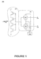
- FIG. 1 illustrates a schematic of a novel power efficient multiplexer, in accordance with embodiments.
- FIG. 2 illustrates a flow chart for a method 200 of selecting one electronic signal from a plurality of electronic signals, in accordance with embodiments.
- FIG. 3 and FIG. 4 illustrate it is possible to stack different numbers of transistors on either or both legs of a stacked inverter in accordance with embodiments.
- Embodiments are described in the context of design and operation of integrated semiconductors. More particularly, embodiments relate to power efficient multiplexers. It is appreciated, however, that embodiments may be utilized in other areas of semiconductor design and operation.
- embodiments are directed toward pFETs (or p-type metal oxide semiconductor field effect transistors (MOSFETS)) formed in surface N-wells and/or nFETs (or n-type MOSFETS) formed in surface P-wells when a p-type substrate and an N-well process are utilized. It is to be appreciated, however, that embodiments are equally applicable to nFETs (or n-type MOSFETS) formed in surface P-wells and/or pFETs (or p-type MOSFETS) formed in surface N-wells when an n-type substrate and a P-well process are utilized. Consequently, embodiments are well suited to semiconductors formed in both p-type and n-type materials, and such embodiments are considered within the scope of the disclosure.
- MOSFETS metal oxide semiconductor field effect transistors
- FIG. 1 illustrates a schematic of a novel power efficient multiplexer 100 , in accordance with embodiments.
- Power efficient multiplexer 100 comprises an inverter 110 and a transmission gate structure 120 .
- Transmission gate structure 120 comprises transmission gates 121 and 122 .
- a bit value in latch 130 determines whether transmission gate 121 is “open” or “closed,” for example whether transmission gate 121 passes a signal or not. Similarly, the bit value in latch 130 determines whether transmission gate 122 passes a signal or not. Both transmission gates 121 and 122 are controlled by the same bit value and that bit value's complement. Consequently, either transmission gate 122 will pass a signal, or transmission gate 121 will pass a signal, but not both simultaneously.
- a zero value in latch 130 will cause transmission gate 121 to pass signal A 125 , while causing transmission gate 122 not to pass any signals. Consequently, transmission gate structure 120 will select signal A 125 corresponding to a zero value in latch 130 .
- a one value in latch 130 will cause transmission gate 122 to pass signal B 126 , while causing transmission gate 121 not to pass any signals. Consequently, transmission gate structure 120 will select signal B 126 corresponding to a one value in latch 130 .
- the signal, A 125 or B 126 , selected by transmission gate structure 120 is inverted by inverter 110 to produce output 140 of power efficient multiplexer 100 .
- static power consumption in modern semiconductor processes e.g., processes with a minimum feature size of about 0.13 microns and smaller, is no longer a negligible component of total power consumption.
- static power may be one-half of total power consumption.
- static power as a percentage of total power, is tending to increase with successive generations of semiconductor process.
- inverter 110 comprises stacked field effect transistors (FETs).
- FETs stacked field effect transistors
- an inverter stage whether conventional or stacked, forms a leakage path, e.g., a series “string” of devices coupled from operating voltage (Vdd) to ground.
- Vdd operating voltage
- static power is consumed by the inverter stage.
- an inverter comprising stacked field effect transistors can consume less static power than a conventional inverter to produce a comparable delay.
- leakage paths within a stacked inverter suffer less leakage than a conventional inverter, yielding additional beneficial leakage reductions.
- a conventional inverter exactly one transistor is on while the other transistor is off. As an unfortunate consequence, approximately the full bias voltage is applied to the off transistor, resulting in a maximum possible leakage for the off transistor.
- each “off” transistor has significantly less than full bias voltage applied. It is appreciated that leakage current generally decreases exponentially as voltage decreases. For example, a factor of two reduction in off bias voltage produces about a factor of eight reduction in leakage current per leakage path.
- leakage induces non zero voltages at intermediate nodes between the off transistors. Such voltages induce body effects in the transistors. Such body effects increase the threshold voltage of the affected transistors. An increased threshold voltage generally produces beneficial decreases in leakage current.
- inverter 110 significantly reduces static power consumption, in comparison to a conventional inverter.
- inverter 110 can be included in inverter 110 in order to achieve differing signal propagation and/or power characteristics, in accordance with embodiments.
- transmission gate structure 120 Also of benefit in reducing power consumption, particularly static power consumption, of power efficient multiplexer 100 is transmission gate structure 120 .
- transmission gates for example transmission gates 121 and 122 , are characterized as having no direct path between power (Vdd) and ground. Consequently, transmission gates are characterized as having extremely small leakage, and thus very little static power consumption.
- a multiplexer can track speed changes of other circuitry of an integrated circuit. For example, if other circuits of an integrated circuit operate faster, generally a multiplexer is required to select a desired signal more quickly in order for the overall circuit to function. Because embodiments comprise stacked devices, they are similar to many logic circuits that also comprise stacked devices, e.g., NAND and/or NOR logic gates. Consequently, embodiments match or track changes in operating speed of complex logic more accurately than multiplexers comprising very simple inverters.
- Embodiments are thus shown to offer significant and highly beneficial improvements in tracking timing changes of other circuits and in static power (leakage current) consumption in comparison to the conventional art.
- FIG. 2 illustrates a flow chart for a method 200 of selecting one electronic signal from a plurality of electronic signals, in accordance with embodiments.
- the plurality of electronic signals is accessed. For example, referring to FIG. 1 , the plurality of electronic signals is accessed at transmission gates 121 and 122 .
- a plurality of transmission gates is configured to select one electronic signal from the plurality of electronic signals. For example, referring to FIG. 1 , a zero value in latch 130 will cause transmission gate 121 to pass signal A 125 , while causing transmission gate 122 not to pass any signals. Consequently, transmission gate structure 120 will select signal A 125 corresponding to a zero value in latch 130 .
- the one electronic signal is inverted utilizing a stacked inverter circuit, for example stacked inverter circuit 110 of FIG. 1 .
Abstract
Description
Claims (20)
Priority Applications (1)
| Application Number | Priority Date | Filing Date | Title |
|---|---|---|---|
| US14/882,264 US9531361B2 (en) | 2004-06-08 | 2015-10-13 | Power efficient multiplexer |
Applications Claiming Priority (11)
| Application Number | Priority Date | Filing Date | Title |
|---|---|---|---|
| US10/864,271 US7336103B1 (en) | 2004-06-08 | 2004-06-08 | Stacked inverter delay chain |
| US11/021,197 US7332931B1 (en) | 2004-06-08 | 2004-12-23 | Leakage efficient anti-glitch filter with variable delay stages |
| US11/021,632 US7498846B1 (en) | 2004-06-08 | 2004-12-23 | Power efficient multiplexer |
| US11/021,221 US7656212B1 (en) | 2004-06-08 | 2004-12-23 | Configurable delay chain with switching control for tail delay elements |
| US11/020,746 US7310008B1 (en) | 2004-06-08 | 2004-12-23 | Configurable delay chain with stacked inverter delay elements |
| US11/021,633 US7330054B1 (en) | 2004-06-08 | 2004-12-23 | Leakage efficient anti-glitch filter |
| US11/021,222 US7635992B1 (en) | 2004-06-08 | 2004-12-23 | Configurable tapered delay chain with multiple sizes of delay elements |
| US12/397,085 US8102190B2 (en) | 2004-06-08 | 2009-03-03 | Power efficient multiplexer |
| US13/356,396 US8587344B2 (en) | 2004-06-08 | 2012-01-23 | Power efficient multiplexer |
| US14/083,348 US9160321B2 (en) | 2004-06-08 | 2013-11-18 | Power efficient multiplexer |
| US14/882,264 US9531361B2 (en) | 2004-06-08 | 2015-10-13 | Power efficient multiplexer |
Related Parent Applications (1)
| Application Number | Title | Priority Date | Filing Date |
|---|---|---|---|
| US14/083,348 Continuation US9160321B2 (en) | 2004-06-08 | 2013-11-18 | Power efficient multiplexer |
Publications (2)
| Publication Number | Publication Date |
|---|---|
| US20160036424A1 US20160036424A1 (en) | 2016-02-04 |
| US9531361B2 true US9531361B2 (en) | 2016-12-27 |
Family
ID=40385387
Family Applications (5)
| Application Number | Title | Priority Date | Filing Date |
|---|---|---|---|
| US11/021,632 Active 2024-09-10 US7498846B1 (en) | 2004-06-08 | 2004-12-23 | Power efficient multiplexer |
| US12/397,085 Active US8102190B2 (en) | 2004-06-08 | 2009-03-03 | Power efficient multiplexer |
| US13/356,396 Active US8587344B2 (en) | 2004-06-08 | 2012-01-23 | Power efficient multiplexer |
| US14/083,348 Active US9160321B2 (en) | 2004-06-08 | 2013-11-18 | Power efficient multiplexer |
| US14/882,264 Active US9531361B2 (en) | 2004-06-08 | 2015-10-13 | Power efficient multiplexer |
Family Applications Before (4)
| Application Number | Title | Priority Date | Filing Date |
|---|---|---|---|
| US11/021,632 Active 2024-09-10 US7498846B1 (en) | 2004-06-08 | 2004-12-23 | Power efficient multiplexer |
| US12/397,085 Active US8102190B2 (en) | 2004-06-08 | 2009-03-03 | Power efficient multiplexer |
| US13/356,396 Active US8587344B2 (en) | 2004-06-08 | 2012-01-23 | Power efficient multiplexer |
| US14/083,348 Active US9160321B2 (en) | 2004-06-08 | 2013-11-18 | Power efficient multiplexer |
Country Status (1)
| Country | Link |
|---|---|
| US (5) | US7498846B1 (en) |
Families Citing this family (7)
| Publication number | Priority date | Publication date | Assignee | Title |
|---|---|---|---|---|
| KR20080026725A (en) * | 2006-09-21 | 2008-03-26 | 주식회사 하이닉스반도체 | Inner signal monitoring device in semiconductor memory device and method for monitoring the same |
| US8461875B1 (en) | 2011-02-18 | 2013-06-11 | Suvolta, Inc. | Digital circuits having improved transistors, and methods therefor |
| JP6297575B2 (en) * | 2013-08-19 | 2018-03-20 | 国立研究開発法人科学技術振興機構 | Reconfigurable delay circuit, delay monitor circuit using the delay circuit, variation correction circuit, variation measurement method, and variation correction method |
| KR102034903B1 (en) * | 2013-10-18 | 2019-10-22 | 매그나칩 반도체 유한회사 | Cmos inverter circuit device |
| US10243558B2 (en) * | 2013-10-18 | 2019-03-26 | Magnachip Semiconductor, Ltd. | Complementary metal-oxide-semiconductor (CMOS) inverter circuit device |
| US9366725B1 (en) | 2015-03-10 | 2016-06-14 | Freescale Semiconductor, Inc. | Multiplexer circuit |
| US9941882B1 (en) | 2016-07-18 | 2018-04-10 | Altera Corporation | Tristate multiplexers with immunity to aging effects |
Citations (163)
| Publication number | Priority date | Publication date | Assignee | Title |
|---|---|---|---|---|
| US3900747A (en) | 1971-12-15 | 1975-08-19 | Sony Corp | Digital circuit for amplifying a signal |
| US3991380A (en) | 1976-02-09 | 1976-11-09 | Rca Corporation | Complementary field effect transistor differential amplifier |
| US4087044A (en) | 1975-12-01 | 1978-05-02 | Siemens Aktiengesellschaft | Circuit arrangement for monitoring the function of a dynamic decoder circuit |
| US4216390A (en) | 1978-10-04 | 1980-08-05 | Rca Corporation | Level shift circuit |
| US4437024A (en) | 1981-10-22 | 1984-03-13 | Rca Corporation | Actively controlled input buffer |
| US4498021A (en) | 1982-07-13 | 1985-02-05 | Matsushita Electric Industrial Co., Ltd. | Booster for transmitting digital signal |
| US4508983A (en) | 1983-02-10 | 1985-04-02 | Motorola, Inc. | MOS Analog switch driven by complementary, minimally skewed clock signals |
| US4568842A (en) | 1983-01-24 | 1986-02-04 | Tokyo Shibaura Denki Kabushiki Kaisha | D-Latch circuit using CMOS transistors |
| US4578600A (en) | 1982-01-26 | 1986-03-25 | Itt Industries, Inc. | CMOS buffer circuit |
| US4651030A (en) | 1983-12-13 | 1987-03-17 | Sharp Kabushiki Kaisha | Decoder circuit for MOS memory of a redundant structure |
| US4700089A (en) | 1984-08-23 | 1987-10-13 | Fujitsu Limited | Delay circuit for gate-array LSI |
| US4739252A (en) | 1986-04-24 | 1988-04-19 | International Business Machines Corporation | Current attenuator useful in a very low leakage current measuring device |
| US4760279A (en) | 1986-07-02 | 1988-07-26 | Kabushiki Kaisha Toshiba | Noise cancelling circuit |
| US4806804A (en) | 1986-03-12 | 1989-02-21 | Deutsche Itt Industries Gmbh | Mosfet integrated delay line for digital signals |
| US4808802A (en) | 1986-08-25 | 1989-02-28 | Hitachi, Ltd. | Method and system for protecting information recorded in information medium |
| US4853560A (en) | 1987-02-06 | 1989-08-01 | Hitachi, Ltd. | Logic circuit and semiconductor integrated circuit device capable of operating by different power supplies |
| US4947064A (en) | 1988-06-09 | 1990-08-07 | Samsung Electronic Co., Ltd. | Semiconductor device having a time delay function |
| JPH0389624A (en) | 1989-08-31 | 1991-04-15 | Fujitsu Ltd | Semiconductor integrated circuit |
| US5039893A (en) | 1984-07-31 | 1991-08-13 | Yamaha Corporation | Signal delay device |
| US5128560A (en) | 1991-03-22 | 1992-07-07 | Micron Technology, Inc. | Boosted supply output driver circuit for driving an all N-channel output stage |
| JPH0491516U (en) | 1990-12-26 | 1992-08-10 | ||
| US5166555A (en) | 1990-05-31 | 1992-11-24 | Nec Corporation | Drive circuit comprising a subsidiary drive circuit |
| US5227679A (en) | 1992-01-02 | 1993-07-13 | Advanced Micro Devices, Inc. | Cmos digital-controlled delay gate |
| US5264738A (en) | 1991-05-31 | 1993-11-23 | U.S. Philips Corp. | Flip-flop circuit having transfer gate delay |
| US5294845A (en) | 1990-12-24 | 1994-03-15 | Motorola, Inc. | Data processor having an output terminal with selectable output impedances |
| US5297086A (en) | 1990-07-31 | 1994-03-22 | Texas Instruments Incorporated | Method for initializing redundant circuitry |
| US5300835A (en) | 1993-02-10 | 1994-04-05 | Cirrus Logic, Inc. | CMOS low power mixed voltage bidirectional I/O buffer |
| JPH06216723A (en) | 1993-01-14 | 1994-08-05 | Toshiba Corp | Semiconductor integrated circuit |
| US5394034A (en) | 1992-07-27 | 1995-02-28 | Siemens Aktiengesellschaft | Programmable logic array having programmable output driver drive capacity |
| US5399925A (en) | 1993-08-02 | 1995-03-21 | Xilinx, Inc. | High-speed tristate inverter |
| US5410278A (en) | 1991-12-19 | 1995-04-25 | Sharp Kabushiki Kaisha | Ring oscillator having a variable oscillating frequency |
| US5414312A (en) | 1993-07-15 | 1995-05-09 | Altera Corporation | Advanced signal driving buffer with directional input transition detection |
| US5455521A (en) | 1993-10-22 | 1995-10-03 | The Board Of Trustees Of The Leland Stanford Junior University | Self-timed interconnect speed-up circuit |
| US5467038A (en) | 1994-02-15 | 1995-11-14 | Hewlett-Packard Company | Quick resolving latch |
| US5497105A (en) | 1994-06-30 | 1996-03-05 | Vlsi Technology, Inc. | Programmable output pad with circuitry for reducing ground bounce noise and power supply noise and method therefor |
| US5521530A (en) | 1994-08-31 | 1996-05-28 | Oki Semiconductor America, Inc. | Efficient method and resulting structure for integrated circuits with flexible I/O interface and power supply voltages |
| US5525616A (en) | 1993-05-13 | 1996-06-11 | Monsanto Company | Method of inhibiting glycolipid synthesis |
| US5568103A (en) | 1994-12-28 | 1996-10-22 | Mitsubishi Electric Engineering Co., Ltd. | Current control circuit of ring oscillator |
| US5587665A (en) | 1995-07-18 | 1996-12-24 | Vlsi Technology, Inc. | Testing hot carrier induced degradation to fall and rise time of CMOS inverter circuits |
| US5594360A (en) | 1994-10-19 | 1997-01-14 | Intel Corporation | Low current reduced area programming voltage detector for flash memory |
| US5606275A (en) | 1995-09-05 | 1997-02-25 | Motorola, Inc. | Buffer circuit having variable output impedance |
| US5610548A (en) | 1995-09-08 | 1997-03-11 | International Business Machines Corporation | Split drive clock buffer |
| US5614845A (en) | 1995-09-08 | 1997-03-25 | International Business Machines Corporation | Independent clock edge regulation |
| US5656963A (en) | 1995-09-08 | 1997-08-12 | International Business Machines Corporation | Clock distribution network for reducing clock skew |
| US5677650A (en) | 1995-12-19 | 1997-10-14 | Pmc-Sierra, Inc. | Ring oscillator having a substantially sinusoidal signal |
| US5680359A (en) | 1995-03-24 | 1997-10-21 | Hyundai Electronics Industries Co., Ltd. | Self-refresh period adjustment circuit for semiconductor memory device |
| US5698994A (en) | 1994-07-29 | 1997-12-16 | Nkk Corporation | Data output circuit, intermediate potential setting circuit, and semiconductor integrated circuit |
| US5739715A (en) | 1995-10-31 | 1998-04-14 | Hewlett-Packard Co. | Digital signal driver circuit having a high slew rate |
| US5764110A (en) | 1996-07-15 | 1998-06-09 | Mitsubishi Denki Kabushiki Kaisha | Voltage controlled ring oscillator stabilized against supply voltage fluctuations |
| US5767700A (en) | 1995-06-30 | 1998-06-16 | Hyundai Electronics Industries Co., Ltd. | Pulse signal transfer unit employing post charge logic |
| US5777488A (en) | 1996-04-19 | 1998-07-07 | Seeq Technology, Inc. | Integrated circuit I/O node useable for configuration input at reset and normal output at other times |
| US5777501A (en) | 1996-04-29 | 1998-07-07 | Mosaid Technologies Incorporated | Digital delay line for a reduced jitter digital delay lock loop |
| US5778214A (en) | 1994-12-09 | 1998-07-07 | Oki Electric Industry Co., Ltd. | Bit-phase aligning circuit |
| US5793222A (en) | 1995-12-26 | 1998-08-11 | Mitsubishi Denki Kabushiki Kaisha | Input circuit |
| US5791715A (en) | 1996-11-22 | 1998-08-11 | Nebel; Michael W. | Extension mechanism for travel trailer slide-out rooms |
| US5793715A (en) | 1995-11-15 | 1998-08-11 | Zen Research N.V. | Methods and apparatus for reducing the access time of an optical drive |
| US5797105A (en) | 1994-08-23 | 1998-08-18 | National Aerospace Laboratory Of Science & Technology | Air active control aircraft using three dimensional true airspeed detection system |
| US5796313A (en) | 1996-04-25 | 1998-08-18 | Waferscale Integration Inc. | Low power programmable ring oscillator |
| US5801548A (en) | 1996-04-11 | 1998-09-01 | Xilinx Inc | Configurable performance-optimized programmable logic device |
| US5811983A (en) | 1996-09-03 | 1998-09-22 | Integrated Device Technology, Inc. | Test ring oscillator |
| US5877632A (en) | 1997-04-11 | 1999-03-02 | Xilinx, Inc. | FPGA with a plurality of I/O voltage levels |
| US5880608A (en) | 1996-12-27 | 1999-03-09 | Intel Corporation | Pulsed domino latches |
| US5894419A (en) | 1997-04-21 | 1999-04-13 | International Business Machines Corporation | System and method for robust clocking schemes for logic circuits |
| US5926050A (en) | 1996-07-29 | 1999-07-20 | Townsend And Townsend And Crew Llp | Separate set/reset paths for time critical signals |
| US5963074A (en) | 1997-06-18 | 1999-10-05 | Credence Systems Corporation | Programmable delay circuit having calibratable delays |
| US5963043A (en) | 1997-09-17 | 1999-10-05 | International Business Machines Corporation | Method and apparatus for characterized parasitic capacitance between integrated-circuit interconnects |
| US5969543A (en) | 1995-09-15 | 1999-10-19 | Xilinx, Inc. | Input signal interface with independently controllable pull-up and pull-down circuitry |
| US5977763A (en) | 1996-02-27 | 1999-11-02 | Micron Technology, Inc. | Circuit and method for measuring and forcing an internal voltage of an integrated circuit |
| US5982211A (en) | 1997-03-31 | 1999-11-09 | Texas Instruments Incorporated | Hybrid dual threshold transistor registers |
| US6011403A (en) | 1997-10-31 | 2000-01-04 | Credence Systems Corporation | Circuit arrangement for measuring leakage current utilizing a differential integrating capacitor |
| US6025738A (en) | 1997-08-22 | 2000-02-15 | International Business Machines Corporation | Gain enhanced split drive buffer |
| US6028490A (en) | 1997-04-25 | 2000-02-22 | Sony Corporation | Ring oscillators having inverting and delay elements |
| US6031403A (en) | 1996-11-13 | 2000-02-29 | International Business Machines Corporation | Pull-up and pull-down circuits |
| US6069506A (en) | 1998-05-20 | 2000-05-30 | Micron Technology, Inc. | Method and apparatus for improving the performance of digital delay locked loop circuits |
| US6111447A (en) * | 1998-05-01 | 2000-08-29 | Vanguard International Semiconductor Corp. | Timing circuit that selectively triggers on a rising or falling input signal edge |
| US6114840A (en) | 1998-09-17 | 2000-09-05 | Integrated Device Technology, Inc. | Signal transfer devices having self-timed booster circuits therein |
| US6127872A (en) | 1997-03-17 | 2000-10-03 | Sony Corporation | Delay circuit and oscillator circuit using the same |
| US6154099A (en) | 1997-10-09 | 2000-11-28 | Kabushiki Kaisha Toshiba | Ring oscillator and method of measuring gate delay time in this ring oscillator |
| US6154100A (en) | 1998-08-31 | 2000-11-28 | Nec Corporation | Ring oscillator and delay circuit using low threshold voltage type MOSFETS |
| US6160755A (en) | 1997-06-17 | 2000-12-12 | Micron Technology, Inc. | Clock signal from an adjustable oscillator for an integrated circuit |
| US6172943B1 (en) | 1997-10-07 | 2001-01-09 | Seiko Instruments Inc. | Electronic clock having an electric power generating element |
| US6172545B1 (en) | 1997-05-09 | 2001-01-09 | Nec Corporation | Delay circuit on a semiconductor device |
| US6188260B1 (en) | 1999-01-22 | 2001-02-13 | Agilent Technologies | Master-slave flip-flop and method |
| US6198334B1 (en) | 1997-04-24 | 2001-03-06 | Hitachi, Ltd. | CMOS circuit |
| US6204710B1 (en) | 1998-06-22 | 2001-03-20 | Xilinx, Inc. | Precision trim circuit for delay lines |
| US20010000426A1 (en) | 1999-01-08 | 2001-04-26 | Altera Corporation | Phase-locked loop or delay-locked loop circuitry for programmable logic devices |
| US6229747B1 (en) | 1998-12-23 | 2001-05-08 | Hyundai Electronics Industries Co., Ltd. | Self-refresh apparatus for a semiconductor memory device |
| US6242936B1 (en) | 1998-08-11 | 2001-06-05 | Texas Instruments Incorporated | Circuit for driving conductive line and testing conductive line for current leakage |
| US6242937B1 (en) | 1999-02-12 | 2001-06-05 | Hyundai Electronics Industries Co., Ltd. | Hot carrier measuring circuit |
| US6262601B1 (en) | 1999-06-25 | 2001-07-17 | Hyundai Electronics Industries Co., Ltd. | Inverter for high voltage full swing output |
| US6275091B1 (en) | 1999-07-23 | 2001-08-14 | Nec Corporation | Clock signal control circuit and method and synchronous delay circuit |
| US6281706B1 (en) | 1998-03-30 | 2001-08-28 | National Semiconductor Corp. | Programmable high speed quiet I/O cell |
| US6285230B1 (en) | 1999-04-07 | 2001-09-04 | Hyundai Electronics Industries Co., Ltd. | Input buffer circuit with adjustable delay via an external power voltage |
| US20010028278A1 (en) | 1995-06-12 | 2001-10-11 | Mitsubishi Denki Kabushiki Kaisha | Temperature dependent circuit, and current generating circuit, inverter and oscillation circuit using the same |
| US20010030561A1 (en) | 2000-02-07 | 2001-10-18 | Hideo Asano | Signal output device and method for sending signals at multiple transfer rates while minimizing crosstalk effects |
| US6321282B1 (en) | 1999-10-19 | 2001-11-20 | Rambus Inc. | Apparatus and method for topography dependent signaling |
| US6323706B1 (en) | 2000-02-24 | 2001-11-27 | Rambus Inc. | Apparatus and method for edge based duty cycle conversion |
| US20010052623A1 (en) | 2000-03-30 | 2001-12-20 | Atsushi Kameyama | Semiconductor integrated circuit |
| US6366115B1 (en) | 2001-02-21 | 2002-04-02 | Analog Devices, Inc. | Buffer circuit with rising and falling edge propagation delay correction and method |
| US6407571B1 (en) | 1999-04-14 | 2002-06-18 | Matsushita Electric Industrial Co., Ltd. | Voltage detecting circuit for a power system |
| US6426641B1 (en) | 1998-10-21 | 2002-07-30 | International Business Machines Corporation | Single pin performance screen ring oscillator with frequency division |
| US6426652B1 (en) | 2001-05-14 | 2002-07-30 | Sun Microsystems, Inc. | Dual-edge triggered dynamic logic |
| US6459319B2 (en) | 2000-05-26 | 2002-10-01 | Fujitsu Limited | Variable delay circuit and semiconductor integrated circuit having the same |
| US6466063B2 (en) | 2001-03-20 | 2002-10-15 | Taiwan Semiconductor Manufacturing Co., Ltd. | Push-pull output buffer with gate voltage feedback loop |
| US6476632B1 (en) | 2000-06-22 | 2002-11-05 | International Business Machines Corporation | Ring oscillator design for MOSFET device reliability investigations and its use for in-line monitoring |
| US20020178415A1 (en) | 2001-03-30 | 2002-11-28 | Ritesh Saraf | Skewed latch flip-flop with embedded scan function |
| US6489796B2 (en) | 2000-06-30 | 2002-12-03 | Mitsubishi Denki Kabushiki Kaisha | Semiconductor device provided with boost circuit consuming less current |
| US20030005775A1 (en) | 2001-07-09 | 2003-01-09 | Nartron Corporation | Compressible capacitance sensor for determining the presence of an object |
| US20030011413A1 (en) | 2001-06-29 | 2003-01-16 | Masleid Robert P. | Low latency clock distribution |
| US20030042960A1 (en) | 2001-08-29 | 2003-03-06 | Gomm Tyler J. | Variable delay circuit and method, and delay locked loop, memory device and computer system using same |
| US6535014B2 (en) | 2000-01-19 | 2003-03-18 | Lucent Technologies, Inc. | Electrical parameter tester having decoupling means |
| US6538471B1 (en) | 2001-10-10 | 2003-03-25 | International Business Machines Corporation | Multi-threshold flip-flop circuit having an outside feedback |
| US6538522B1 (en) | 2001-10-15 | 2003-03-25 | International Business Machines Corporation | Method and ring oscillator for evaluating dynamic circuits |
| US20030057775A1 (en) | 2001-09-26 | 2003-03-27 | Takekazu Yamashita | Semiconductor integrated circuit and multi-chip package |
| US6545519B1 (en) | 2002-03-28 | 2003-04-08 | International Business Machines Corporation | Level shifting, scannable latch, and method therefor |
| US6570407B1 (en) | 2002-01-30 | 2003-05-27 | Sun Microsystems, Inc. | Scannable latch for a dynamic circuit |
| US6573774B1 (en) | 2002-03-25 | 2003-06-03 | Aeroflex Utmc Microelectronic Systems, Inc. | Error correcting latch |
| US6573777B2 (en) | 2001-06-29 | 2003-06-03 | Intel Corporation | Variable-delay element with an inverter and a digitally adjustable resistor |
| US6577157B1 (en) | 1997-11-14 | 2003-06-10 | Altera Corporation | Fully programmable I/O pin with memory |
| US6577176B1 (en) | 2002-06-12 | 2003-06-10 | Fujitsu Limited | Complement reset latch |
| US20030160630A1 (en) | 2002-02-27 | 2003-08-28 | Adrian Earle | Bidirectional edge accelerator circuit |
| US6621318B1 (en) | 2001-06-01 | 2003-09-16 | Sun Microsystems, Inc. | Low voltage latch with uniform sizing |
| US6621298B2 (en) | 1997-10-09 | 2003-09-16 | Lattice Semiconductor Corporation | Variable grain architecture for FPGA integrated circuits |
| US20030189465A1 (en) | 2002-04-09 | 2003-10-09 | International Business Machines Corporation | System and method for measuring circuit performance degradation due to PFET negative bias temperature instability (NBTI) |
| US6657504B1 (en) | 2002-04-30 | 2003-12-02 | Unisys Corporation | System and method of determining ring oscillator speed |
| US6664837B1 (en) | 2002-09-18 | 2003-12-16 | Xilinx, Inc. | Delay line trim unit having consistent performance under varying process and temperature conditions |
| US20030231713A1 (en) | 2002-06-12 | 2003-12-18 | Masleid Robert P. | Complement reset buffer |
| US6690242B2 (en) | 2001-12-21 | 2004-02-10 | Texas Instruments Incorporated | Delay circuit with current steering output symmetry and supply voltage insensitivity |
| US6697929B1 (en) | 2000-02-14 | 2004-02-24 | Intel Corporation | Scannable zero-catcher and one-catcher circuits for reduced clock loading and power dissipation |
| EP1398639A2 (en) | 2002-09-13 | 2004-03-17 | Chartered Semiconductor Manufacturing Pte Ltd. | Test structures for on-chip real-time reliability testing |
| US20040104731A1 (en) | 2002-11-29 | 2004-06-03 | Rolf-P. Vollertsen | Method of reliability testing |
| US20040119503A1 (en) | 2002-12-18 | 2004-06-24 | Shahram Jamshidi | Gate-clocked domino circuits with reduced leakage current |
| US20040119501A1 (en) | 2002-12-23 | 2004-06-24 | Sabbavarapu Anil K. | Scan cell systems and methods |
| US20040124900A1 (en) | 2002-09-11 | 2004-07-01 | Infineon Technologies Ag | Digital signal delay device |
| US6759863B2 (en) | 2000-05-15 | 2004-07-06 | The Governors Of The University Of Alberta | Wireless radio frequency technique design and method for testing of integrated circuits and wafers |
| US6762966B1 (en) | 2003-01-08 | 2004-07-13 | International Business Machines Corporation | Method and circuit to investigate charge transfer array transistor characteristics and aging under realistic stress and its implementation to DRAM MOSFET array transistor |
| US6762638B2 (en) | 2002-10-16 | 2004-07-13 | International Business Machines Corporation | Circuit for preserving data in a flip-flop and a method of use |
| US6768363B2 (en) | 2002-04-03 | 2004-07-27 | Samsung Electronics, Co. Ltd. | Output driver circuit for controlling up-slew rate and down-slew rate independently and up-driving strength and down-driving strength independently |
| US20040148111A1 (en) | 2003-01-23 | 2004-07-29 | Gauthier Claude R. | Embedded integrated circuit aging sensor System |
| US6774734B2 (en) | 2002-11-27 | 2004-08-10 | International Business Machines Corporation | Ring oscillator circuit for EDRAM/DRAM performance monitoring |
| US6798230B1 (en) | 2003-01-15 | 2004-09-28 | Advanced Micro Devices, Inc. | Structure and method for increasing accuracy in predicting hot carrier injection (HCI) degradation in semiconductor devices |
| US6815971B2 (en) | 2002-11-06 | 2004-11-09 | Taiwan Semiconductor Manufacturing Co., Ltd | Method and apparatus for stress testing integrated circuits using an adjustable AC hot carrier injection source |
| US6831494B1 (en) | 2003-05-16 | 2004-12-14 | Transmeta Corporation | Voltage compensated integrated circuits |
| US20040257115A1 (en) | 2003-04-28 | 2004-12-23 | Via Technologies, Inc. | N-domino output latch with accelerated evaluate path |
| US6879200B2 (en) | 2001-03-28 | 2005-04-12 | Fujitsu Limited | Delay circuit, semiconductor integrated circuit device containing a delay circuit and delay method |
| US6882172B1 (en) | 2002-04-16 | 2005-04-19 | Transmeta Corporation | System and method for measuring transistor leakage current with a ring oscillator |
| US6903564B1 (en) | 2003-11-12 | 2005-06-07 | Transmeta Corporation | Device aging determination circuit |
| US6924669B2 (en) | 2000-03-30 | 2005-08-02 | Fujitsu Limited | Output buffer circuit and control method therefor |
| US20050184720A1 (en) | 2003-01-24 | 2005-08-25 | International Business Machines Corporation | Circuitry and methodology to establish correlation between gate dielectric test site reliability and product gate reliability |
| US20050212547A1 (en) | 2002-04-16 | 2005-09-29 | Shingo Suzuki | System and method for measuring time dependent dielectric breakdown with a ring oscillator |
| US6956399B1 (en) | 2004-02-05 | 2005-10-18 | Xilinx, Inc. | High-speed lookup table circuits and methods for programmable logic devices |
| US20050248368A1 (en) | 2003-04-28 | 2005-11-10 | Via Technologies, Inc. | P-domino output latch with accelerated evaluate path |
| US7119580B2 (en) | 2004-06-08 | 2006-10-10 | Transmeta Corporation | Repeater circuit with high performance repeater mode and normal repeater mode |
| US7142018B2 (en) | 2004-06-08 | 2006-11-28 | Transmeta Corporation | Circuits and methods for detecting and assisting wire transitions |
| US7172638B2 (en) | 2002-04-29 | 2007-02-06 | General Motors Corporation | Staged air autothermal reformer for improved startup and operation |
| US7173455B2 (en) | 2004-06-08 | 2007-02-06 | Transmeta Corporation | Repeater circuit having different operating and reset voltage ranges, and methods thereof |
| US7239170B2 (en) | 2003-07-08 | 2007-07-03 | Lsi Corporation | Apparatus and methods for improved input/output cells |
| US7245159B2 (en) | 2004-07-15 | 2007-07-17 | International Business Machines Corporation | Protecting one-hot logic against short-circuits during power-on |
| US7271638B2 (en) | 2003-07-31 | 2007-09-18 | Elpida Memory, Inc. | Delay circuit and delay synchronization loop device |
| US7282958B2 (en) | 2004-01-28 | 2007-10-16 | Samsung Electronics Co., Ltd. | Multiplex (MUX) circuit having a single selection signal and method of generating a MUX output signal with single selection signal |
| US7304503B2 (en) | 2004-06-08 | 2007-12-04 | Transmeta Corporation | Repeater circuit with high performance repeater mode and normal repeater mode, wherein high performance repeater mode has fast reset capability |
| US7336103B1 (en) | 2004-06-08 | 2008-02-26 | Transmeta Corporation | Stacked inverter delay chain |
| US7525341B1 (en) | 2004-09-20 | 2009-04-28 | Marvell Israel (M.I.S.L.) Ltd. | Time-balanced multiplexer switching methods and apparatus |
Family Cites Families (1)
| Publication number | Priority date | Publication date | Assignee | Title |
|---|---|---|---|---|
| JPH0491516A (en) | 1990-08-07 | 1992-03-25 | Seiko Epson Corp | Semiconductor device |
-
2004
- 2004-12-23 US US11/021,632 patent/US7498846B1/en active Active
-
2009
- 2009-03-03 US US12/397,085 patent/US8102190B2/en active Active
-
2012
- 2012-01-23 US US13/356,396 patent/US8587344B2/en active Active
-
2013
- 2013-11-18 US US14/083,348 patent/US9160321B2/en active Active
-
2015
- 2015-10-13 US US14/882,264 patent/US9531361B2/en active Active
Patent Citations (177)
| Publication number | Priority date | Publication date | Assignee | Title |
|---|---|---|---|---|
| US3900747A (en) | 1971-12-15 | 1975-08-19 | Sony Corp | Digital circuit for amplifying a signal |
| US4087044A (en) | 1975-12-01 | 1978-05-02 | Siemens Aktiengesellschaft | Circuit arrangement for monitoring the function of a dynamic decoder circuit |
| US3991380A (en) | 1976-02-09 | 1976-11-09 | Rca Corporation | Complementary field effect transistor differential amplifier |
| US4216390A (en) | 1978-10-04 | 1980-08-05 | Rca Corporation | Level shift circuit |
| US4437024A (en) | 1981-10-22 | 1984-03-13 | Rca Corporation | Actively controlled input buffer |
| US4578600A (en) | 1982-01-26 | 1986-03-25 | Itt Industries, Inc. | CMOS buffer circuit |
| US4498021A (en) | 1982-07-13 | 1985-02-05 | Matsushita Electric Industrial Co., Ltd. | Booster for transmitting digital signal |
| US4568842A (en) | 1983-01-24 | 1986-02-04 | Tokyo Shibaura Denki Kabushiki Kaisha | D-Latch circuit using CMOS transistors |
| US4508983A (en) | 1983-02-10 | 1985-04-02 | Motorola, Inc. | MOS Analog switch driven by complementary, minimally skewed clock signals |
| US4651030A (en) | 1983-12-13 | 1987-03-17 | Sharp Kabushiki Kaisha | Decoder circuit for MOS memory of a redundant structure |
| US5039893A (en) | 1984-07-31 | 1991-08-13 | Yamaha Corporation | Signal delay device |
| US4700089A (en) | 1984-08-23 | 1987-10-13 | Fujitsu Limited | Delay circuit for gate-array LSI |
| US4806804A (en) | 1986-03-12 | 1989-02-21 | Deutsche Itt Industries Gmbh | Mosfet integrated delay line for digital signals |
| US4739252A (en) | 1986-04-24 | 1988-04-19 | International Business Machines Corporation | Current attenuator useful in a very low leakage current measuring device |
| US4760279A (en) | 1986-07-02 | 1988-07-26 | Kabushiki Kaisha Toshiba | Noise cancelling circuit |
| US4808802A (en) | 1986-08-25 | 1989-02-28 | Hitachi, Ltd. | Method and system for protecting information recorded in information medium |
| US4853560A (en) | 1987-02-06 | 1989-08-01 | Hitachi, Ltd. | Logic circuit and semiconductor integrated circuit device capable of operating by different power supplies |
| US4853560B1 (en) | 1987-02-06 | 1993-09-07 | Hitachi, Ltd. | Logic circuit and semiconductor integrated circuit device capable of operating by different power supplies |
| US4947064A (en) | 1988-06-09 | 1990-08-07 | Samsung Electronic Co., Ltd. | Semiconductor device having a time delay function |
| JPH0389624A (en) | 1989-08-31 | 1991-04-15 | Fujitsu Ltd | Semiconductor integrated circuit |
| US5166555A (en) | 1990-05-31 | 1992-11-24 | Nec Corporation | Drive circuit comprising a subsidiary drive circuit |
| US5297086A (en) | 1990-07-31 | 1994-03-22 | Texas Instruments Incorporated | Method for initializing redundant circuitry |
| US5294845A (en) | 1990-12-24 | 1994-03-15 | Motorola, Inc. | Data processor having an output terminal with selectable output impedances |
| JPH0491516U (en) | 1990-12-26 | 1992-08-10 | ||
| US5128560A (en) | 1991-03-22 | 1992-07-07 | Micron Technology, Inc. | Boosted supply output driver circuit for driving an all N-channel output stage |
| US5264738A (en) | 1991-05-31 | 1993-11-23 | U.S. Philips Corp. | Flip-flop circuit having transfer gate delay |
| US5410278A (en) | 1991-12-19 | 1995-04-25 | Sharp Kabushiki Kaisha | Ring oscillator having a variable oscillating frequency |
| US5227679A (en) | 1992-01-02 | 1993-07-13 | Advanced Micro Devices, Inc. | Cmos digital-controlled delay gate |
| US5394034A (en) | 1992-07-27 | 1995-02-28 | Siemens Aktiengesellschaft | Programmable logic array having programmable output driver drive capacity |
| JPH06216723A (en) | 1993-01-14 | 1994-08-05 | Toshiba Corp | Semiconductor integrated circuit |
| US5300835A (en) | 1993-02-10 | 1994-04-05 | Cirrus Logic, Inc. | CMOS low power mixed voltage bidirectional I/O buffer |
| US5525616A (en) | 1993-05-13 | 1996-06-11 | Monsanto Company | Method of inhibiting glycolipid synthesis |
| US5414312A (en) | 1993-07-15 | 1995-05-09 | Altera Corporation | Advanced signal driving buffer with directional input transition detection |
| US5399925A (en) | 1993-08-02 | 1995-03-21 | Xilinx, Inc. | High-speed tristate inverter |
| US5455521A (en) | 1993-10-22 | 1995-10-03 | The Board Of Trustees Of The Leland Stanford Junior University | Self-timed interconnect speed-up circuit |
| US5467038A (en) | 1994-02-15 | 1995-11-14 | Hewlett-Packard Company | Quick resolving latch |
| US5497105A (en) | 1994-06-30 | 1996-03-05 | Vlsi Technology, Inc. | Programmable output pad with circuitry for reducing ground bounce noise and power supply noise and method therefor |
| US5698994A (en) | 1994-07-29 | 1997-12-16 | Nkk Corporation | Data output circuit, intermediate potential setting circuit, and semiconductor integrated circuit |
| US5797105A (en) | 1994-08-23 | 1998-08-18 | National Aerospace Laboratory Of Science & Technology | Air active control aircraft using three dimensional true airspeed detection system |
| US5521530A (en) | 1994-08-31 | 1996-05-28 | Oki Semiconductor America, Inc. | Efficient method and resulting structure for integrated circuits with flexible I/O interface and power supply voltages |
| US5594360A (en) | 1994-10-19 | 1997-01-14 | Intel Corporation | Low current reduced area programming voltage detector for flash memory |
| US5778214A (en) | 1994-12-09 | 1998-07-07 | Oki Electric Industry Co., Ltd. | Bit-phase aligning circuit |
| US5568103A (en) | 1994-12-28 | 1996-10-22 | Mitsubishi Electric Engineering Co., Ltd. | Current control circuit of ring oscillator |
| US5680359A (en) | 1995-03-24 | 1997-10-21 | Hyundai Electronics Industries Co., Ltd. | Self-refresh period adjustment circuit for semiconductor memory device |
| US20010028278A1 (en) | 1995-06-12 | 2001-10-11 | Mitsubishi Denki Kabushiki Kaisha | Temperature dependent circuit, and current generating circuit, inverter and oscillation circuit using the same |
| US5767700A (en) | 1995-06-30 | 1998-06-16 | Hyundai Electronics Industries Co., Ltd. | Pulse signal transfer unit employing post charge logic |
| US5587665A (en) | 1995-07-18 | 1996-12-24 | Vlsi Technology, Inc. | Testing hot carrier induced degradation to fall and rise time of CMOS inverter circuits |
| US5606275A (en) | 1995-09-05 | 1997-02-25 | Motorola, Inc. | Buffer circuit having variable output impedance |
| US5614845A (en) | 1995-09-08 | 1997-03-25 | International Business Machines Corporation | Independent clock edge regulation |
| US5656963A (en) | 1995-09-08 | 1997-08-12 | International Business Machines Corporation | Clock distribution network for reducing clock skew |
| US5610548A (en) | 1995-09-08 | 1997-03-11 | International Business Machines Corporation | Split drive clock buffer |
| US5969543A (en) | 1995-09-15 | 1999-10-19 | Xilinx, Inc. | Input signal interface with independently controllable pull-up and pull-down circuitry |
| US5739715A (en) | 1995-10-31 | 1998-04-14 | Hewlett-Packard Co. | Digital signal driver circuit having a high slew rate |
| US5793715A (en) | 1995-11-15 | 1998-08-11 | Zen Research N.V. | Methods and apparatus for reducing the access time of an optical drive |
| US5677650A (en) | 1995-12-19 | 1997-10-14 | Pmc-Sierra, Inc. | Ring oscillator having a substantially sinusoidal signal |
| US5793222A (en) | 1995-12-26 | 1998-08-11 | Mitsubishi Denki Kabushiki Kaisha | Input circuit |
| US5977763A (en) | 1996-02-27 | 1999-11-02 | Micron Technology, Inc. | Circuit and method for measuring and forcing an internal voltage of an integrated circuit |
| US5801548A (en) | 1996-04-11 | 1998-09-01 | Xilinx Inc | Configurable performance-optimized programmable logic device |
| US5777488A (en) | 1996-04-19 | 1998-07-07 | Seeq Technology, Inc. | Integrated circuit I/O node useable for configuration input at reset and normal output at other times |
| US5796313A (en) | 1996-04-25 | 1998-08-18 | Waferscale Integration Inc. | Low power programmable ring oscillator |
| US5777501A (en) | 1996-04-29 | 1998-07-07 | Mosaid Technologies Incorporated | Digital delay line for a reduced jitter digital delay lock loop |
| US5764110A (en) | 1996-07-15 | 1998-06-09 | Mitsubishi Denki Kabushiki Kaisha | Voltage controlled ring oscillator stabilized against supply voltage fluctuations |
| US5926050A (en) | 1996-07-29 | 1999-07-20 | Townsend And Townsend And Crew Llp | Separate set/reset paths for time critical signals |
| US5811983A (en) | 1996-09-03 | 1998-09-22 | Integrated Device Technology, Inc. | Test ring oscillator |
| US6031403A (en) | 1996-11-13 | 2000-02-29 | International Business Machines Corporation | Pull-up and pull-down circuits |
| US5791715A (en) | 1996-11-22 | 1998-08-11 | Nebel; Michael W. | Extension mechanism for travel trailer slide-out rooms |
| US5880608A (en) | 1996-12-27 | 1999-03-09 | Intel Corporation | Pulsed domino latches |
| US6127872A (en) | 1997-03-17 | 2000-10-03 | Sony Corporation | Delay circuit and oscillator circuit using the same |
| US5982211A (en) | 1997-03-31 | 1999-11-09 | Texas Instruments Incorporated | Hybrid dual threshold transistor registers |
| US6087886A (en) | 1997-03-31 | 2000-07-11 | Texas Instruments Incorporated | Hybrid dual threshold transistor multiplexer |
| US6294930B1 (en) | 1997-04-11 | 2001-09-25 | Xilinx, Inc. | FPGA with a plurality of input reference voltage levels |
| US5877632A (en) | 1997-04-11 | 1999-03-02 | Xilinx, Inc. | FPGA with a plurality of I/O voltage levels |
| US5894419A (en) | 1997-04-21 | 1999-04-13 | International Business Machines Corporation | System and method for robust clocking schemes for logic circuits |
| US6198334B1 (en) | 1997-04-24 | 2001-03-06 | Hitachi, Ltd. | CMOS circuit |
| US6028490A (en) | 1997-04-25 | 2000-02-22 | Sony Corporation | Ring oscillators having inverting and delay elements |
| US6172545B1 (en) | 1997-05-09 | 2001-01-09 | Nec Corporation | Delay circuit on a semiconductor device |
| US6160755A (en) | 1997-06-17 | 2000-12-12 | Micron Technology, Inc. | Clock signal from an adjustable oscillator for an integrated circuit |
| US5963074A (en) | 1997-06-18 | 1999-10-05 | Credence Systems Corporation | Programmable delay circuit having calibratable delays |
| US6025738A (en) | 1997-08-22 | 2000-02-15 | International Business Machines Corporation | Gain enhanced split drive buffer |
| US5963043A (en) | 1997-09-17 | 1999-10-05 | International Business Machines Corporation | Method and apparatus for characterized parasitic capacitance between integrated-circuit interconnects |
| US6172943B1 (en) | 1997-10-07 | 2001-01-09 | Seiko Instruments Inc. | Electronic clock having an electric power generating element |
| US6154099A (en) | 1997-10-09 | 2000-11-28 | Kabushiki Kaisha Toshiba | Ring oscillator and method of measuring gate delay time in this ring oscillator |
| US6621298B2 (en) | 1997-10-09 | 2003-09-16 | Lattice Semiconductor Corporation | Variable grain architecture for FPGA integrated circuits |
| US6011403A (en) | 1997-10-31 | 2000-01-04 | Credence Systems Corporation | Circuit arrangement for measuring leakage current utilizing a differential integrating capacitor |
| US6577157B1 (en) | 1997-11-14 | 2003-06-10 | Altera Corporation | Fully programmable I/O pin with memory |
| US6281706B1 (en) | 1998-03-30 | 2001-08-28 | National Semiconductor Corp. | Programmable high speed quiet I/O cell |
| US6111447A (en) * | 1998-05-01 | 2000-08-29 | Vanguard International Semiconductor Corp. | Timing circuit that selectively triggers on a rising or falling input signal edge |
| US6069506A (en) | 1998-05-20 | 2000-05-30 | Micron Technology, Inc. | Method and apparatus for improving the performance of digital delay locked loop circuits |
| US6204710B1 (en) | 1998-06-22 | 2001-03-20 | Xilinx, Inc. | Precision trim circuit for delay lines |
| US6242936B1 (en) | 1998-08-11 | 2001-06-05 | Texas Instruments Incorporated | Circuit for driving conductive line and testing conductive line for current leakage |
| US6154100A (en) | 1998-08-31 | 2000-11-28 | Nec Corporation | Ring oscillator and delay circuit using low threshold voltage type MOSFETS |
| US6114840A (en) | 1998-09-17 | 2000-09-05 | Integrated Device Technology, Inc. | Signal transfer devices having self-timed booster circuits therein |
| US6426641B1 (en) | 1998-10-21 | 2002-07-30 | International Business Machines Corporation | Single pin performance screen ring oscillator with frequency division |
| US6229747B1 (en) | 1998-12-23 | 2001-05-08 | Hyundai Electronics Industries Co., Ltd. | Self-refresh apparatus for a semiconductor memory device |
| US20010000426A1 (en) | 1999-01-08 | 2001-04-26 | Altera Corporation | Phase-locked loop or delay-locked loop circuitry for programmable logic devices |
| US6188260B1 (en) | 1999-01-22 | 2001-02-13 | Agilent Technologies | Master-slave flip-flop and method |
| US6242937B1 (en) | 1999-02-12 | 2001-06-05 | Hyundai Electronics Industries Co., Ltd. | Hot carrier measuring circuit |
| US6285230B1 (en) | 1999-04-07 | 2001-09-04 | Hyundai Electronics Industries Co., Ltd. | Input buffer circuit with adjustable delay via an external power voltage |
| US6407571B1 (en) | 1999-04-14 | 2002-06-18 | Matsushita Electric Industrial Co., Ltd. | Voltage detecting circuit for a power system |
| US6262601B1 (en) | 1999-06-25 | 2001-07-17 | Hyundai Electronics Industries Co., Ltd. | Inverter for high voltage full swing output |
| US6275091B1 (en) | 1999-07-23 | 2001-08-14 | Nec Corporation | Clock signal control circuit and method and synchronous delay circuit |
| US6321282B1 (en) | 1999-10-19 | 2001-11-20 | Rambus Inc. | Apparatus and method for topography dependent signaling |
| US20020056016A1 (en) | 1999-10-19 | 2002-05-09 | Rambus Inc. | Apparatus and method for topography dependent signaling |
| US6535014B2 (en) | 2000-01-19 | 2003-03-18 | Lucent Technologies, Inc. | Electrical parameter tester having decoupling means |
| US20010030561A1 (en) | 2000-02-07 | 2001-10-18 | Hideo Asano | Signal output device and method for sending signals at multiple transfer rates while minimizing crosstalk effects |
| US6697929B1 (en) | 2000-02-14 | 2004-02-24 | Intel Corporation | Scannable zero-catcher and one-catcher circuits for reduced clock loading and power dissipation |
| US6323706B1 (en) | 2000-02-24 | 2001-11-27 | Rambus Inc. | Apparatus and method for edge based duty cycle conversion |
| US7053660B2 (en) | 2000-03-30 | 2006-05-30 | Fujitsu Limited | Output buffer circuit and control method therefor |
| US6455901B2 (en) | 2000-03-30 | 2002-09-24 | Kabushiki Kaisha Toshiba | Semiconductor integrated circuit |
| US20010052623A1 (en) | 2000-03-30 | 2001-12-20 | Atsushi Kameyama | Semiconductor integrated circuit |
| US6924669B2 (en) | 2000-03-30 | 2005-08-02 | Fujitsu Limited | Output buffer circuit and control method therefor |
| US6759863B2 (en) | 2000-05-15 | 2004-07-06 | The Governors Of The University Of Alberta | Wireless radio frequency technique design and method for testing of integrated circuits and wafers |
| US6459319B2 (en) | 2000-05-26 | 2002-10-01 | Fujitsu Limited | Variable delay circuit and semiconductor integrated circuit having the same |
| US6476632B1 (en) | 2000-06-22 | 2002-11-05 | International Business Machines Corporation | Ring oscillator design for MOSFET device reliability investigations and its use for in-line monitoring |
| US6489796B2 (en) | 2000-06-30 | 2002-12-03 | Mitsubishi Denki Kabushiki Kaisha | Semiconductor device provided with boost circuit consuming less current |
| US6366115B1 (en) | 2001-02-21 | 2002-04-02 | Analog Devices, Inc. | Buffer circuit with rising and falling edge propagation delay correction and method |
| US6466063B2 (en) | 2001-03-20 | 2002-10-15 | Taiwan Semiconductor Manufacturing Co., Ltd. | Push-pull output buffer with gate voltage feedback loop |
| US6879200B2 (en) | 2001-03-28 | 2005-04-12 | Fujitsu Limited | Delay circuit, semiconductor integrated circuit device containing a delay circuit and delay method |
| US20020178415A1 (en) | 2001-03-30 | 2002-11-28 | Ritesh Saraf | Skewed latch flip-flop with embedded scan function |
| US6426652B1 (en) | 2001-05-14 | 2002-07-30 | Sun Microsystems, Inc. | Dual-edge triggered dynamic logic |
| US6621318B1 (en) | 2001-06-01 | 2003-09-16 | Sun Microsystems, Inc. | Low voltage latch with uniform sizing |
| US20030011413A1 (en) | 2001-06-29 | 2003-01-16 | Masleid Robert P. | Low latency clock distribution |
| US6573777B2 (en) | 2001-06-29 | 2003-06-03 | Intel Corporation | Variable-delay element with an inverter and a digitally adjustable resistor |
| US20030005775A1 (en) | 2001-07-09 | 2003-01-09 | Nartron Corporation | Compressible capacitance sensor for determining the presence of an object |
| US20030042960A1 (en) | 2001-08-29 | 2003-03-06 | Gomm Tyler J. | Variable delay circuit and method, and delay locked loop, memory device and computer system using same |
| US20030057775A1 (en) | 2001-09-26 | 2003-03-27 | Takekazu Yamashita | Semiconductor integrated circuit and multi-chip package |
| US6538471B1 (en) | 2001-10-10 | 2003-03-25 | International Business Machines Corporation | Multi-threshold flip-flop circuit having an outside feedback |
| US6538522B1 (en) | 2001-10-15 | 2003-03-25 | International Business Machines Corporation | Method and ring oscillator for evaluating dynamic circuits |
| US6690242B2 (en) | 2001-12-21 | 2004-02-10 | Texas Instruments Incorporated | Delay circuit with current steering output symmetry and supply voltage insensitivity |
| US6570407B1 (en) | 2002-01-30 | 2003-05-27 | Sun Microsystems, Inc. | Scannable latch for a dynamic circuit |
| US20030160630A1 (en) | 2002-02-27 | 2003-08-28 | Adrian Earle | Bidirectional edge accelerator circuit |
| US6573774B1 (en) | 2002-03-25 | 2003-06-03 | Aeroflex Utmc Microelectronic Systems, Inc. | Error correcting latch |
| US6545519B1 (en) | 2002-03-28 | 2003-04-08 | International Business Machines Corporation | Level shifting, scannable latch, and method therefor |
| US6768363B2 (en) | 2002-04-03 | 2004-07-27 | Samsung Electronics, Co. Ltd. | Output driver circuit for controlling up-slew rate and down-slew rate independently and up-driving strength and down-driving strength independently |
| US6731179B2 (en) | 2002-04-09 | 2004-05-04 | International Business Machines Corporation | System and method for measuring circuit performance degradation due to PFET negative bias temperature instability (NBTI) |
| US20030189465A1 (en) | 2002-04-09 | 2003-10-09 | International Business Machines Corporation | System and method for measuring circuit performance degradation due to PFET negative bias temperature instability (NBTI) |
| US6882172B1 (en) | 2002-04-16 | 2005-04-19 | Transmeta Corporation | System and method for measuring transistor leakage current with a ring oscillator |
| US20050212547A1 (en) | 2002-04-16 | 2005-09-29 | Shingo Suzuki | System and method for measuring time dependent dielectric breakdown with a ring oscillator |
| US6885210B1 (en) | 2002-04-16 | 2005-04-26 | Transmeta Corporation | System and method for measuring transistor leakage current with a ring oscillator with backbias controls |
| US7172638B2 (en) | 2002-04-29 | 2007-02-06 | General Motors Corporation | Staged air autothermal reformer for improved startup and operation |
| US6657504B1 (en) | 2002-04-30 | 2003-12-02 | Unisys Corporation | System and method of determining ring oscillator speed |
| US7053680B2 (en) | 2002-06-12 | 2006-05-30 | Fujitsu Limited | Complement reset buffer |
| US20030231713A1 (en) | 2002-06-12 | 2003-12-18 | Masleid Robert P. | Complement reset buffer |
| US6731140B2 (en) | 2002-06-12 | 2004-05-04 | Fujitsu Limited | Complement reset multiplexer latch |
| US6577176B1 (en) | 2002-06-12 | 2003-06-10 | Fujitsu Limited | Complement reset latch |
| US20040124900A1 (en) | 2002-09-11 | 2004-07-01 | Infineon Technologies Ag | Digital signal delay device |
| US6724214B2 (en) | 2002-09-13 | 2004-04-20 | Chartered Semiconductor Manufacturing Ltd. | Test structures for on-chip real-time reliability testing |
| EP1398639A2 (en) | 2002-09-13 | 2004-03-17 | Chartered Semiconductor Manufacturing Pte Ltd. | Test structures for on-chip real-time reliability testing |
| US6664837B1 (en) | 2002-09-18 | 2003-12-16 | Xilinx, Inc. | Delay line trim unit having consistent performance under varying process and temperature conditions |
| US6762638B2 (en) | 2002-10-16 | 2004-07-13 | International Business Machines Corporation | Circuit for preserving data in a flip-flop and a method of use |
| US6815971B2 (en) | 2002-11-06 | 2004-11-09 | Taiwan Semiconductor Manufacturing Co., Ltd | Method and apparatus for stress testing integrated circuits using an adjustable AC hot carrier injection source |
| US6774734B2 (en) | 2002-11-27 | 2004-08-10 | International Business Machines Corporation | Ring oscillator circuit for EDRAM/DRAM performance monitoring |
| US20040104731A1 (en) | 2002-11-29 | 2004-06-03 | Rolf-P. Vollertsen | Method of reliability testing |
| US20040119503A1 (en) | 2002-12-18 | 2004-06-24 | Shahram Jamshidi | Gate-clocked domino circuits with reduced leakage current |
| US6815977B2 (en) | 2002-12-23 | 2004-11-09 | Intel Corporation | Scan cell systems and methods |
| US20040119501A1 (en) | 2002-12-23 | 2004-06-24 | Sabbavarapu Anil K. | Scan cell systems and methods |
| US6762966B1 (en) | 2003-01-08 | 2004-07-13 | International Business Machines Corporation | Method and circuit to investigate charge transfer array transistor characteristics and aging under realistic stress and its implementation to DRAM MOSFET array transistor |
| US6798230B1 (en) | 2003-01-15 | 2004-09-28 | Advanced Micro Devices, Inc. | Structure and method for increasing accuracy in predicting hot carrier injection (HCI) degradation in semiconductor devices |
| US20040148111A1 (en) | 2003-01-23 | 2004-07-29 | Gauthier Claude R. | Embedded integrated circuit aging sensor System |
| US20050184720A1 (en) | 2003-01-24 | 2005-08-25 | International Business Machines Corporation | Circuitry and methodology to establish correlation between gate dielectric test site reliability and product gate reliability |
| US20040257115A1 (en) | 2003-04-28 | 2004-12-23 | Via Technologies, Inc. | N-domino output latch with accelerated evaluate path |
| US20050248368A1 (en) | 2003-04-28 | 2005-11-10 | Via Technologies, Inc. | P-domino output latch with accelerated evaluate path |
| US6831494B1 (en) | 2003-05-16 | 2004-12-14 | Transmeta Corporation | Voltage compensated integrated circuits |
| US7239170B2 (en) | 2003-07-08 | 2007-07-03 | Lsi Corporation | Apparatus and methods for improved input/output cells |
| US7271638B2 (en) | 2003-07-31 | 2007-09-18 | Elpida Memory, Inc. | Delay circuit and delay synchronization loop device |
| US6903564B1 (en) | 2003-11-12 | 2005-06-07 | Transmeta Corporation | Device aging determination circuit |
| US7282958B2 (en) | 2004-01-28 | 2007-10-16 | Samsung Electronics Co., Ltd. | Multiplex (MUX) circuit having a single selection signal and method of generating a MUX output signal with single selection signal |
| US6956399B1 (en) | 2004-02-05 | 2005-10-18 | Xilinx, Inc. | High-speed lookup table circuits and methods for programmable logic devices |
| US7142018B2 (en) | 2004-06-08 | 2006-11-28 | Transmeta Corporation | Circuits and methods for detecting and assisting wire transitions |
| US7119580B2 (en) | 2004-06-08 | 2006-10-10 | Transmeta Corporation | Repeater circuit with high performance repeater mode and normal repeater mode |
| US7173455B2 (en) | 2004-06-08 | 2007-02-06 | Transmeta Corporation | Repeater circuit having different operating and reset voltage ranges, and methods thereof |
| US7295041B1 (en) | 2004-06-08 | 2007-11-13 | Transmeta Corporation | Circuits and methods for detecting and assisting wire transitions |
| US7304503B2 (en) | 2004-06-08 | 2007-12-04 | Transmeta Corporation | Repeater circuit with high performance repeater mode and normal repeater mode, wherein high performance repeater mode has fast reset capability |
| US7336103B1 (en) | 2004-06-08 | 2008-02-26 | Transmeta Corporation | Stacked inverter delay chain |
| US7245159B2 (en) | 2004-07-15 | 2007-07-17 | International Business Machines Corporation | Protecting one-hot logic against short-circuits during power-on |
| US7525341B1 (en) | 2004-09-20 | 2009-04-28 | Marvell Israel (M.I.S.L.) Ltd. | Time-balanced multiplexer switching methods and apparatus |
| US7808271B2 (en) | 2004-09-20 | 2010-10-05 | Marvell Israel (M.I.S.L.) Ltd. | Time-balanced multiplexer switching methods and apparatus |
Non-Patent Citations (10)
| Title |
|---|
| Chen, G et al., "Dynamic NBTI of p-MOS Transistors and its Impact on MOSFET Scaling" IEEE Electron Device Letters, Dec. 2002, pp. 1-3. |
| Lima T., et al.; "Capacitance Coupling Immune, Transient Sensitive Accelerator for Resistive Interconnect Signals of Subquater Micron ULSI", IEEE Journal of Solid-State Circuits, IEEE Inc., New York, US, vol. 31, No. 4, Apr. 1996, pp. 531-536. |
| Nalamalpu, et al., "Boosters for Driving Long OnChip Interconnects-Design Issues, Interconnect Synthesis, and Comparision With Repeaters", Jan. 2002, IEEE Transactions on Computer-Aided Design of Integrated Circuits and Systems, vol. 21, No. 1, Jan. 2002, pp. 50-62. |
| Oner et al., "A compact Monitoring Circuit for Real-Time On-Chip Diagnosis of Hot-Carrier Induced Degradation" Microelectronic test structures. Proceedings, IEEE International Conference in Monterey, CA. Mar. 17, 1997-Mar. 20, 1997, pp. 72-76. |
| Peters, Laura. "NBTI: A Growing Threat to Device Reliability," Semiconductor International. Mar. 1, 2004 Http://www.reed-electronics.com/semiconductor/article/CA386329?industryid=3033. |
| Reddy. V. et al., "Impact of Negative Bias Temperature Instability on Digital Circuit Reliability". 2002 IEE International Reliability Physics Symposium Proceedings, Dallas, TX Apr. 7, 2002-Apr. 11, 2002, pp. 248-254. |
| Rhyne, "Fundamentals of Digital Systems Design", N.J., Jan. 1973, pp. 70-71. |
| Ryohei Kaneda, Translation of Japanese Kokai Patent Application No. HEI 3[1991]-89624, publication date: Apr. 15, 1991, pp. 1-6. |
| Stojanovic, V. and Oklobdzija, V., "Comparative Analysis of Master-Slave Latches and Flip-Flops for High-Performance and Low-Power Systems", IEEE Journal of Solid-State Circuits, vol. 34, No. 4, Apr. 1999, pp. 536-548. |
| Taub, et al., Digital Integrated Electronics, Jan. 1977, McGraw-Hill, Inc. pp. 98-100. |
Also Published As
| Publication number | Publication date |
|---|---|
| US20160036424A1 (en) | 2016-02-04 |
| US9160321B2 (en) | 2015-10-13 |
| US20120242371A1 (en) | 2012-09-27 |
| US8587344B2 (en) | 2013-11-19 |
| US7498846B1 (en) | 2009-03-03 |
| US20090219053A1 (en) | 2009-09-03 |
| US8102190B2 (en) | 2012-01-24 |
| US20140070848A1 (en) | 2014-03-13 |
Similar Documents
| Publication | Publication Date | Title |
|---|---|---|
| US9531361B2 (en) | Power efficient multiplexer | |
| US7332931B1 (en) | Leakage efficient anti-glitch filter with variable delay stages | |
| Koo et al. | A new level-up shifter for high speed and wide range interface in ultra deep sub-micron | |
| US6225846B1 (en) | Body voltage controlled semiconductor integrated circuit | |
| US7468615B1 (en) | Voltage level shifter | |
| US20070120578A1 (en) | Integrated Header Switch with Low-Leakage PMOS and High-Leakage NMOS Transistors | |
| US7605636B2 (en) | Power gating structure, semiconductor including the same and method of controlling a power gating | |
| US7102410B2 (en) | High voltage level converter using low voltage devices | |
| US6373291B1 (en) | Pass transistor logic circuit for reducing power consumption | |
| US7592842B2 (en) | Configurable delay chain with stacked inverter delay elements | |
| US7030643B2 (en) | Output buffer circuits including logic gates having balanced output nodes | |
| US8638122B2 (en) | Apparatus for metastability-hardened storage circuits and associated methods | |
| Rao et al. | Circuit techniques for gate and sub-threshold leakage minimization in future CMOS technologies | |
| US7205830B2 (en) | Analog MOS circuits having reduced voltage stress | |
| US7352228B2 (en) | Method and apparatus of a level shifter circuit with duty-cycle correction | |
| US7656212B1 (en) | Configurable delay chain with switching control for tail delay elements | |
| US6225830B1 (en) | Differential mode logic gate having NAND and NOR portions to produce complementary outputs | |
| US7635992B1 (en) | Configurable tapered delay chain with multiple sizes of delay elements | |
| JPH09214324A (en) | Cmos logic circuit | |
| US6995586B2 (en) | Monotonic leakage-tolerant logic circuits | |
| US10911048B1 (en) | Dynamically adjustable CMOS circuit | |
| JP2000196436A (en) | Input output circuit for semiconductor integrated circuit device | |
| CN113328741B (en) | P-type semi-stacked sub-threshold standard unit based on Schmitt trigger circuit | |
| US10855261B2 (en) | Level shifter with deterministic output during power-up sequence | |
| Amarchinta et al. | Robust and high performance subthreshold standard cell design |
Legal Events
| Date | Code | Title | Description |
|---|---|---|---|
| STCF | Information on status: patent grant |
Free format text: PATENTED CASE |
|
| AS | Assignment |
Owner name: INTELLECTUAL VENTURE FUNDING LLC, NEVADA Free format text: ASSIGNMENT OF ASSIGNORS INTEREST;ASSIGNOR:TRANSMETA LLC;REEL/FRAME:044037/0039 Effective date: 20090128 |
|
| AS | Assignment |
Owner name: INTELLECTUAL VENTURES HOLDING 81 LLC, CALIFORNIA Free format text: MERGER;ASSIGNOR:INTELLECTUAL VENTURE FUNDING LLC;REEL/FRAME:044097/0001 Effective date: 20150827 |
|
| AS | Assignment |
Owner name: INTELLECTUAL VENTURES HOLDING 81 LLC, NEVADA Free format text: CORRECTIVE ASSIGNMENT TO CORRECT THE STATE IN ASSIGNEE ADDRESS PREVIOUSLY RECORDED AT REEL: 044097 FRAME: 0001. ASSIGNOR(S) HEREBY CONFIRMS THE MERGER;ASSIGNOR:INTELLECTUAL VENTURE FUNDING LLC;REEL/FRAME:046245/0753 Effective date: 20150827 |
|
| MAFP | Maintenance fee payment |
Free format text: PAYMENT OF MAINTENANCE FEE, 4TH YEAR, LARGE ENTITY (ORIGINAL EVENT CODE: M1551); ENTITY STATUS OF PATENT OWNER: LARGE ENTITY Year of fee payment: 4 |