US9276830B2 - Secure electronic element network - Google Patents
Secure electronic element network Download PDFInfo
- Publication number
- US9276830B2 US9276830B2 US13/478,383 US201213478383A US9276830B2 US 9276830 B2 US9276830 B2 US 9276830B2 US 201213478383 A US201213478383 A US 201213478383A US 9276830 B2 US9276830 B2 US 9276830B2
- Authority
- US
- United States
- Prior art keywords
- electronic element
- electronic
- primary
- network
- data
- Prior art date
- Legal status (The legal status is an assumption and is not a legal conclusion. Google has not performed a legal analysis and makes no representation as to the accuracy of the status listed.)
- Expired - Fee Related, expires
Links
- 230000004044 response Effects 0.000 claims abstract description 72
- 230000015654 memory Effects 0.000 claims description 57
- 238000004891 communication Methods 0.000 claims description 35
- 238000000034 method Methods 0.000 claims description 8
- 230000006870 function Effects 0.000 claims description 7
- 230000005540 biological transmission Effects 0.000 claims 6
- 230000007704 transition Effects 0.000 claims 2
- 238000012545 processing Methods 0.000 description 8
- 239000004593 Epoxy Substances 0.000 description 1
- 230000009471 action Effects 0.000 description 1
- 230000008859 change Effects 0.000 description 1
- 238000004590 computer program Methods 0.000 description 1
- 238000005516 engineering process Methods 0.000 description 1
- 238000004519 manufacturing process Methods 0.000 description 1
- 230000007246 mechanism Effects 0.000 description 1
- 238000012544 monitoring process Methods 0.000 description 1
- 230000003287 optical effect Effects 0.000 description 1
- 230000008569 process Effects 0.000 description 1
- 239000011253 protective coating Substances 0.000 description 1
- 238000007789 sealing Methods 0.000 description 1
- 238000012360 testing method Methods 0.000 description 1
- 238000005406 washing Methods 0.000 description 1
Images


Classifications
-
- H—ELECTRICITY
- H04—ELECTRIC COMMUNICATION TECHNIQUE
- H04L—TRANSMISSION OF DIGITAL INFORMATION, e.g. TELEGRAPHIC COMMUNICATION
- H04L43/00—Arrangements for monitoring or testing data switching networks
- H04L43/08—Monitoring or testing based on specific metrics, e.g. QoS, energy consumption or environmental parameters
- H04L43/0805—Monitoring or testing based on specific metrics, e.g. QoS, energy consumption or environmental parameters by checking availability
- H04L43/0817—Monitoring or testing based on specific metrics, e.g. QoS, energy consumption or environmental parameters by checking availability by checking functioning
-
- H—ELECTRICITY
- H04—ELECTRIC COMMUNICATION TECHNIQUE
- H04L—TRANSMISSION OF DIGITAL INFORMATION, e.g. TELEGRAPHIC COMMUNICATION
- H04L41/00—Arrangements for maintenance, administration or management of data switching networks, e.g. of packet switching networks
- H04L41/06—Management of faults, events, alarms or notifications
- H04L41/0654—Management of faults, events, alarms or notifications using network fault recovery
-
- Y—GENERAL TAGGING OF NEW TECHNOLOGICAL DEVELOPMENTS; GENERAL TAGGING OF CROSS-SECTIONAL TECHNOLOGIES SPANNING OVER SEVERAL SECTIONS OF THE IPC; TECHNICAL SUBJECTS COVERED BY FORMER USPC CROSS-REFERENCE ART COLLECTIONS [XRACs] AND DIGESTS
- Y04—INFORMATION OR COMMUNICATION TECHNOLOGIES HAVING AN IMPACT ON OTHER TECHNOLOGY AREAS
- Y04S—SYSTEMS INTEGRATING TECHNOLOGIES RELATED TO POWER NETWORK OPERATION, COMMUNICATION OR INFORMATION TECHNOLOGIES FOR IMPROVING THE ELECTRICAL POWER GENERATION, TRANSMISSION, DISTRIBUTION, MANAGEMENT OR USAGE, i.e. SMART GRIDS
- Y04S40/00—Systems for electrical power generation, transmission, distribution or end-user application management characterised by the use of communication or information technologies, or communication or information technology specific aspects supporting them
-
- Y04S40/166—
-
- Y04S40/168—
Definitions
- This disclosure relates to a network of electronic elements in an electronic device. More specifically, this disclosure relates to securely ensuring the proper functioning of a network of electronic elements in an electronic device.
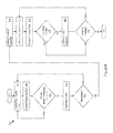
- FIG. 1 shows an exemplary network of secure electronic elements.
- FIG. 2 shows an exemplary network of secure electronic elements.
- FIG. 3 shows an example of logic that electronic elements may execute to secure a network.
- FIG. 4 shows an example of logic that an electronic element may execute to the secure a network.
- FIG. 1 shows an exemplary network of secure electronic elements 100 .
- a network of secure electronic elements 100 may include electronic elements (e.g., 101 - 104 ) that implement, at least in part, an electronic device.
- the electronic device implemented by the network of secure electronic elements 100 may be a laptop, desktop, or other type of computer, a personal data assistant, or a portable email device.
- Additional examples of electronic devices include televisions, stereo equipment such as amplifiers, pre-amplifiers, and tuners, home media devices such as compact disc (CD)/digital versatile disc (DVD) players, portable MP3 players, high definition (e.g., Blu-RayTM or DVD audio) media players, or home media servers.
- CD compact disc
- DVD digital versatile disc
- portable MP3 players portable MP3 players
- high definition e.g., Blu-RayTM or DVD audio
- electronic devices include vehicles such as cars and planes, societal infrastructure such as power plants, traffic monitoring and control systems, or radio and television broadcasting systems. Further examples include home climate control systems, washing machines, refrigerators and freezers, dishwashers, intrusion alarms, audio/video surveillance or security equipment, network attached storage, and network routers and gateways.
- the electronic devices may be found in virtually any context, including the home, business, public spaces, or automobile.
- the electronic devices may further include automobile engine controllers, audio head ends or DVD players, satellite music transceivers, noise cancellation systems, voice recognition systems, climate control systems, navigation systems, alarm systems, or other devices.
- the network of secure electronic elements 100 includes electronic elements, such as a WiFi Controller 101 , a Central Processing Unit (CPU) 102 , a Graphical Processing Unit (GPU) 103 , and a Memory Controller 104 .
- the electronic elements e.g., 101 - 104
- the electronic elements may implement, at least in part, one of the electronic devices listed above.
- the electronic elements may vary widely in form, function, and complexity.
- the electronic elements may further include input/output interfaces (e.g., Universal Serial Bus (USB)) interfaces, clock or timer logic, programmable voltage regulators, flash memory interfaces, or firmware ROMs (e.g., a basic input/output system (BIOS) ROM.
- input/output interfaces e.g., Universal Serial Bus (USB)
- clock or timer logic e.g., programmable voltage regulators
- flash memory interfaces e.g., a basic input/output system (BIOS) ROM.
- firmware ROMs e.g., a basic input/output system (BIOS) ROM.
- the electronic elements may include an engine controller, a global positioning system (GPS) navigation system, an audio processing computer, and a climate control computer.
- GPS global positioning system
- audio processing computer e.g., a climate control computer.
- Each of the electronic elements may include a secure element (e.g., 111 - 114 ).
- the secure element e.g., 111 - 114
- the secure element may work together to secure the network of secure electronic elements 100 by determining whether each electronic element is functioning properly.
- a secure element e.g., 111 - 114
- the secure element (e.g., 111 - 114 ) may be separate from, but in communication with, the electronic element (e.g., 101 - 104 ).
- the secure element associated with an electronic element may also control or alter the electronic element's functional capability.
- a secure element may slow the clock speed of a CPU 102 or a GPU 103 , disable wireless radios of a WiFi Controller 101 , or power down or shut down the electronic element.
- the network of secure electronic elements 100 may include master electronic elements and slave electronic elements.
- a master electronic element may check, at defined times, whether a selected slave electronic element is functioning properly.
- the master electronic element may check whether some or all of the slave electronic elements within the network of secure electronic elements 100 are functioning properly.
- the WiFi Controller 101 is a master electronic element.
- the CPU 102 , the GPU 103 , and the Memory Controller 104 are each slave electronic elements.
- a master electronic element may include a Secure Master Element (e.g., 111 ) while the slave electronic elements (e.g., 102 - 104 ) may each include a Secure Slave Element (e.g., 112 - 114 ).
- the master electronic element e.g., the WiFi Controller 101
- the WiFi Controller 101 may include a Secure Master Element 111 .
- the Secure Master Element 111 may include a Secure Communication Interface 120 in communication with a Secure Processor 130 and a Secure Memory 140 .
- the Secure Memory 140 of the Secure Master Element 111 may store a Secure Network Element List 151 , Secure Check Parameters 152 , Counter Responses 153 , and Secure Master Element Logic 154 .
- the Secure Master Element Logic 154 may be stored as processor executable instructions that when executed by the secure processor 130 determine whether selected slave electronic elements are functioning properly as well as to react accordingly.
- the Secure Master Element 111 may direct the WiFi Controller 101 to act as the master electronic element of the network of secure electronic elements 100 .
- the Secure Master Element Logic 154 may select which slave electronic elements to check by reading the Secure Network Element List 151 .
- the Secure Network Element List 151 may list the CPU 102 , the GPU 103 , the Memory Controller 104 , or any other electronic elements in the network 100 as slave electronic elements. In other words, the Secure Master Element Logic 154 may check whether any specified elements in the secure network element list 151 are functioning properly.
- the Secure Master Element Logic 154 may determine whether the CPU 102 , the GPU 103 , and the Memory Controller 104 (the slave electronic elements) are functioning properly by utilizing the Secure Check Parameters 152 .
- the Secure Check Parameters 152 may include the proper response that the check to each of the slave electronic elements should respectively return.
- the Secure Check Parameters 152 may specify that the proper response from checks to the Memory Controller 104 should be a “Yes” response.
- the Secure Check Parameters 152 may also specify more complex responses (e.g., a sequence of data or messages, ranges of permissible responses, or other acceptable responses) from checked slave electronic elements. For example, an electronic element may return the particular location of a damaged portion of the electronic element as its response.
- the Secure Check Parameters 152 may also store the frequency with which the Secure Master Element Logic 154 should check each slave electronic element.
- the Secure Master Element Logic 152 of the WiFi Controller 101 may check the CPU 102 every 5 milliseconds, the GPU every 10 milliseconds, and the Memory Controller every 500 milliseconds in accordance with the Secure Check Parameters 152 .
- the Secure Check Parameters 152 may also specify a threshold of received non-proper responses before the Secure Master Element Logic 154 will take action.
- the Secure Check Parameters 152 may specify a certain number or a certain frequency of non-proper responses before the Secure Master Element Logic 154 will consider the responding electronic element to be improperly functioning and then execute a counter response.
- the Counter Responses 153 may specify the response to take in the event the master electronic element receives a non-proper response from a checked slave electronic element.
- the Counter Responses 153 may be customized depending on the particular type of electronic device the network of secure electronic elements 100 implements. For example, a network of secure electronic elements 100 may implement a high priority electronic device for a company or the government.
- the Counter Responses 153 may be programmed to direct the Secure Master Element Logic 154 to shut down the all of the electronic elements to prevent any possible breach of the electronic device.
- the Counter Responses 153 may also vary depending on the particular slave electronic element (e.g., 102 - 104 ) that provides a non-proper response.
- the Counter Responses 153 may specify the Secure Master Element Logic 154 to slow the clock speed if the non-proper response is received from the CPU 102 or a GPU 103 .
- the Counter Responses 153 may specify the Secure Master Element Logic 154 to disable the wireless radios of the electronic device if a non-proper response is received from the WiFi Controller 101 .
- the exemplary network of secure electronic elements 100 also includes slave electronic elements, such as the CPU 102 , the GPU 103 , and the Memory Controller 104 .
- Each slave electronic element may include a Secure Slave Element (e.g., 112 - 114 ).
- the Secure Slave Element 113 of the GPU 103 includes a Secure Communication Interface 120 in communication with a Secure Processor 130 and a Secure Memory 140 .
- the Secure Memory 140 of the Secure Slave Element 113 may store Response Data 161 , a Master Hierarchy List 162 , Master Element Data 163 , and Secure Slave Element Logic 164 .
- the Slave Secure Element Logic 164 may be stored as processor executable instructions for responding to checks from the master electronic element (e.g., the WiFi Controller 101 ).
- the Secure Slave Element Logic 164 may transmit the Response Data 161 to the master electronic element.
- the Response Data 161 may be data indicative of whether the particular slave electronic element is functioning properly.
- the Response Data 161 may be read from the slave electronic element itself (e.g., 102 - 104 ).
- the slave electronic element may include functionality data arising from its normal operation (e.g., status values, counter or register values, or other operational data).
- the Secure Slave Element Logic 164 may periodically determine whether the slave electronic element is functioning properly (i.e., check the slave electronic element) and store the Response Data 161 in the Secure Memory 140 of the Secure Slave Element (e.g., 112 - 114 ).
- the Secure Slave Element 113 also stores a Master Hierarchy List 162 and Master Element Data 163 in its Secure Memory 140 .
- the Master Hierarchy List 162 may include data indicating which slave electronic element should become the new master electronic element if the current master electronic element stops functioning properly.
- the Master Element Data 163 may include data and instructions for configuring the particular slave electronic element to become the new master electronic element. As an example shown in FIG.
- the Master Element Data 163 stored for Secure Slave Element 113 may include a Secure Network Element List 151 , Secure Check Parameters 152 , Counter Responses 153 , and Secure Master Element Logic 154 , allowing the Secure Slave Element 113 to operate as a master electronic element.
- FIG. 2 discusses a slave electronic element becoming a new master electronic element in greater detail.
- FIG. 2 shows an exemplary network of secure electronic elements 200 .
- the slave electronic elements e.g., 102 - 104
- the Secure Slave Element Logic 164 of a slave electronic element may recognize that the master electronic element is not functioning properly when the master electronic element no longer (or too frequently) checks the slave electronic element, when the master sends unintelligible, incorrect, or unexpected messages, or under other conditions.
- the CPU 102 may have determined that the WiFi Controller 101 master electronic element was no longer checking the CPU 102 every 5 milliseconds.
- the GPU 103 may recognize that the WiFi Controller 101 was no longer checking the GPU 103 every 10 milliseconds.
- the slave electronic elements may assign a new master electronic element by referring to the Master Hierarchy List 162 .
- the Master Hierarchy List 162 may specify the order of succession for master electronic elements should the previously listed master electronic elements no longer function properly.
- the Master Hierarchy List 162 specified the Memory Controller 104 to become the new master electronic element if the WiFi Controller 101 stop functioning properly. Accordingly, upon determining the WiFi Controller 101 was no longer sending functionality checks, the slave electronic elements assigned the Memory Controller 104 to be the new master electronic element.
- the Memory Controller 104 may utilize the data stored in its Master Element Data to check slave electronic elements in the network 200 .
- the Master Element Data of the Memory Controller 104 may include a Secure Network Element List 251 , a Secure Check Parameters 252 , a Counter Responses 253 , and Secure Master Element Logic 254 , allowing the Memory Controller 104 to act as the new master electronic element.
- the Memory Controller 104 may establish a communication channel with the slave electronic elements (i.e., the CPU 102 and the GPU 103 ).
- the Memory Controller 104 may also reduce the functionality capability (e.g., disable) of the previous master electronic element that was not functioning properly.
- the WiFi Controller 101 has been disabled by the new master electronic element, the Memory Controller 104 . If Memory Controller 104 was no longer functioning properly, the network 200 may employ a similar process to assign a new master electronic element.
- FIG. 3 shows an example of logic 300 that electronic elements may execute to secure a network.
- the logic 300 may be implemented, at least in part, as master element logic, such as the Secure Master Element Logic 154 .
- the logic 300 may also be implemented, at least in part, as slave element logic, such as the Secure Slave Element Logic 164 .
- the logic 300 may begin execution when the electronic device is powered on, upon which a master electronic element may be assigned ( 302 ).
- An electronic element may be preprogrammed to be the initial master electronic element. For example, during the testing phase of the manufacturing process, the manufacturer may pre-program a particular electronic element in the network of secure electronic elements 100 or 200 to be the initial master electronic element.
- multiple master electronic elements may be selected, each of which may check selected electronic elements in the network 100 or 200 .
- all of the electronic elements may be preprogrammed to be master electronic elements, whereupon each electronic element would check each of the other electronic elements in the network 100 or 200 .
- the initial master electronic element (and succession of master electronic elements) may also be programmed in the Master Hierarchy List 162 .
- the Secure Master Element Logic 154 of the master electronic element may select the particular slave electronic elements to check for proper functionality ( 304 ). As described above, the Secure Master Element Logic 154 may select which slave electronic elements to check through the Secure Element Network List 151 . The Secure Master Element Logic 154 may check, at defined times, whether each selected slave electronic element is functioning properly ( 306 ). The Secure Master Element Logic 154 may determine if a slave electronic element is improperly functioning by recognizing an improper response ( 308 ). Similarly, the Secure Slave Element Logic 164 of each respect slave electronic element may determine the master electronic element is functioning improperly ( 306 ) by recognizing the master electronic element is no longer checking on the slave electronic elements ( 308 ).
- the response of the secure elements to an improperly functioning element may vary depending on whether the improperly functioning element is the master or a slave ( 310 ). If the improperly functioning element is a slave electronic element, the Secure Master Element Logic 154 may reduce the functional capability of the improperly functioning electronic element ( 314 ). In another respect, the Secure Master Element Logic 154 may reduce the functional capability of a separate electronic element as well. For example, the Secure Master Element Logic 154 may determine the Memory Controller 104 is improperly reading out data from the memory. The Secure Master Element Logic 154 may respond by reducing the functional capability of the Memory Controller 104 , the WiFi Controller 101 , and a network adapter (not pictured) to prevent any read data from being transmitted outside of the electronic device.
- the slave electronic elements may assign a new master electronic element based on the Master Hierarchy List 162 ( 312 ).
- the new master electronic element may then reduce the functional capability of the previous master electronic element ( 314 ).
- the master electronic element (whether initially preprogrammed or newly assigned) may then continue checking ( 316 ) the functionality of the selected slave electronic elements in the network 100 .
- the secure communication interface 120 , secure processor 130 , and secure memory 120 may be secure in many different senses. As examples, the secure communication interface 120 , secure processor 130 , and secure memory 120 may be difficult to access physically or electrically. As examples, the secure communication interface 120 , secure processor 130 , and secure memory 120 may be located in a difficult to access part of the device, may be hidden or incorporated into other circuitry, including the circuitry of the electronic elements (e.g., 101 - 104 ), or may be covered in a protective coating (e.g., a sealing epoxy).
- a protective coating e.g., a sealing epoxy
- secure communication interface 120 may be connected via encrypted communication channels, may communicate through multiple secure channels, may be monitored by tamper detecting sensors, including temperature, light, and access sensors in the device, or may be secured in other ways.
- FIG. 4 shows an example of logic 400 that an electronic element may execute to the secure a network.
- the logic 400 may be implemented as slave element logic, such as the Secure Slave Element Logic 164 .
- the slave element logic may be executed by a processor on an electronic element, for example a slave electronic element.
- the slave element logic may receive a functionality check from the current master electronic element ( 402 ).
- the slave element logic may transmit a response message, such as response data, to the current master electronic element upon receiving the functionality check ( 404 ).
- the slave element logic may also determine when the current master electronic element is no longer functioning properly ( 406 ), for example by identifying when functionality checks from the current master electronic element are no longer being received, are being received at an unexpected frequency, contain incorrect data, contain unintelligible data, or any combination thereof. If the slave element logic determines that the current master electronic element is functioning properly, the slave element logic may continue to receive functionality checks from the current master electronic element ( 402 ).
- the slave element logic may assign a new master electronic element ( 406 ).
- the slave element logic may assign the new master electronic element in conjunction with other slave element logic or other slave electronic elements.
- the slave element logic may also assign the new master electronic element by using other data, such as the Master Hierarchy List 162 .
- the slave element logic may then identify whether the slave element logic or the electronic element executing the slave element logic has been assigned as the new master electronic element ( 410 ). If the slave element logic or the electronic element executing the slave element logic is not the new master electronic element, the slave element logic may receive functionality checks from the new master electronic element ( 402 ).
- the slave element logic may reduce the functional capability of the former master electronic element (referred to above as the current master electronic element).
- the slave element logic may then function as the new master electronic element.
- the slave element logic may send a functionality check to a selected electronic element ( 414 ), receive response data from the selected electronic element ( 416 ), identify whether the selected electronic element is not functioning properly ( 418 ), and execute a counter response when the selected electronic element is not functioning properly ( 420 ).
- a memory e.g., a secure memory 140
- the slave element logic may select the counter response that is executed from among the available counter responses.
- the slave element logic may select a counter response from the counter response data based on the response data received from the selected electronic element. The slave element logic may then continue ( 422 ) to check functionality of selected electronic elements in the network (e.g., 414 - 420 ).
- a network of electronic elements in communication with one another may include an electronic element that can assign a master electronic element from among the network of electronic elements.
- the master electronic element may check, at defined times, that selected electronic elements in the network are functioning properly, identify an improperly functioning electronic element from among the selected electronic elements, and execute a counter measure response that affects functional capability of the improperly functioning electronic element.
- the master electronic element may identify an improperly functioning electronic element by recognizing an improper response from one of the selected electronic elements.
- the master electronic element may execute a counter measure response that reduces the functional capability of the improperly functioning electronic element, reduces the functional capability of another electronic element that is not the improperly functioning electronic element, or prevents data associated with the improperly functioning electronic element from being transmitted outside of the electronic device.
- a system may include a processor, a memory, a selected electronic element in communication with the processor, and master element logic stored in the memory.
- the system may be operable to cause the processor or system to check whether the selected electronic element is functioning properly, identify that the selected electronic element is not functioning properly, and execute a counter response when the selected electronic element is not functioning properly.
- the master element logic may identify that the selected electronic element is not functioning properly by recognizing that a received response from the selected electronic element is an improper response.
- the memory may store a response parameter that includes a proper response from the selected electronic element to compare against the received response.
- the memory may also store an improper response threshold parameter that can specify when improper responses received from the selected electronic element should trigger the counter response.
- the master element logic may also be operable to execute the counter response when the improper response threshold parameter is met.
- the memory may also store a check timing parameter, a network element list, counter response data, or more.
- the check timing parameter may specify when the master element logic checks the selected electronic element.
- the network element list may include a list of electronic elements in communication with the processor.
- the master element logic may be operable to select a selected electronic element from the network element list.
- the counter response data may specify available counter responses that the master element logic may execute when the selected electronic element is not functioning properly.
- the master element logic may be operable to select the counter response that is executed from among the available counter responses.
- a system may include a processor, a memory, and slave element logic stored in the memory.
- the slave element logic stored in the memory may be operable to receive a functionality check from a current master electronic element, transmit response data to the current master electronic element in response to receiving the functionality check, and assign a new master electronic element when the slave element logic determines that the current master electronic element is no longer functioning properly. After assigning the new master electronic element, the slave element logic may reduce the functional capability of the current master electronic element.
- the slave element logic may also be operable to send functionality checks after it has assigned itself as the new master electronic element.
- the slave element logic may identify that the current master electronic element is no longer functioning properly when functionality checks from the current master electronic element are no longer being received, are being received at an unexpected frequency, contain incorrect data, contain unintelligible data, or any combination thereof.
- the memory may also store a master hierarchy list stored that may specify a preferred order of electronic elements for being assigned the new master electronic element, and the slave element logic may assign the new master electronic element according to the master hierarchy list.
- Master element data that may specify parameters for use when the slave element logic has assigned itself as the new master electronic element may also be stored in the memory.
- the slave element logic may be operable to, using the master element data, check whether a selected electronic element is functioning properly, identify that the selected electronic element is not functioning properly, and execute a counter response when the selected electronic element is not functioning properly.
- the methods, devices, and logic described above may be implemented in many different ways in many different combinations of hardware, software or both hardware and software.
- all or parts of the system may include circuitry in a controller, a microprocessor, or an application specific integrated circuit (ASIC), or may be implemented with discrete logic or components, or a combination of other types of analog or digital circuitry, combined on a single integrated circuit or distributed among multiple integrated circuits.
- ASIC application specific integrated circuit
- All or part of the logic described above may be implemented as instructions for execution by a processor, controller, or other processing device and may be stored in a tangible or non-transitory machine-readable or computer-readable medium such as flash memory, random access memory (RAM) or read only memory (ROM), erasable programmable read only memory (EPROM) or other machine-readable medium such as a compact disc read only memory (CDROM), or magnetic or optical disk.
- a product such as a computer program product, may include a storage medium and computer readable instructions stored on the medium, which when executed in an endpoint, computer system, or other device, cause the device to perform operations according to any of the description above.
- the processing capability of the system may be distributed among multiple system components, such as among multiple processors and memories, optionally including multiple distributed processing systems.
- Parameters, databases, and other data structures may be separately stored and managed, may be incorporated into a single memory or database, may be logically and physically organized in many different ways, and may implemented in many ways, including data structures such as linked lists, hash tables, or implicit storage mechanisms.
- Programs may be parts (e.g., subroutines) of a single program, separate programs, distributed across several memories and processors, or implemented in many different ways, such as in a library, such as a shared library (e.g., a dynamic link library (DLL)).
- the DLL for example, may store code that performs any of the system processing described above.
Abstract
Description
Claims (20)
Priority Applications (1)
| Application Number | Priority Date | Filing Date | Title |
|---|---|---|---|
| US13/478,383 US9276830B2 (en) | 2011-09-06 | 2012-05-23 | Secure electronic element network |
Applications Claiming Priority (2)
| Application Number | Priority Date | Filing Date | Title |
|---|---|---|---|
| US201161531507P | 2011-09-06 | 2011-09-06 | |
| US13/478,383 US9276830B2 (en) | 2011-09-06 | 2012-05-23 | Secure electronic element network |
Publications (2)
| Publication Number | Publication Date |
|---|---|
| US20130060934A1 US20130060934A1 (en) | 2013-03-07 |
| US9276830B2 true US9276830B2 (en) | 2016-03-01 |
Family
ID=47754013
Family Applications (1)
| Application Number | Title | Priority Date | Filing Date |
|---|---|---|---|
| US13/478,383 Expired - Fee Related US9276830B2 (en) | 2011-09-06 | 2012-05-23 | Secure electronic element network |
Country Status (1)
| Country | Link |
|---|---|
| US (1) | US9276830B2 (en) |
Families Citing this family (2)
| Publication number | Priority date | Publication date | Assignee | Title |
|---|---|---|---|---|
| CN106549791A (en) * | 2015-09-22 | 2017-03-29 | 北京信威通信技术股份有限公司 | Business recovery processing method and processing device |
| EP3696759A1 (en) * | 2019-02-15 | 2020-08-19 | Nxp B.V. | Method of managing priority in the context of a secure element domain with multiple interfaces, electronic device and communication system |
Citations (11)
| Publication number | Priority date | Publication date | Assignee | Title |
|---|---|---|---|---|
| US20030126265A1 (en) * | 2000-02-11 | 2003-07-03 | Ashar Aziz | Request queue management |
| US6597956B1 (en) * | 1999-08-23 | 2003-07-22 | Terraspring, Inc. | Method and apparatus for controlling an extensible computing system |
| US6788989B2 (en) * | 2001-05-09 | 2004-09-07 | Fuji Machine Mfg. Co., Ltd. | Electric-circuit board assembling line, electric-circuit board producing method and electric-circuit board assembling line controlling program |
| US20060020705A1 (en) * | 2004-07-21 | 2006-01-26 | Seung-Hak Paek | Managing and checking socket connections |
| US20060026422A1 (en) * | 2004-07-29 | 2006-02-02 | International Business Machines Corporation | Method, apparatus, and product for providing a backup hardware trusted platform module in a hypervisor environment |
| US20070028104A1 (en) * | 2005-08-01 | 2007-02-01 | Cohen Daniel C | Communication protocol and method for authenticating a system |
| US20070101156A1 (en) * | 2005-10-31 | 2007-05-03 | Manuel Novoa | Methods and systems for associating an embedded security chip with a computer |
| US20070111662A1 (en) * | 2003-07-11 | 2007-05-17 | Kameleon | Method and system for rapidly setting up a communication between a disk drive and a plurality of communicating objects |
| US20080183305A1 (en) * | 2007-01-29 | 2008-07-31 | David James Foster | Master-Slave Security Devices |
| US20090070838A1 (en) * | 2007-09-11 | 2009-03-12 | The Directv Group, Inc. | Method and system for communicating between a local collection facility and a remote facility |
| US20120083902A1 (en) * | 2010-09-30 | 2012-04-05 | Wolf Daum | Communication system and method for communicating between master and slave devices |
-
2012
- 2012-05-23 US US13/478,383 patent/US9276830B2/en not_active Expired - Fee Related
Patent Citations (12)
| Publication number | Priority date | Publication date | Assignee | Title |
|---|---|---|---|---|
| US6597956B1 (en) * | 1999-08-23 | 2003-07-22 | Terraspring, Inc. | Method and apparatus for controlling an extensible computing system |
| US20030126265A1 (en) * | 2000-02-11 | 2003-07-03 | Ashar Aziz | Request queue management |
| US6788989B2 (en) * | 2001-05-09 | 2004-09-07 | Fuji Machine Mfg. Co., Ltd. | Electric-circuit board assembling line, electric-circuit board producing method and electric-circuit board assembling line controlling program |
| US20070111662A1 (en) * | 2003-07-11 | 2007-05-17 | Kameleon | Method and system for rapidly setting up a communication between a disk drive and a plurality of communicating objects |
| US20060020705A1 (en) * | 2004-07-21 | 2006-01-26 | Seung-Hak Paek | Managing and checking socket connections |
| US20060026422A1 (en) * | 2004-07-29 | 2006-02-02 | International Business Machines Corporation | Method, apparatus, and product for providing a backup hardware trusted platform module in a hypervisor environment |
| US20070028104A1 (en) * | 2005-08-01 | 2007-02-01 | Cohen Daniel C | Communication protocol and method for authenticating a system |
| US20070101156A1 (en) * | 2005-10-31 | 2007-05-03 | Manuel Novoa | Methods and systems for associating an embedded security chip with a computer |
| US20080183305A1 (en) * | 2007-01-29 | 2008-07-31 | David James Foster | Master-Slave Security Devices |
| US8151118B2 (en) * | 2007-01-29 | 2012-04-03 | Microsoft Corporation | Master-slave security devices |
| US20090070838A1 (en) * | 2007-09-11 | 2009-03-12 | The Directv Group, Inc. | Method and system for communicating between a local collection facility and a remote facility |
| US20120083902A1 (en) * | 2010-09-30 | 2012-04-05 | Wolf Daum | Communication system and method for communicating between master and slave devices |
Also Published As
| Publication number | Publication date |
|---|---|
| US20130060934A1 (en) | 2013-03-07 |
Similar Documents
| Publication | Publication Date | Title |
|---|---|---|
| US11636196B2 (en) | Misuse detection method, misuse detection electronic control unit, and misuse detection system | |
| JP7059413B2 (en) | Electronic control unit, in-vehicle network system and communication method for vehicles | |
| US9754478B1 (en) | Reducing nuisance notifications from a building automation system | |
| CN111934966B (en) | Abnormality detection electronic control unit, vehicle-mounted network system, and abnormality detection method | |
| US20200021681A1 (en) | Geo-fencing in a building automation system | |
| EP3022653B1 (en) | Fault detection apparatus and method | |
| US20140149617A1 (en) | I2c bus structure and device availability query method | |
| US9276830B2 (en) | Secure electronic element network | |
| US10484200B2 (en) | Controller area network (CAN) communication system and error information recording device | |
| US20180260590A1 (en) | Responder, interrogator, method of controlling responder, method of controlling interrogator, information processing program, and recording medium | |
| US9258287B2 (en) | Secure active networks | |
| US20170269988A1 (en) | Determining problem solutions based on system state data | |
| US20130061328A1 (en) | Integrity checking system | |
| US9774686B1 (en) | Transaction tracking and monitoring | |
| EP4180947A1 (en) | Software upgrading method, apparatus, and system | |
| JP6849782B2 (en) | Electronic control unit, in-vehicle network system and vehicle communication method | |
| CN114326676A (en) | Intrusion detection method and device, storage medium and electronic equipment | |
| US9239576B2 (en) | Methods and apparatus to apply multiple trip limits to a device in a process control system | |
| US10659574B2 (en) | Communication device, method of communication device, and non-transitory computer readable storage medium | |
| JP2020145547A (en) | Unauthorized transmission data detection device | |
| WO2020005453A1 (en) | Patchable hardware for access control | |
| CN111327499A (en) | Method and device for sending message and automobile | |
| JP7042417B2 (en) | Communication equipment, transmission method and computer program | |
| US20220312194A1 (en) | Electrical device, search device, device search system, electrical device response method, electrical device search method, and storage medium | |
| US20230161878A1 (en) | Method for detecting and responding for attack on can network |
Legal Events
| Date | Code | Title | Description |
|---|---|---|---|
| AS | Assignment |
Owner name: BROADCOM CORPORATION, CALIFORNIA Free format text: ASSIGNMENT OF ASSIGNORS INTEREST;ASSIGNORS:MENDEL, JACOB;POTIEVSKY, ALEXANDER;REEL/FRAME:028262/0888 Effective date: 20120523 |
|
| STCF | Information on status: patent grant |
Free format text: PATENTED CASE |
|
| AS | Assignment |
Owner name: BANK OF AMERICA, N.A., AS COLLATERAL AGENT, NORTH CAROLINA Free format text: PATENT SECURITY AGREEMENT;ASSIGNOR:BROADCOM CORPORATION;REEL/FRAME:037806/0001 Effective date: 20160201 Owner name: BANK OF AMERICA, N.A., AS COLLATERAL AGENT, NORTH Free format text: PATENT SECURITY AGREEMENT;ASSIGNOR:BROADCOM CORPORATION;REEL/FRAME:037806/0001 Effective date: 20160201 |
|
| AS | Assignment |
Owner name: BROADCOM CORPORATION, CALIFORNIA Free format text: TERMINATION AND RELEASE OF SECURITY INTEREST IN PATENTS;ASSIGNOR:BANK OF AMERICA, N.A., AS COLLATERAL AGENT;REEL/FRAME:039646/0092 Effective date: 20160808 |
|
| AS | Assignment |
Owner name: NXP B.V., NETHERLANDS Free format text: ASSIGNMENT OF ASSIGNORS INTEREST;ASSIGNOR:BROADCOM CORPORATION;REEL/FRAME:039901/0237 Effective date: 20160808 |
|
| AS | Assignment |
Owner name: BROADCOM CORPORATION, CALIFORNIA Free format text: TERMINATION AND RELEASE OF SECURITY INTEREST IN PATENTS;ASSIGNOR:BANK OF AMERICA, N.A., AS COLLATERAL AGENT;REEL/FRAME:041712/0001 Effective date: 20170119 |
|
| MAFP | Maintenance fee payment |
Free format text: PAYMENT OF MAINTENANCE FEE, 4TH YEAR, LARGE ENTITY (ORIGINAL EVENT CODE: M1551); ENTITY STATUS OF PATENT OWNER: LARGE ENTITY Year of fee payment: 4 |
|
| FEPP | Fee payment procedure |
Free format text: MAINTENANCE FEE REMINDER MAILED (ORIGINAL EVENT CODE: REM.); ENTITY STATUS OF PATENT OWNER: LARGE ENTITY |