US8910168B2 - Task backpressure and deletion in a multi-flow network processor architecture - Google Patents
Task backpressure and deletion in a multi-flow network processor architecture Download PDFInfo
- Publication number
- US8910168B2 US8910168B2 US13/687,865 US201213687865A US8910168B2 US 8910168 B2 US8910168 B2 US 8910168B2 US 201213687865 A US201213687865 A US 201213687865A US 8910168 B2 US8910168 B2 US 8910168B2
- Authority
- US
- United States
- Prior art keywords
- task
- processing module
- queue
- destination
- memory block
- Prior art date
- Legal status (The legal status is an assumption and is not a legal conclusion. Google has not performed a legal analysis and makes no representation as to the accuracy of the status listed.)
- Expired - Fee Related, expires
Links
Images


Classifications
-
- G—PHYSICS
- G06—COMPUTING; CALCULATING OR COUNTING
- G06F—ELECTRIC DIGITAL DATA PROCESSING
- G06F9/00—Arrangements for program control, e.g. control units
- G06F9/06—Arrangements for program control, e.g. control units using stored programs, i.e. using an internal store of processing equipment to receive or retain programs
- G06F9/46—Multiprogramming arrangements
- G06F9/48—Program initiating; Program switching, e.g. by interrupt
- G06F9/4806—Task transfer initiation or dispatching
- G06F9/4843—Task transfer initiation or dispatching by program, e.g. task dispatcher, supervisor, operating system
- G06F9/485—Task life-cycle, e.g. stopping, restarting, resuming execution
- G06F9/4856—Task life-cycle, e.g. stopping, restarting, resuming execution resumption being on a different machine, e.g. task migration, virtual machine migration
-
- H—ELECTRICITY
- H04—ELECTRIC COMMUNICATION TECHNIQUE
- H04L—TRANSMISSION OF DIGITAL INFORMATION, e.g. TELEGRAPHIC COMMUNICATION
- H04L47/00—Traffic control in data switching networks
- H04L47/10—Flow control; Congestion control
- H04L47/26—Flow control; Congestion control using explicit feedback to the source, e.g. choke packets
- H04L47/263—Rate modification at the source after receiving feedback
-
- H—ELECTRICITY
- H04—ELECTRIC COMMUNICATION TECHNIQUE
- H04L—TRANSMISSION OF DIGITAL INFORMATION, e.g. TELEGRAPHIC COMMUNICATION
- H04L47/00—Traffic control in data switching networks
- H04L47/10—Flow control; Congestion control
- H04L47/30—Flow control; Congestion control in combination with information about buffer occupancy at either end or at transit nodes
-
- H—ELECTRICITY
- H04—ELECTRIC COMMUNICATION TECHNIQUE
- H04L—TRANSMISSION OF DIGITAL INFORMATION, e.g. TELEGRAPHIC COMMUNICATION
- H04L49/00—Packet switching elements
- H04L49/10—Packet switching elements characterised by the switching fabric construction
- H04L49/101—Packet switching elements characterised by the switching fabric construction using crossbar or matrix
-
- H—ELECTRICITY
- H04—ELECTRIC COMMUNICATION TECHNIQUE
- H04L—TRANSMISSION OF DIGITAL INFORMATION, e.g. TELEGRAPHIC COMMUNICATION
- H04L49/00—Packet switching elements
- H04L49/10—Packet switching elements characterised by the switching fabric construction
- H04L49/109—Integrated on microchip, e.g. switch-on-chip
-
- H—ELECTRICITY
- H04—ELECTRIC COMMUNICATION TECHNIQUE
- H04L—TRANSMISSION OF DIGITAL INFORMATION, e.g. TELEGRAPHIC COMMUNICATION
- H04L49/00—Packet switching elements
- H04L49/50—Overload detection or protection within a single switching element
- H04L49/505—Corrective measures
- H04L49/506—Backpressure
-
- G—PHYSICS
- G06—COMPUTING; CALCULATING OR COUNTING
- G06F—ELECTRIC DIGITAL DATA PROCESSING
- G06F12/00—Accessing, addressing or allocating within memory systems or architectures
- G06F12/02—Addressing or allocation; Relocation
- G06F12/08—Addressing or allocation; Relocation in hierarchically structured memory systems, e.g. virtual memory systems
- G06F12/0802—Addressing of a memory level in which the access to the desired data or data block requires associative addressing means, e.g. caches
- G06F12/0806—Multiuser, multiprocessor or multiprocessing cache systems
- G06F12/084—Multiuser, multiprocessor or multiprocessing cache systems with a shared cache
-
- G—PHYSICS
- G06—COMPUTING; CALCULATING OR COUNTING
- G06F—ELECTRIC DIGITAL DATA PROCESSING
- G06F2209/00—Indexing scheme relating to G06F9/00
- G06F2209/50—Indexing scheme relating to G06F9/50
- G06F2209/509—Offload
-
- Y—GENERAL TAGGING OF NEW TECHNOLOGICAL DEVELOPMENTS; GENERAL TAGGING OF CROSS-SECTIONAL TECHNOLOGIES SPANNING OVER SEVERAL SECTIONS OF THE IPC; TECHNICAL SUBJECTS COVERED BY FORMER USPC CROSS-REFERENCE ART COLLECTIONS [XRACs] AND DIGESTS
- Y02—TECHNOLOGIES OR APPLICATIONS FOR MITIGATION OR ADAPTATION AGAINST CLIMATE CHANGE
- Y02D—CLIMATE CHANGE MITIGATION TECHNOLOGIES IN INFORMATION AND COMMUNICATION TECHNOLOGIES [ICT], I.E. INFORMATION AND COMMUNICATION TECHNOLOGIES AIMING AT THE REDUCTION OF THEIR OWN ENERGY USE
- Y02D10/00—Energy efficient computing, e.g. low power processors, power management or thermal management
Definitions
- Network processors are generally used for analyzing and processing packet data for routing and switching packets in a variety of applications, such as network surveillance, video transmission, protocol conversion, voice processing, and internet traffic routing.
- Early types of network processors were based on software-based approaches with general-purpose processors, either singly or in a multi-core implementation, but such software-based approaches are slow. Further, increasing the number of general-purpose processors had diminishing performance improvements, or might actually slow down overall network processor throughput.
- Newer designs add hardware accelerators in a system on chip (SoC) architecture to offload certain tasks from the general-purpose processors, such as encryption/decryption, packet data inspections, and the like.
- SoC system on chip
- non-pipelined SoC architecture general-purpose processors are responsible for each action taken by acceleration functions.
- a non-pipelined SoC architecture provides great flexibility in that the general-purpose processors can make decisions on a dynamic, packet-by-packet basis, thus providing data packets only to the accelerators or other processors that are required to process each packet.
- significant software overhead is involved in those cases where multiple accelerator actions might occur in sequence.
- packet data flows through the general-purpose processors and/or accelerators in a fixed sequence regardless of whether a particular processor or accelerator is required to process a given packet.
- a single accelerator within the fixed pipeline cannot be employed without employing the entire fixed pipeline.
- This fixed sequence might add significant overhead to packet processing and has limited flexibility to handle new protocols, limiting the advantage provided by using the accelerators.
- a source processing module sends a task message including a task identifier and a task size to a destination processing module.
- the destination module receives the task message and determines a task queue in which to store the task. Based on a used cache counter of the task queue and a number of cache lines required for the received task, the destination module determines whether the task queue has reached a usage threshold. If the task queue has reached the threshold, the destination module sends a backpressure message to the source module. Otherwise, if the task queue has not reached the threshold, the destination module accepts the received task, stores data of the received task in the task queue, increments the used cache counter for the task queue corresponding to the number of cache lines required for the received task, and processes the received task.
- FIG. 1 shows a block diagram of a network processor operating in accordance with exemplary embodiments
- FIG. 2 shows an exemplary data flow of two virtual pipelines through the network processor of FIG. 1 ;
- FIG. 3 shows a block diagram of an exemplary task queue structure of processing modules of the network processor of FIG. 1 ;
- FIG. 4 shows a block diagram of an exemplary system cache of the network communications processor of FIG. 1 ;
- FIG. 5 shows a block diagram of exemplary processing modules and communication rings of the network processor of FIG. 1 ;
- FIG. 6 shows a block diagram of an exemplary process for backpressuring task sources and dropping tasks by a destination processing module of the network processor of FIG. 1 .
- a source processing module sends a task message including a task identifier and a task size to a destination processing module.
- the destination module receives the task message and determines a task queue in which to store the task. Based on a used cache counter of the task queue and a number of cache lines required for the received task, the destination module determines whether the task queue has reached a usage threshold. If the task queue has reached the threshold, the destination module sends a backpressure message to the source module. Otherwise, if the task queue has not reached the threshold, the destination module accepts the received task, stores data of the received task in the task queue, increments the used cache counter for the task queue corresponding to the number of cache lines required for the received task, and processes the received task.
- Table 1 defines a list of acronyms employed throughout this specification as an aid to understanding the described embodiments of the present invention:
- FIG. 1 shows a block diagram of an exemplary network processor system (network processor 100 ) implemented as a system-on-chip (SoC).
- Network processor 100 might be used for processing data packets, performing protocol conversion, encrypting and decrypting data packets, or the like.
- network processor 100 includes on-chip shared memory 112 , one or more input-output (I/O) interfaces collectively shown as I/O interface 104 , one or more microprocessor ( ⁇ P) cores 106 1 - 106 M , and one or more hardware accelerators 108 1 - 108 N , where M and N are integers greater than or equal to 1.
- Network processor 100 also includes external memory interface 114 for communication with external memory 116 .
- External memory 116 might typically be implemented as a dynamic random-access memory (DRAM), such as a double-data-rate three (DDR-3) DRAM, for off-chip storage of data.
- DRAM dynamic random-access memory
- each of the one or more I/O interfaces, ⁇ P cores and hardware accelerators might be coupled through switch 110 to shared memory 112 .
- Switch 110 might be implemented as a non-blocking crossbar switch such as described in related U.S. patent application Ser. No. 12/430,438 filed Apr. 27, 2009, Ser. No. 12/729,226 filed Mar. 22, 2010, and Ser. No. 12/729,231 filed Mar. 22, 2010, which are incorporated by reference herein.
- I/O interface 104 might typically be implemented as hardware that connects network processor 100 to one or more external devices through I/O communication link 102 .
- I/O communication link 102 might generally be employed for communication with one or more external devices, such as a computer system or networking device, which interface with network processor 100 .
- I/O communication link 102 might be a custom-designed communication link, or might conform to a standard communication protocol such as, for example, a Small Computer System Interface (“SCSI”) protocol bus, a Serial Attached SCSI (“SAS”) protocol bus, a Serial Advanced Technology Attachment (“SATA”) protocol bus, a Universal Serial Bus (“USB”), an Ethernet link, an IEEE 802.11 link, an IEEE 802.15 link, an IEEE 802.16 link, a Peripheral Component Interconnect Express (“PCI-E”) link, a Serial Rapid I/O (“SRIO”) link, or any other interface link.
- Received packets are preferably placed in a buffer in shared memory 112 by transfer between I/O interface 104 and shared memory 112 through switch 110 .
- shared memory 112 is a conventional memory operating as a cache that might be allocated and/or subdivided.
- shared memory 112 might include one or more FIFO queues that might be dynamically allocated to the various ⁇ P cores 106 and hardware accelerators 108 .
- External memory interface 114 couples shared memory 112 to one or more external memories, shown as external memory 116 , to provide off-chip storage of data not currently in use by the various ⁇ P cores 106 and hardware accelerators 108 to free space in shared memory 112 .
- shared memory 112 and external memory 116 might generally be referred to as system memory 120 .
- system memory 120 might be addressed as a single address space such that various accelerators 108 can seamlessly request data whether the data is stored in shared memory 112 or external memory 116 .
- Hardware accelerators 108 might interact with each other, for example, by one or more communication bus rings 118 that pass “tasks” from a source core to a destination core.
- Tasks allow network processor 100 to process a wide variety of data and control messages more efficiently than with a fixed pipeline or non-pipelined architecture.
- the sequence of processing of the tasks depends on i) the type of packet and ii) the type of processing performed by the various cores on a particular packet (or group of packets), control message, or other data. This is referred to herein as a “Virtual PipelineTM”, a trademark of LSI Corporation, of Milpitas, Calif.
- each of a plurality of virtual pipelines operate by each processing module of network processor 100 receiving a task, executing that task, and assigning a subsequent task to another (or the same) processing module depending on an identification of a virtual pipeline corresponding to the task.
- tasks are instructions to the destination core to perform certain functions, and a task might be passed substantially as described in related U.S. patent application Ser. Nos. 12/782,379, 12/782,393, and 12/782,411 all filed May 18, 2010, which are incorporated by reference herein.
- Network processor 100 might typically receive data packets from one or more source devices, perform processing operations for the received data packets, and transmit data packets out to one or more destination devices. As shown in FIG. 1 , one or more data packets are transmitted from a transmitting device (not shown) to network processor 100 , via I/O communication link 102 . Network processor 100 might receive data packets from one or more active data streams concurrently from I/O communication link 102 . I/O interface 104 might parse the received data packet and provide the received data packet, via switch 110 , to a buffer in shared memory 112 .
- I/O interface 104 provides various types of I/O interface functions and, in exemplary embodiments described herein, is a command-driven hardware accelerator that connects network processor 100 to external devices. Received packets are preferably placed in shared memory 112 and then one or more corresponding tasks are generated. Transmitted packets are preferably generated from data in shared memory 112 for one or more corresponding tasks and might be transmitted out of network processor 100 .
- Exemplary I/O interfaces include Ethernet I/O adapters providing integrity checks of incoming data. The I/O adapters might also provide timestamp data for received and transmitted packets that might be used to implement features such as timing over packet (e.g., specified in the standard recommendations of IEEE 1588). In alternative embodiments, I/O interface 104 might be implemented as input (receive) only or output (transmit) only interfaces.
- the various ⁇ P cores 106 and hardware accelerators 108 of network processor 100 might include several exemplary types of processors or accelerators.
- the various ⁇ P cores 106 might be implemented as Pentium®, Power PC® or ARM processors or a combination of different processor types (Pentium® is a registered trademark of Intel Corporation, ARM processors are by ARM Holdings, plc, and Power PC® is a registered trademark of IBM).
- the various hardware accelerators 108 might include, for example, one or more function-specific modules, such as a Modular Packet Processor (MPP), a Packet Assembly Block (PAB), a Modular Traffic Manager (MTM), a Memory Management Block (MMB), a Stream Editor (SED), a Security Protocol Processor (SPP), a Regular Expression (RegEx) engine, and other special-purpose modules.
- MPP Modular Packet Processor
- PAB Packet Assembly Block
- MTM Modular Traffic Manager
- MMB Memory Management Block
- SED Security Protocol Processor
- Regular Expression (RegEx) engine a Regular Expression engine
- the MTM is a software-driven accelerator that provides packet scheduling and possibly up to six levels of scheduling hierarchy.
- the MTM might support millions of queues and schedulers (enabling per flow queuing if desired).
- the MTM might provide support for shaping and scheduling with smooth deficit weighed round robin (SDWRR) for every queue and scheduler.
- SDWRR smooth deficit weighed round robin
- the MTM might also support multicasting. Each copy of a packet is scheduled independently and traverses down one or more virtual pipelines enabling multicast with independent encapsulations or any other processing.
- the MTM might also contain a special purpose processor that can be used for fine-grained control of scheduling decisions.
- the MTM might be used to make discard decisions as well as scheduling and shaping decisions.
- the MTM might operate substantially as described in related U.S.
- the SED is a software-driven accelerator that allows for editing of packets.
- the SED performs packet editing functions that might include adding and modifying packet headers as well as fragmenting or segmenting data (e.g., IP fragmentation).
- the SED receives packet data as well as parameters from tasks and a task specified per-flow state.
- the output of the SED can become the outgoing packet data and can also update task parameters.
- the RegEx engine is a packet search engine for state-based cross-packet pattern matching.
- the RegEx engine is a multi-threaded accelerator.
- An exemplary RegEx engine might be implemented such as described in U.S. Pat. No. 7,430,652 to Hundley, U.S. Pat. No. 7,899,904 to Ruehle and U.S. Pat. No. 7,512,592 to Lemoine, the teachings of which are incorporated by reference herein in their entireties.
- the SPP provides encryption/decryption capabilities and is a command-driven hardware accelerator, preferably having the flexibility to handle protocol variability and changing standards with the ability to add security protocols with firmware upgrades.
- the ciphers and integrity (hash) functions might be implemented in hardware.
- the SPP has a multiple ordered task queue mechanism, discussed in more detail below, that is employed for load balancing across the threads.
- the MMB allocates and frees memory resources in shared memory 112 .
- Memory is allocated for such applications as task FIFO storage, packet data storage, hash-table collision handling, timer event management, and traffic manager queues.
- the MMB provides reference counts to each block of memory within shared memory 112 . Multiple reference counts allow for more efficient storage of information, such as multicast traffic (data to be sent to multiple destinations) or for retransmission. Multiple reference counts remove a need for replicating data each time the data is needed.
- the MMB preferably tracks the memory allocations using a stack-based approach since a memory block recently released is preferably the next block to be allocated for a particular task, reducing cache thrashing and cache tracking overhead.
- Blocks in shared memory 112 might be dynamically allocated by the MMB to store data, with the blocks in one of the following sizes: 256, 2048, 16384, and 65536 bytes.
- the MMB might operate substantially as described in related U.S. patent application Ser. No. 12/963,895 filed Dec. 9, 2010 and Ser. No. 13/359,690 filed Jan. 27, 2012, the teachings of which are incorporated by reference herein.
- the PAB is a command driven hardware accelerator providing a holding buffer with packet assembly, transmit, retransmit, and delete capabilities.
- An incoming task to the PAB can specify to insert/extract data from anywhere in any assembly buffer. Gaps are supported in any buffer. Locations to insert and extract can be specified to the bit level. Exemplary traditional packet reassembly functions might be supported, such as IP defragmentation.
- the PAB might also support generalized holding buffer and sliding window protocol transmit/retransmit buffering, providing an offload for features like TCP origination, termination, and normalization.
- the PAB might operate substantially as described in related U.S. patent application Ser. No. 12/971,742 filed Dec. 17, 2010, and Ser. No. 13/405,053 filed Feb. 23, 2012, the teachings of which are incorporated by reference herein.
- the MPP is a multi-threaded special purpose processor that provides tree based longest prefix and access control list classification.
- the MPP also has a hardware hash-based classification capability with full hardware management of hash-table additions, deletions, and collisions.
- Optionally associated with each hash entry is a timer that might be used under software control for tasks such as connection timeout and retransmission timing
- the MPP contains a statistics and state management engine, which when combined with the hash table and timer facilities, provides support for state-based protocol processing.
- the MPP might support millions of flows, limited only by the amount of DRAM capacity assigned to the functions.
- the MPP architecture might be able to store all per thread states in memory instead of in register files.
- the MPP might operate substantially as described in related U.S.
- the MPP might also include hash functionality such as described in related U.S. patent application Ser. Nos. 13/046,717, 13/046,719, and 13/046,726 all filed Mar. 12, 2011, Ser. No. 13/403,468 filed Feb. 23, 2012 and Ser. No. 13/474,114 filed May 17, 2012, the teachings of which are incorporated by reference herein.
- virtual pipelines might be defined that determine (1) a flow sequence of processing modules to be used for the task, (2) for each processing module, the required command and parameter fields, and (3) for each field, the source module of data output from a previous engine in the virtual pipeline or data that is constant for the pipeline.
- FIG. 2 shows a flow of two exemplary virtual pipelines through network processor 100 .
- FIG. 2 shows a first virtual pipeline sequence 220 for processing an exemplary packet, and a second virtual pipeline 222 for processing another exemplary packet.
- virtual pipeline 220 defines a processing order starting at input interface 202 (such as the I/O interface 104 of FIG.
- virtual pipeline 222 also defines a processing order starting at input interface 202 and hardware accelerator 204 but then proceeds to hardware accelerator 210 and then output interface 214 .
- Processor core 212 and hardware accelerator 206 and 208 are not included in virtual pipeline 222 . Because only those hardware accelerators and ⁇ P cores that are required are included in a virtual pipeline, network processor 100 has increased efficiency of processing data packets.
- tasks are primary means of communication between hardware accelerators 108 of network processor 100 .
- a task is a request from a source processing module to a destination processing module for the destination module to perform some processing task.
- a task might contain packet data, commands, metadata, pointers, control and parameter data, and other information, such as a priority level and flow ID.
- the destination processing module might typically store multiple variable-sized data blocks of tasks in an associated queue within shared system memory 112 .
- each processing module might have multiple task queues associated therewith.
- the variable-sized data blocks might be 2 KB.
- Assigning a task to a particular queue might depends on any one or more of several factors, such as whether the tasks are ordered tasks or unordered tasks, the number of tasks in a given queue, and the size or depth of the queue.
- Ordered task queues might support parallel processing of tasks while keeping tasks for a given flow in order, while unordered tasks can be processed in any order.
- FIG. 3 shows a block diagram of an exemplary task queue structure of a destination core.
- a first task 302 from a source processing module is stored in a queue in shared system memory 112 , beginning at Address 1 .
- Task 302 is followed by a second task 304 and a third task 306 .
- Tasks 302 - 306 might be from any processing module (e.g., ⁇ P core 106 or hardware accelerators 108 ) of network processor 100 .
- Task 306 is followed by a fourth task 308 .
- task 308 exceeds a memory boundary of the first memory block of queue 300 .
- the memory boundary of each block is 2 KB.
- the source processing module appends link 310 , which provides a pointer to a next, linked, block of memory where the remainder of the fourth task is stored, starting at Address 2 .
- Empty space 312 in the second block is available for additional tasks to be stored therein.
- link 310 might be placed anywhere within the 2 KB block.
- the source engine sends a request on the task ring.
- the destination engine responds with the address in the system memory where the task has to be written.
- the source engine writes the task to the memory address, and sends an acknowledgment to the destination engine.
- the source processing module then writes the address of the next 2 KB block to a fixed location (e.g., the given offset, or the end of the block) within the first block to create a link between the 2 KB blocks.
- the link does not necessarily have to be at the end of the 2 KB block, but can be anywhere within the block.
- the link might be written anywhere after byte 240 in the 2 KB block.
- the source processing module writes partial task data to the first block and any remaining task data to the second block.
- the destination processing module reads all the tasks sequentially and when it reaches the end of the 2 KB block and there are more tasks to be read, it reads the link in the 2 KB block. When the link comes back from memory, the destination processing module continues to read the tasks. If the destination processing module is capable of consuming the tasks at a fast rate, the time to read the link might undesirably stall the destination processing module as it does not yet have an address from which to read the additional tasks.
- FIG. 4 shows a block diagram of an exemplary embodiment of system cache 400 of network processor 100 , in accordance with embodiments of the present invention.
- system cache 400 might be implemented in shared memory 112 .
- System cache 400 might include one or more sub-caches, shown as sub-caches 402 ( 1 )- 402 (N).
- Sub-caches 402 ( 1 )- 402 (N) might be employed to cache data from any ⁇ P core or accelerator (e.g., ⁇ P cores 106 or accelerators 108 ) of network processor 100 .
- shared memory 112 and external memory 116 are generally referred to as system memory 120 .
- sub-caches 402 ( 1 )- 402 (N) might be addressed via switch 110 in such a way as to balance access to the caches, referred to herein as striping, helping to avoid hot spots in shared memory 112 , improve performance of the caching in and out of external memory 116 , and reduce cache access bottlenecks.
- each sub-cache 402 ( 1 )- 402 (N) might form a memory array, and the number of system caches might preferably be implemented as a power of two.
- each sub-cache 402 ( 1 )- 402 (N) might be implemented as an N-way associative cache employing a least recently used (LRU) caching algorithm.
- LRU least recently used
- each sub-cache 402 ( 1 )- 402 (N) might have a total size of 512 kB and a cache line length of 256 B.
- one or more processing modules of network processor 100 might have a corresponding local level one (L1) cache as part of an execution pipeline.
- the various ⁇ P cores 106 might typically maintain cache coherency by communicating over a coherent communications bus, such as Processor Local Bus (PLB), which is a microprocessor bus architecture introduced by IBM, or Advanced eXtensible Interface (AXI), which is a higher frequency implementation of the Advanced Microcontroller Bus Architecture (AMBA) introduced by ARM Ltd.
- PLB Processor Local Bus
- AXI Advanced eXtensible Interface
- local caches of the various hardware accelerators 108 might not communicate over a coherent bus, and thus atomic access operations related U.S. patent applications Ser. Nos. 13/192,104, 13/192,140 and 13/192,187, all filed on Jul. 27, 2011, might be employed to maintain coherency with system cache 200 .
- described embodiments of network processor 100 employ a system where multiple processing modules (e.g., ⁇ P cores 106 or accelerators 108 ) communicate via a central cache (e.g., system cache 400 ). Described embodiments avoid “cache thrashing” which might negatively affect performance of network processor 100 .
- packet data might be written to system cache 400 , and one or more tasks corresponding to the packet might be sent to a given processing module (“destination processing module”) based on the virtual pipeline associated with the received packet.
- the destination processing module might typically process such tasks in the order in which they are received by the destination processing module.
- Each task thus causes a destination processing module to operate on data stored in system cache 400 . As each task is processed, corresponding data in system cache 400 might become outdated and, as such, corresponding cache lines might be invalidated.
- a given processing module might become stuck in a permanent “cache thrashing” situation where a new cache write causes data to be evicted to external memory 116 and a new cache read has to read evicted data from external memory 116 .
- This might severely negatively affect performance of the destination processing module since the latency of external memory 116 might typically be much greater than the latency of system cache 400 .
- Such cache thrashing might occur even if the destination processing module slows down only momentarily.
- FIG. 5 shows a block diagram of exemplary task ring managers for each processing module of the network processor 100 of FIG. 1 .
- each processing module includes a task ring manager that includes two register stages: an input register stage (Task Destination Module 502 ) and an output register stage (Task Source Module 504 ) for commands on the task ring.
- the task destination modules 502 and 514 accept incoming tasks, maintain pointers for the task queues in the corresponding processing module, and pass received tasks to task consumers 508 , 510 , 520 , 522 through task FIFOs 506 and 518 .
- Task source modules 504 and 516 accept tasks from task producers 512 and 524 , store the tasks in a temporary buffer (not shown) and send them out on task ring 130 .
- Task Destination Module 502 stores the task command sent from a previous module on the ring and Task Source Module 504 stores the task command that needs to be sent to a next module on communication rings 118 .
- communication rings 118 includes at least task backpressure ring 540 , task request ring 544 and task acknowledge ring 542 .
- Task Source Module 504 can insert a task command on the ring if the input register either has an empty slot or if the input register has a task command whose destination is this module.
- the module should copy this command on to its output register stage.
- a backpressure message is sent on task backpressure ring 540 .
- a processing module that is issuing tasks receives a backpressure signal propagated along task backpressure ring 540 , that source processing module stops issuing further task requests on task ring 544 .
- each processing module has four holding buffer locations that are used to store requests and allow responses to flow during request backpressure. The holding buffers are used only when task flow control is active.
- a source processing module for example processing module 1 or a processing module prior to processing module 1 on communication rings 118 , sends a task to a destination processing module, here processing module 2 , by sending a task request signal or message on task request ring 544 .
- Processing module 2 sends a response to processing module 1 on task acknowledge ring 542 that indicates an address to write the task, and processing module 1 appends the task data structure to input task FIFO queue 518 of processing module 2 .
- Processing module 1 then sends an acknowledge signal that the write is complete on task acknowledge ring 542 .
- Multiple processing modules might append tasks to the same input FIFO simultaneously to form a fully distributed system for the purpose of avoiding bottlenecks.
- the FIFO management structure supports one task enqueued per clock cycle in aggregate, which is a high enough rate where the task management mechanism is generally not considered to be a bottleneck.
- network processor 100 when network processor 100 is operating that one of the task queues of the destination processing module becomes very large such that the destination processing module either (i) communicates to the source processing module(s) to stop sending tasks (backpressure), or (ii) drops tasks at the tail end of the queue to prevent the queue from becoming too large.
- all processing modules e.g., ⁇ P cores 106 and hardware accelerators 108 ) might implement task dropping, while only a subset of the processing modules might implement backpressure.
- a task source processing module sends a task to a task destination processing module. If the task destination processing module has reached a queue size threshold, the task destination processing module might become a “backpressure source” to send a backpressure message to the task source module (now also a “backpressure destination”).
- a backpressure message When a task queue within a processing module backs up, the processing module sends a backpressure message.
- a backpressure “on” message When the task queue depth becomes greater than a threshold, a backpressure “on” message might be generated on backpressure ring 540 .
- a backpressure “off” message When the cache depth goes below the threshold, a backpressure “off” message might be generated on backpressure ring 540 .
- Hysteresis might be built into backpressure message generation and release such that a backpressure on message is not generated until the queue depth is more than the threshold by some amount and a backpressure off message is not generated until the queue depth falls below a certain amount below the threshold.
- Each backpressure message might be associated with a backpressure ID.
- tasks might be dropped when a task destination does not have space available in the queue (e.g., there are not available 2 KB blocks to store tasks) and the MMB denies a request for additional 2 KB blocks. In some embodiments highest priority tasks might not be dropped.
- the destination processing module might send a drop message corresponding to the dropped task(s) to the source processing module.
- Destination processing modules might implement multiple thresholds to determine whether to backpressure or drop tasks. In some embodiments, for each task queue, the destination processing module might implement a first drop threshold based on the task queue usage, and a second drop threshold based on a global usage of 2 KB memory blocks. If either of the drop thresholds are reached or exceeded, a new incoming task might be dropped.
- the global buffer based calculation there might typically be a minimum threshold, a maximum threshold and a drop probability profile for each priority task.
- the calculations are done based on the number of 2K byte blocks available for allocation to task queues. Tasks sent to a queue might be dropped based on the queue's occupancy and a number of 2 KB blocks available for allocation.
- PDU data might be provided to a destination processing module as at least one of (i) inline data in a corresponding task and (ii) as pointers in the task corresponding to locations in shared memory 112 containing the PDU data.
- the task data including inline PDU data and PDU pointers, might be stored in the task queue of the destination processing module.
- Other task control data might also be stored in the task queue of the destination processing module.
- the source processing module might also include in the task request an amount of memory (e.g., a number of cache lines used) used by the associated PDU data (e.g., PDU pointers and inline PDU data). If the destination processing module accepts the task request, the destination processing module adds the cache line used to its input queue depth in order to store the associated PDU data.
- an amount of memory e.g., a number of cache lines used
- PDU data e.g., PDU pointers and inline PDU data
- a destination processing module might request additional 2 KB blocks from the MMB to store more data in a task queue. Further, a destination processing module might maintain one or more queue depth counters for each of its corresponding input queues. As the destination processing module requests additional 2 KB blocks to hold the tasks, the destination processing module adds 8 cache lines (e.g., if each cache line is 256 B) to the input queue depth and, thus, increments a corresponding queue depth counter by 8 . When associated cache lines are used by PDU data (e.g., PDU pointers and inline PDU data), a used queue depth counter might be incremented by the number of used cache lines.
- PDU data e.g., PDU pointers and inline PDU data
- the queue depth counter is decremented by 8.
- the used queue depth counter might be decremented by the number of associated cache lines that were used by the PDU data (e.g., PDU pointers and inline PDU data).
- a destination processing module tracks the available queue depth of its input queues (e.g., tracks the number of cache lines used by queued task data) to determine whether to discard tasks or send backpressure messages.
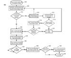
- FIG. 6 shows a flow diagram of task backpressure and drop determining process 600 of various destination processing modules of network processor 100 .
- a source processing module sends a task to a destination processing module.
- the destination processing module receives the task and determines the amount of cache memory (e.g., cache lines) required to store the PDU data corresponding to the task.
- destination processing module determines whether the used cache counter has reached a threshold. If the used cache counter has reached a threshold, at step 612 the destination processing module sends a backpressure message to the source module.
- Process 600 might return to step 604 to receive subsequent tasks.
- the destination processing module might optionally request an additional 2 KB memory block from the MMB at step 614 .
- the MMB grants the request for a new block (e.g., by providing an address of a new block)
- the destination processing module increments the queue depth counter by a number of cache lines in a memory block (e.g., by 8 if each cache line is 256 B and each memory block is 2 KB).
- the task depth counter has reached a threshold, then one or more tasks might be dropped at step 622 .
- step 616 if the MMB does not grant the request for a new block (e.g., no additional blocks are available), then at step 622 , the destination processing module drops one or more tasks. After tasks are dropped at step 622 , process 600 returns to step 604 to receive subsequent tasks. If, at step 620 , the task depth counter has not reached a threshold, then process 600 proceeds to step 624 . As shown in FIG. 6 , steps 614 , 616 , 618 , 620 and 622 might be performed optionally in some embodiments (as indicated by the dashed lines).
- destination processing module might determine whether to drop an incoming task might be based on a total size of PDU data in system memory 120 , or based on a total number of tasks in system memory 120 . If the number of tasks or the size of the PDU data in system memory 120 is below the minimum threshold, the new task is accepted. If the number of tasks or the size of the PDU data in system memory 120 is above the maximum threshold, the new task is dropped. If the number of tasks or the size of the PDU data in system memory 120 is between the minimum threshold and the maximum threshold, the drop probability of the new task might vary based on the drop probability profile where low priority tasks are dropped before high priority tasks are dropped.
- the destination processing module adds the received task to an associated queue of the destination processing module (e.g., based on task type, task priority, etc.).
- the destination processing module increments the used cache counter corresponding to the number of cache lines needed to store the received and accepted task.
- the destination processing module processes the tasks from the various queue(s).
- the destination processing module decrements the used queue counter and can delete, remove or otherwise invalidate the task data in the queue.
- process 600 completes.
- step 632 if removing the task data from the queue allows a memory block to become entirely unused, then at step 634 the destination module might release the memory block to the MMB and decrement the queue depth counter by the number of cache lines in the released memory block.
- step 638 process 600 completes.
- a source processing module sends a task message including a task identifier and a task size to a destination processing module.
- the destination module receives the task message and determines a task queue in which to store the task. Based on a used cache counter of the task queue and a number of cache lines required for the received task, the destination module determines whether the task queue has reached a usage threshold. If the task queue has reached the threshold, the destination module sends a backpressure message to the source module. Otherwise, if the task queue has not reached the threshold, the destination module accepts the received task, stores data of the received task in the task queue, increments the used cache counter for the task queue corresponding to the number of cache lines required for the received task, and processes the received task.
- described embodiments provide a packet classifier for a network processor that generates tasks corresponding to each received packet.
- the packet classifier includes a scheduler to generate contexts corresponding to tasks received by the packet classifier from a plurality of processing modules of the network processor.
- the packet classifier processes threads of instructions, each thread of instructions corresponding to a context received from the scheduler, and each thread associated with a data flow.
- a thread status table has N entries to track up to N active threads. Each status entry includes a valid status indicator, a sequence value, a thread indicator and a flow indicator.
- a sequence counter generates a sequence value for each data flow of each thread and is incremented when processing of a thread is started, and is decremented when a thread is completed. Instructions are processed in the order in which the threads were started for each data flow.
- Described embodiments might also be embodied in the form of methods and apparatuses for practicing those methods. Described embodiments might also be embodied in the form of program code embodied in tangible media, such as magnetic recording media, optical recording media, solid state memory, floppy diskettes, CD-ROMs, hard drives, or any other non-transitory machine-readable storage medium, wherein, when the program code is loaded into and executed by a machine, such as a computer, the machine becomes an apparatus for practicing the invention.
- Described embodiments might can also be embodied in the form of program code, for example, whether stored in a non-transitory machine-readable storage medium, loaded into and/or executed by a machine, or transmitted over some transmission medium or carrier, such as over electrical wiring or cabling, through fiber optics, or via electromagnetic radiation, wherein, when the program code is loaded into and executed by a machine, such as a computer, the machine becomes an apparatus for practicing the invention.
- program code segments combine with the processor to provide a unique device that operates analogously to specific logic circuits.
- Described embodiments might also be embodied in the form of a bitstream or other sequence of signal values electrically or optically transmitted through a medium, stored magnetic-field variations in a magnetic recording medium, etc., generated using a method and/or an apparatus of the present invention.
- the term “compatible” means that the element communicates with other elements in a manner wholly or partially specified by the standard, and would be recognized by other elements as sufficiently capable of communicating with the other elements in the manner specified by the standard.
- the compatible element does not need to operate internally in a manner specified by the standard.
- Couple refers to any manner known in the art or later developed in which energy is allowed to be transferred between two or more elements, and the interposition of one or more additional elements is contemplated, although not required.
- the terms “directly coupled,” “directly connected,” etc. imply the absence of such additional elements. Signals and corresponding nodes or ports might be referred to by the same name and are interchangeable for purposes here.
Abstract
Description
| TABLE 1 | ||
| USB | Universal Serial Bus | |
| SATA | Serial Advanced Technology Attachment | |
| SCSI | Small Computer System Interface | |
| SAS | Serial Attached SCSI | |
| PCI-E | Peripheral Component Interconnect Express | |
| SoC | System-on-Chip | |
| AXI | Advanced eXtensible Interface | |
| AMBA | Advanced Microcontroller Bus Architecture | |
| PAB | Packet Assembly Block | |
| MTM | Modular Traffic Manager | |
| DBC | Data Buffer Controller | |
| HE | Hash Engine | |
| SENG | State Engine | |
| TID | Task Identifier | |
| OUL | Oldest Unspecified List | |
| SCH | Scheduler | |
| SPP | Security Protocol Processor | |
| TIL | Task Input Logic | |
| TCP | Transmission Control Protocol | |
| IP | Internet Protocol | |
| FIFO | First-In, First-Out | |
| I/O | Input/Output | |
| DDR | Double Data Rate | |
| DRAM | Dynamic Random Access Memory | |
| MMB | Memory Manager Block | |
| μP | Microprocessor | |
| PLB | Processor Local Bus | |
| MPP | Modular Packet Processor | |
| AAL5 | ATM Adaptation Layer 5 | |
| SED | Stream Editor | |
| TID | Thread Identifier | |
| PQM | Pre-Queue Modifier | |
| FBI | Function Bus Interface | |
| CCL | Classification Completion List | |
| OC | Ordered Call | |
| SEM | Semaphore Engine | |
| PCM | Per Context Memory | |
| PDU | Protocol Data Unit | |
| PIC | Packet Integrity Checker | |
| CRC | Cyclic Redundancy Check | |
Claims (20)
Priority Applications (4)
| Application Number | Priority Date | Filing Date | Title |
|---|---|---|---|
| US13/687,958 US9461930B2 (en) | 2009-04-27 | 2012-11-28 | Modifying data streams without reordering in a multi-thread, multi-flow network processor |
| US13/687,865 US8910168B2 (en) | 2009-04-27 | 2012-11-28 | Task backpressure and deletion in a multi-flow network processor architecture |
| US13/705,822 US9727508B2 (en) | 2009-04-27 | 2012-12-05 | Address learning and aging for network bridging in a network processor |
| US13/756,849 US9444737B2 (en) | 2009-04-27 | 2013-02-01 | Packet data processor in a communications processor architecture |
Applications Claiming Priority (6)
| Application Number | Priority Date | Filing Date | Title |
|---|---|---|---|
| US12/430,438 US8352669B2 (en) | 2009-04-27 | 2009-04-27 | Buffered crossbar switch system |
| US12/782,411 US8407707B2 (en) | 2009-05-18 | 2010-05-18 | Task queuing in a network communications processor architecture |
| US12/782,379 US9081742B2 (en) | 2009-04-27 | 2010-05-18 | Network communications processor architecture |
| US12/782,393 US8255644B2 (en) | 2009-05-18 | 2010-05-18 | Network communications processor architecture with memory load balancing |
| US201161564811P | 2011-11-29 | 2011-11-29 | |
| US13/687,865 US8910168B2 (en) | 2009-04-27 | 2012-11-28 | Task backpressure and deletion in a multi-flow network processor architecture |
Related Parent Applications (1)
| Application Number | Title | Priority Date | Filing Date |
|---|---|---|---|
| US12/782,379 Continuation-In-Part US9081742B2 (en) | 2009-04-27 | 2010-05-18 | Network communications processor architecture |
Publications (2)
| Publication Number | Publication Date |
|---|---|
| US20130125127A1 US20130125127A1 (en) | 2013-05-16 |
| US8910168B2 true US8910168B2 (en) | 2014-12-09 |
Family
ID=48281941
Family Applications (1)
| Application Number | Title | Priority Date | Filing Date |
|---|---|---|---|
| US13/687,865 Expired - Fee Related US8910168B2 (en) | 2009-04-27 | 2012-11-28 | Task backpressure and deletion in a multi-flow network processor architecture |
Country Status (1)
| Country | Link |
|---|---|
| US (1) | US8910168B2 (en) |
Cited By (5)
| Publication number | Priority date | Publication date | Assignee | Title |
|---|---|---|---|---|
| US20150331710A1 (en) * | 2014-05-13 | 2015-11-19 | International Business Machines Corporation | Using queues corresponding to attribute values associated with units of work to select the units of work to process |
| US20150331716A1 (en) * | 2014-05-13 | 2015-11-19 | International Business Machines Corporation | Using queues corresponding to attribute values and priorities associated with units of work and sub-units of the unit of work to select the units of work and their sub-units to process |
| US20170019229A1 (en) * | 2015-07-17 | 2017-01-19 | Makoto Torikoshi | Communication apparatus, power control method, and recording medium |
| US9563366B2 (en) | 2014-05-13 | 2017-02-07 | International Business Machines Corporation | Using queues corresponding to attribute values associated with units of work and sub-units of the unit of work to select the units of work and their sub-units to process |
| US20230047454A1 (en) * | 2021-08-10 | 2023-02-16 | Mellanox Technologies, Ltd. | Ethernet pause aggregation for a relay device |
Families Citing this family (52)
| Publication number | Priority date | Publication date | Assignee | Title |
|---|---|---|---|---|
| US20110085443A1 (en) * | 2008-06-03 | 2011-04-14 | Hitachi. Ltd. | Packet Analysis Apparatus |
| WO2013100783A1 (en) | 2011-12-29 | 2013-07-04 | Intel Corporation | Method and system for control signalling in a data path module |
| WO2014096970A2 (en) * | 2012-12-20 | 2014-06-26 | Marvell World Trade Ltd. | Memory sharing in a network device |
| US9983801B1 (en) * | 2013-09-21 | 2018-05-29 | Avago Technologies General Ip (Singapore) Pte. Ltd. | Priority queueing for low latency storage networks |
| US10042768B1 (en) | 2013-09-21 | 2018-08-07 | Avago Technologies General Ip (Singapore) Pte. Ltd. | Virtual machine migration |
| US9547598B1 (en) * | 2013-09-21 | 2017-01-17 | Avego Technologies General Ip (Singapore) Pte. Ltd. | Cache prefill of cache memory for rapid start up of computer servers in computer networks |
| US10331583B2 (en) | 2013-09-26 | 2019-06-25 | Intel Corporation | Executing distributed memory operations using processing elements connected by distributed channels |
| US9207978B2 (en) * | 2013-10-09 | 2015-12-08 | Wipro Limited | Method and system for efficient execution of ordered and unordered tasks in multi-threaded and networked computing |
| CN104052676B (en) * | 2014-06-13 | 2017-12-05 | 华为技术有限公司 | A kind of data processing method of transmission path device and transmission path |
| US9742881B2 (en) * | 2014-06-30 | 2017-08-22 | Nicira, Inc. | Network virtualization using just-in-time distributed capability for classification encoding |
| US9965323B2 (en) * | 2015-03-11 | 2018-05-08 | Western Digital Technologies, Inc. | Task queues |
| GB2539445A (en) * | 2015-06-16 | 2016-12-21 | Nordic Semiconductor Asa | Data processing |
| US10067809B2 (en) * | 2016-04-20 | 2018-09-04 | International Business Machines Corporation | System and method for batch transport using hardware accelerators |
| US10970133B2 (en) | 2016-04-20 | 2021-04-06 | International Business Machines Corporation | System and method for hardware acceleration for operator parallelization with streams |
| US10558575B2 (en) * | 2016-12-30 | 2020-02-11 | Intel Corporation | Processors, methods, and systems with a configurable spatial accelerator |
| US10416999B2 (en) | 2016-12-30 | 2019-09-17 | Intel Corporation | Processors, methods, and systems with a configurable spatial accelerator |
| US10474375B2 (en) | 2016-12-30 | 2019-11-12 | Intel Corporation | Runtime address disambiguation in acceleration hardware |
| US10572376B2 (en) | 2016-12-30 | 2020-02-25 | Intel Corporation | Memory ordering in acceleration hardware |
| US10552326B2 (en) | 2017-05-23 | 2020-02-04 | International Business Machines Corporation | Reducing cache thrashing for counts in hot cache lines |
| US10515049B1 (en) | 2017-07-01 | 2019-12-24 | Intel Corporation | Memory circuits and methods for distributed memory hazard detection and error recovery |
| US10467183B2 (en) | 2017-07-01 | 2019-11-05 | Intel Corporation | Processors and methods for pipelined runtime services in a spatial array |
| US10515046B2 (en) | 2017-07-01 | 2019-12-24 | Intel Corporation | Processors, methods, and systems with a configurable spatial accelerator |
| US10445234B2 (en) | 2017-07-01 | 2019-10-15 | Intel Corporation | Processors, methods, and systems for a configurable spatial accelerator with transactional and replay features |
| US10469397B2 (en) | 2017-07-01 | 2019-11-05 | Intel Corporation | Processors and methods with configurable network-based dataflow operator circuits |
| US10445451B2 (en) | 2017-07-01 | 2019-10-15 | Intel Corporation | Processors, methods, and systems for a configurable spatial accelerator with performance, correctness, and power reduction features |
| US10387319B2 (en) | 2017-07-01 | 2019-08-20 | Intel Corporation | Processors, methods, and systems for a configurable spatial accelerator with memory system performance, power reduction, and atomics support features |
| US10496574B2 (en) | 2017-09-28 | 2019-12-03 | Intel Corporation | Processors, methods, and systems for a memory fence in a configurable spatial accelerator |
| US11086816B2 (en) | 2017-09-28 | 2021-08-10 | Intel Corporation | Processors, methods, and systems for debugging a configurable spatial accelerator |
| US10445098B2 (en) | 2017-09-30 | 2019-10-15 | Intel Corporation | Processors and methods for privileged configuration in a spatial array |
| US10380063B2 (en) | 2017-09-30 | 2019-08-13 | Intel Corporation | Processors, methods, and systems with a configurable spatial accelerator having a sequencer dataflow operator |
| US10740143B2 (en) * | 2017-10-06 | 2020-08-11 | International Business Machines Corporation | Controlling asynchronous tasks |
| US10417175B2 (en) | 2017-12-30 | 2019-09-17 | Intel Corporation | Apparatus, methods, and systems for memory consistency in a configurable spatial accelerator |
| US10445250B2 (en) | 2017-12-30 | 2019-10-15 | Intel Corporation | Apparatus, methods, and systems with a configurable spatial accelerator |
| US10565134B2 (en) | 2017-12-30 | 2020-02-18 | Intel Corporation | Apparatus, methods, and systems for multicast in a configurable spatial accelerator |
| US10564980B2 (en) | 2018-04-03 | 2020-02-18 | Intel Corporation | Apparatus, methods, and systems for conditional queues in a configurable spatial accelerator |
| US11307873B2 (en) | 2018-04-03 | 2022-04-19 | Intel Corporation | Apparatus, methods, and systems for unstructured data flow in a configurable spatial accelerator with predicate propagation and merging |
| US10810143B2 (en) * | 2018-04-03 | 2020-10-20 | Vmware, Inc. | Distributed storage system and method for managing storage access bandwidth for multiple clients |
| US10853073B2 (en) | 2018-06-30 | 2020-12-01 | Intel Corporation | Apparatuses, methods, and systems for conditional operations in a configurable spatial accelerator |
| US11200186B2 (en) | 2018-06-30 | 2021-12-14 | Intel Corporation | Apparatuses, methods, and systems for operations in a configurable spatial accelerator |
| US10459866B1 (en) | 2018-06-30 | 2019-10-29 | Intel Corporation | Apparatuses, methods, and systems for integrated control and data processing in a configurable spatial accelerator |
| US10891240B2 (en) | 2018-06-30 | 2021-01-12 | Intel Corporation | Apparatus, methods, and systems for low latency communication in a configurable spatial accelerator |
| US10678724B1 (en) | 2018-12-29 | 2020-06-09 | Intel Corporation | Apparatuses, methods, and systems for in-network storage in a configurable spatial accelerator |
| US10965602B2 (en) * | 2019-03-14 | 2021-03-30 | Intel Corporation | Software assisted hashing to improve distribution of a load balancer |
| US11029927B2 (en) | 2019-03-30 | 2021-06-08 | Intel Corporation | Methods and apparatus to detect and annotate backedges in a dataflow graph |
| US10915471B2 (en) | 2019-03-30 | 2021-02-09 | Intel Corporation | Apparatuses, methods, and systems for memory interface circuit allocation in a configurable spatial accelerator |
| US10817291B2 (en) | 2019-03-30 | 2020-10-27 | Intel Corporation | Apparatuses, methods, and systems for swizzle operations in a configurable spatial accelerator |
| US10965536B2 (en) | 2019-03-30 | 2021-03-30 | Intel Corporation | Methods and apparatus to insert buffers in a dataflow graph |
| US11037050B2 (en) | 2019-06-29 | 2021-06-15 | Intel Corporation | Apparatuses, methods, and systems for memory interface circuit arbitration in a configurable spatial accelerator |
| US11907713B2 (en) | 2019-12-28 | 2024-02-20 | Intel Corporation | Apparatuses, methods, and systems for fused operations using sign modification in a processing element of a configurable spatial accelerator |
| CN112596865A (en) * | 2020-12-22 | 2021-04-02 | 航天信息股份有限公司企业服务分公司 | System for pushing to-do message based on workflow affair |
| US11899601B1 (en) * | 2022-07-28 | 2024-02-13 | Beijing Tenafe Electronic Technology Co., Ltd. | Credit synchronization by sending a value for a local credit in a message sender from a message receiver to the message sender in response to a synchronization trigger |
| CN116483544B (en) * | 2023-06-15 | 2023-09-19 | 阿里健康科技(杭州)有限公司 | Task processing method, device, computer equipment and storage medium |
Citations (82)
| Publication number | Priority date | Publication date | Assignee | Title |
|---|---|---|---|---|
| US4123795A (en) | 1971-09-07 | 1978-10-31 | Texas Instruments Incorporated | Control system for a stored program multiprocessor computer |
| US4622631A (en) | 1983-12-30 | 1986-11-11 | Plexus Computers, Inc. | Data processing system having a data coherence solution |
| JPH02271444A (en) | 1989-04-13 | 1990-11-06 | Koufu Nippon Denki Kk | Address converting circuit |
| US5394534A (en) | 1992-09-11 | 1995-02-28 | International Business Machines Corporation | Data compression/decompression and storage of compressed and uncompressed data on a same removable data storage medium |
| US5623698A (en) | 1993-04-30 | 1997-04-22 | Cray Research, Inc. | Memory interconnect network having separate routing networks for inputs and outputs using switches with FIFO queues and message steering bits |
| US5838931A (en) | 1994-12-08 | 1998-11-17 | Intel Corporation | Method and apparatus for enabling a processor to access an external component through a private bus or a shared bus |
| US5892766A (en) | 1996-02-22 | 1999-04-06 | Fujitsu, Ltd. | Method and apparatus for coordinating access to an output of a routing device in a packet switching network |
| US5893120A (en) | 1997-01-02 | 1999-04-06 | Nemes; Richard Michael | Methods and apparatus for information storage and retrieval using a hashing technique with external chaining and on-the-fly removal of expired data |
| US5909695A (en) | 1995-10-13 | 1999-06-01 | Sun Microsystems, Inc. | Maximal concurrent lookup cache for computing systems having a multi-threaded environment |
| US5943283A (en) | 1997-12-05 | 1999-08-24 | Invox Technology | Address scrambling in a semiconductor memory |
| US5974421A (en) | 1996-12-23 | 1999-10-26 | Microsoft Corporation | Cache-efficient object loader |
| US6026467A (en) | 1997-10-01 | 2000-02-15 | Lucent Technologies Inc. | Content-addressable memory implemented with a memory management unit |
| US6038630A (en) | 1998-03-24 | 2000-03-14 | International Business Machines Corporation | Shared access control device for integrated system with multiple functional units accessing external structures over multiple data buses |
| US6052697A (en) | 1996-12-23 | 2000-04-18 | Microsoft Corporation | Reorganization of collisions in a hash bucket of a hash table to improve system performance |
| US6115802A (en) | 1995-10-13 | 2000-09-05 | Sun Mircrosystems, Inc. | Efficient hash table for use in multi-threaded environments |
| US6195335B1 (en) | 1997-06-27 | 2001-02-27 | International Business Machines Corporation | Data switch |
| US6216167B1 (en) | 1997-10-31 | 2001-04-10 | Nortel Networks Limited | Efficient path based forwarding and multicast forwarding |
| US6233246B1 (en) | 1996-12-30 | 2001-05-15 | Compaq Computer Corporation | Network switch with statistics read accesses |
| US6289013B1 (en) | 1998-02-09 | 2001-09-11 | Lucent Technologies, Inc. | Packet filter method and apparatus employing reduced memory |
| US6341130B1 (en) | 1998-02-09 | 2002-01-22 | Lucent Technologies, Inc. | Packet classification method and apparatus employing two fields |
| US20020029214A1 (en) | 2000-08-10 | 2002-03-07 | Nec Corporation | Synchronizable transactional database method and system |
| US20020165985A1 (en) | 2001-05-03 | 2002-11-07 | Jen-Kai Chen | Method for accessing a non-symmetric dual-slot address table and switching apparatus using same |
| US20030033276A1 (en) | 2001-08-09 | 2003-02-13 | Integrated Silicon Solution, Inc. | Search engine for large database search using CAM and hash |
| US6567564B1 (en) | 1996-04-17 | 2003-05-20 | Sarnoff Corporation | Pipelined pyramid processor for image processing systems |
| US20030115417A1 (en) | 2001-12-17 | 2003-06-19 | Corrigan Brian E. | Methods and apparatus for loading CRC values into a CRC cache in a storage controller |
| US6584546B2 (en) | 2001-01-16 | 2003-06-24 | Gautam Nag Kavipurapu | Highly efficient design of storage array for use in first and second cache spaces and memory subsystems |
| US20030123468A1 (en) | 2001-12-31 | 2003-07-03 | Stmicroelectronics, Inc. | Apparatus for switching data in high-speed networks and method of operation |
| US20030191857A1 (en) * | 2001-10-18 | 2003-10-09 | Terrell William C. | Router and methods using in-band link between managing processor and routing processor |
| US6636932B1 (en) | 1998-05-27 | 2003-10-21 | Micron Technology, Inc. | Crossbar switch and control for data networks switching |
| US6658012B1 (en) | 2000-04-27 | 2003-12-02 | International Business Machines Corporation | Statistics for VLAN bridging devices |
| US20040255209A1 (en) | 2003-06-10 | 2004-12-16 | Fred Gross | Apparatus and method for compressing redundancy information for embedded memories, including cache memories, of integrated circuits |
| US6839830B2 (en) | 2000-03-01 | 2005-01-04 | Realtek Semiconductor Corporation | Logical pipeline for data communications system |
| US20050027920A1 (en) | 2003-07-31 | 2005-02-03 | Fitzsimmons Michael D. | Crossbar switch that supports a multi-port slave device and method of operation |
| US6907469B1 (en) | 2000-04-11 | 2005-06-14 | International Business Machines Corporation | Method for bridging and routing data frames via a network switch comprising a special guided tree handler processor |
| US20050141537A1 (en) | 2003-12-29 | 2005-06-30 | Intel Corporation A Delaware Corporation | Auto-learning of MAC addresses and lexicographic lookup of hardware database |
| US6914882B2 (en) | 2001-03-30 | 2005-07-05 | Nokia, Inc. | Method and apparatus for improved queuing |
| US20050152352A1 (en) | 2003-12-27 | 2005-07-14 | Jong-Arm Jun | Scalable crossbar matrix switching apparatus and distributed scheduling method thereof |
| US20060029079A1 (en) | 2004-08-05 | 2006-02-09 | Cisco Technology, Inc. A California Corporation | Pipeline scheduler including a hierarchy of schedulers and multiple scheduling lanes |
| US7058057B2 (en) | 2001-05-01 | 2006-06-06 | Integrated Device Technology, Inc. | Network switch port traffic manager having configurable packet and cell servicing |
| US7085911B2 (en) | 2002-04-29 | 2006-08-01 | International Business Machines Corporation | Resizable cache sensitive hash table |
| US7089346B2 (en) | 2002-06-03 | 2006-08-08 | International Business Machines Corporation | Method of operating a crossbar switch |
| US20060256783A1 (en) | 2005-04-06 | 2006-11-16 | Robert Ayrapetian | Buffered crossbar switch with a linear buffer to port relationship that supports cells and packets of variable size |
| US7159219B2 (en) | 2001-12-21 | 2007-01-02 | Agere Systems Inc. | Method and apparatus for providing multiple data class differentiation with priorities using a single scheduling structure |
| US20070011396A1 (en) | 2005-06-30 | 2007-01-11 | Utstarcom, Inc. | Method and apparatus for bandwidth efficient and bounded latency packet buffering |
| US20070016756A1 (en) | 2005-07-15 | 2007-01-18 | Jen-Wei Hsieh | Device for identifying data characteristics for flash memory |
| US20070043856A1 (en) | 2005-02-07 | 2007-02-22 | Metavize, Inc. | Methods and systems for low-latency event pipelining |
| US7234018B1 (en) | 2001-07-11 | 2007-06-19 | Pasternak Solutions Llc | Layered crossbar for interconnection of multiple processors and shared memories |
| US20070226798A1 (en) | 1999-07-29 | 2007-09-27 | Intertrust Technologies Corporation | Systems and methods for using cryptography to protect secure and insecure computing environments |
| US7287046B2 (en) | 2002-09-30 | 2007-10-23 | Emc Corporation | Method and system of compacting sparse directories in a file system |
| US20070271374A1 (en) | 2006-05-18 | 2007-11-22 | Alaxala Networks Corporation | Statistical information collecting system and apparatus thereof |
| US20080077928A1 (en) | 2006-09-27 | 2008-03-27 | Kabushiki Kaisha Toshiba | Multiprocessor system |
| US20080092092A1 (en) | 2004-10-04 | 2008-04-17 | Damian Jude Dalton | Method and Processor for Power Analysis in Digital Circuits |
| US20080162793A1 (en) | 2006-12-28 | 2008-07-03 | Genesys Logic, Inc. | Management method for reducing utilization rate of random access memory (ram) used in flash memory |
| US7397809B2 (en) | 2002-12-13 | 2008-07-08 | Conexant Systems, Inc. | Scheduling methods for combined unicast and multicast queuing |
| US20080240103A1 (en) | 2007-03-30 | 2008-10-02 | Andreas Schmidt | Three-port ethernet switch with external buffer |
| US20080240106A1 (en) | 2007-03-30 | 2008-10-02 | Ralph Schlenk | Method and apparatus for MAC address learning |
| US20080239992A1 (en) | 2007-03-26 | 2008-10-02 | Qualcomm Incorporated | Methods and apparatus for performing channel tree operations |
| US7453898B1 (en) | 2002-03-30 | 2008-11-18 | Cisco Technology, Inc. | Methods and apparatus for simultaneously scheduling multiple priorities of packets |
| US7461407B2 (en) | 2004-02-05 | 2008-12-02 | Research In Motion Limited | Debugging port security interface |
| US7461208B1 (en) | 2005-06-16 | 2008-12-02 | Sun Microsystems, Inc. | Circuitry and method for accessing an associative cache with parallel determination of data and data availability |
| US20090019270A1 (en) | 2007-07-13 | 2009-01-15 | Digi International Inc. | Embedded device program debug control |
| US7512740B2 (en) | 2003-05-30 | 2009-03-31 | Mips Technologies, Inc. | Microprocessor with improved data stream prefetching |
| US7519065B2 (en) | 1999-05-14 | 2009-04-14 | Nortel Networks Limited | Multicast and unicast scheduling for a network device |
| US7554464B1 (en) | 2004-09-30 | 2009-06-30 | Gear Six, Inc. | Method and system for processing data having a pattern of repeating bits |
| US7594028B1 (en) | 2000-04-28 | 2009-09-22 | International Business Machines Corporation | Counting of GVRP protocol data units within a network bridge |
| US7596142B1 (en) | 2006-05-12 | 2009-09-29 | Integrated Device Technology, Inc | Packet processing in a packet switch with improved output data distribution |
| US7600078B1 (en) | 2006-03-29 | 2009-10-06 | Intel Corporation | Speculatively performing read transactions |
| US20090271562A1 (en) | 2008-04-25 | 2009-10-29 | Sinclair Alan W | Method and system for storage address re-mapping for a multi-bank memory device |
| US7660259B1 (en) | 2004-10-20 | 2010-02-09 | Extreme Networks, Inc. | Methods and systems for hybrid hardware- and software-base media access control (MAC) address learning |
| US7659894B2 (en) | 2000-06-19 | 2010-02-09 | Mental Images Gmbh | Terminating spatial partition hierarchies by a priori bounding memory |
| US7710988B1 (en) | 2005-03-11 | 2010-05-04 | Xambala Corporation | Method and system for non-deterministic finite automaton filtering |
| US7720055B2 (en) | 1999-03-17 | 2010-05-18 | Broadcom Corporation | Method for handling IP multicast packets in network switch |
| US20100260198A1 (en) | 2009-04-08 | 2010-10-14 | Roberto Rojas-Cessa | Space-Space-Memory (SSM) Clos-Network Packet Switch |
| US7849315B2 (en) | 2006-05-22 | 2010-12-07 | General Dynamics C4 Systems, Inc. | Method for managing operability of on-chip debug capability |
| US7886150B2 (en) | 2007-05-11 | 2011-02-08 | Mips Technologies, Inc. | System debug and trace system and method, and applications thereof |
| US20110219195A1 (en) | 2010-03-02 | 2011-09-08 | Adi Habusha | Pre-fetching of data packets |
| US20120023498A1 (en) * | 2010-05-18 | 2012-01-26 | Lsi Corporation | Local messaging in a scheduling hierarchy in a traffic manager of a network processor |
| US20120020368A1 (en) * | 2009-04-27 | 2012-01-26 | Lsi Corporation | Dynamic updating of scheduling hierarchy in a traffic manager of a network processor |
| US20120023295A1 (en) * | 2010-05-18 | 2012-01-26 | Lsi Corporation | Hybrid address mutex mechanism for memory accesses in a network processor |
| US20120020370A1 (en) * | 2010-05-18 | 2012-01-26 | Lsi Corporation | Root scheduling algorithm in a network processor |
| US8127350B2 (en) | 2010-06-30 | 2012-02-28 | Juniper Networks, Inc. | Multi-service VPN network client for mobile device |
| US8140759B2 (en) | 2009-04-16 | 2012-03-20 | International Business Machines Corporation | Specifying an access hint for prefetching partial cache block data in a cache hierarchy |
-
2012
- 2012-11-28 US US13/687,865 patent/US8910168B2/en not_active Expired - Fee Related
Patent Citations (83)
| Publication number | Priority date | Publication date | Assignee | Title |
|---|---|---|---|---|
| US4123795A (en) | 1971-09-07 | 1978-10-31 | Texas Instruments Incorporated | Control system for a stored program multiprocessor computer |
| US4622631A (en) | 1983-12-30 | 1986-11-11 | Plexus Computers, Inc. | Data processing system having a data coherence solution |
| US4622631B1 (en) | 1983-12-30 | 1996-04-09 | Recognition Int Inc | Data processing system having a data coherence solution |
| JPH02271444A (en) | 1989-04-13 | 1990-11-06 | Koufu Nippon Denki Kk | Address converting circuit |
| US5394534A (en) | 1992-09-11 | 1995-02-28 | International Business Machines Corporation | Data compression/decompression and storage of compressed and uncompressed data on a same removable data storage medium |
| US5623698A (en) | 1993-04-30 | 1997-04-22 | Cray Research, Inc. | Memory interconnect network having separate routing networks for inputs and outputs using switches with FIFO queues and message steering bits |
| US5838931A (en) | 1994-12-08 | 1998-11-17 | Intel Corporation | Method and apparatus for enabling a processor to access an external component through a private bus or a shared bus |
| US5909695A (en) | 1995-10-13 | 1999-06-01 | Sun Microsystems, Inc. | Maximal concurrent lookup cache for computing systems having a multi-threaded environment |
| US6115802A (en) | 1995-10-13 | 2000-09-05 | Sun Mircrosystems, Inc. | Efficient hash table for use in multi-threaded environments |
| US5892766A (en) | 1996-02-22 | 1999-04-06 | Fujitsu, Ltd. | Method and apparatus for coordinating access to an output of a routing device in a packet switching network |
| US6567564B1 (en) | 1996-04-17 | 2003-05-20 | Sarnoff Corporation | Pipelined pyramid processor for image processing systems |
| US5974421A (en) | 1996-12-23 | 1999-10-26 | Microsoft Corporation | Cache-efficient object loader |
| US6052697A (en) | 1996-12-23 | 2000-04-18 | Microsoft Corporation | Reorganization of collisions in a hash bucket of a hash table to improve system performance |
| US6233246B1 (en) | 1996-12-30 | 2001-05-15 | Compaq Computer Corporation | Network switch with statistics read accesses |
| US5893120A (en) | 1997-01-02 | 1999-04-06 | Nemes; Richard Michael | Methods and apparatus for information storage and retrieval using a hashing technique with external chaining and on-the-fly removal of expired data |
| US6195335B1 (en) | 1997-06-27 | 2001-02-27 | International Business Machines Corporation | Data switch |
| US6026467A (en) | 1997-10-01 | 2000-02-15 | Lucent Technologies Inc. | Content-addressable memory implemented with a memory management unit |
| US6216167B1 (en) | 1997-10-31 | 2001-04-10 | Nortel Networks Limited | Efficient path based forwarding and multicast forwarding |
| US5943283A (en) | 1997-12-05 | 1999-08-24 | Invox Technology | Address scrambling in a semiconductor memory |
| US6289013B1 (en) | 1998-02-09 | 2001-09-11 | Lucent Technologies, Inc. | Packet filter method and apparatus employing reduced memory |
| US6341130B1 (en) | 1998-02-09 | 2002-01-22 | Lucent Technologies, Inc. | Packet classification method and apparatus employing two fields |
| US6038630A (en) | 1998-03-24 | 2000-03-14 | International Business Machines Corporation | Shared access control device for integrated system with multiple functional units accessing external structures over multiple data buses |
| US6636932B1 (en) | 1998-05-27 | 2003-10-21 | Micron Technology, Inc. | Crossbar switch and control for data networks switching |
| US7720055B2 (en) | 1999-03-17 | 2010-05-18 | Broadcom Corporation | Method for handling IP multicast packets in network switch |
| US7519065B2 (en) | 1999-05-14 | 2009-04-14 | Nortel Networks Limited | Multicast and unicast scheduling for a network device |
| US20070226798A1 (en) | 1999-07-29 | 2007-09-27 | Intertrust Technologies Corporation | Systems and methods for using cryptography to protect secure and insecure computing environments |
| US6839830B2 (en) | 2000-03-01 | 2005-01-04 | Realtek Semiconductor Corporation | Logical pipeline for data communications system |
| US6907469B1 (en) | 2000-04-11 | 2005-06-14 | International Business Machines Corporation | Method for bridging and routing data frames via a network switch comprising a special guided tree handler processor |
| US6658012B1 (en) | 2000-04-27 | 2003-12-02 | International Business Machines Corporation | Statistics for VLAN bridging devices |
| US7594028B1 (en) | 2000-04-28 | 2009-09-22 | International Business Machines Corporation | Counting of GVRP protocol data units within a network bridge |
| US7659894B2 (en) | 2000-06-19 | 2010-02-09 | Mental Images Gmbh | Terminating spatial partition hierarchies by a priori bounding memory |
| US20020029214A1 (en) | 2000-08-10 | 2002-03-07 | Nec Corporation | Synchronizable transactional database method and system |
| US6584546B2 (en) | 2001-01-16 | 2003-06-24 | Gautam Nag Kavipurapu | Highly efficient design of storage array for use in first and second cache spaces and memory subsystems |
| US6914882B2 (en) | 2001-03-30 | 2005-07-05 | Nokia, Inc. | Method and apparatus for improved queuing |
| US7058057B2 (en) | 2001-05-01 | 2006-06-06 | Integrated Device Technology, Inc. | Network switch port traffic manager having configurable packet and cell servicing |
| US20020165985A1 (en) | 2001-05-03 | 2002-11-07 | Jen-Kai Chen | Method for accessing a non-symmetric dual-slot address table and switching apparatus using same |
| US7234018B1 (en) | 2001-07-11 | 2007-06-19 | Pasternak Solutions Llc | Layered crossbar for interconnection of multiple processors and shared memories |
| US20030033276A1 (en) | 2001-08-09 | 2003-02-13 | Integrated Silicon Solution, Inc. | Search engine for large database search using CAM and hash |
| US20030191857A1 (en) * | 2001-10-18 | 2003-10-09 | Terrell William C. | Router and methods using in-band link between managing processor and routing processor |
| US20030115417A1 (en) | 2001-12-17 | 2003-06-19 | Corrigan Brian E. | Methods and apparatus for loading CRC values into a CRC cache in a storage controller |
| US7159219B2 (en) | 2001-12-21 | 2007-01-02 | Agere Systems Inc. | Method and apparatus for providing multiple data class differentiation with priorities using a single scheduling structure |
| US20030123468A1 (en) | 2001-12-31 | 2003-07-03 | Stmicroelectronics, Inc. | Apparatus for switching data in high-speed networks and method of operation |
| US7453898B1 (en) | 2002-03-30 | 2008-11-18 | Cisco Technology, Inc. | Methods and apparatus for simultaneously scheduling multiple priorities of packets |
| US7085911B2 (en) | 2002-04-29 | 2006-08-01 | International Business Machines Corporation | Resizable cache sensitive hash table |
| US7089346B2 (en) | 2002-06-03 | 2006-08-08 | International Business Machines Corporation | Method of operating a crossbar switch |
| US7287046B2 (en) | 2002-09-30 | 2007-10-23 | Emc Corporation | Method and system of compacting sparse directories in a file system |
| US7397809B2 (en) | 2002-12-13 | 2008-07-08 | Conexant Systems, Inc. | Scheduling methods for combined unicast and multicast queuing |
| US7512740B2 (en) | 2003-05-30 | 2009-03-31 | Mips Technologies, Inc. | Microprocessor with improved data stream prefetching |
| US20040255209A1 (en) | 2003-06-10 | 2004-12-16 | Fred Gross | Apparatus and method for compressing redundancy information for embedded memories, including cache memories, of integrated circuits |
| US20050027920A1 (en) | 2003-07-31 | 2005-02-03 | Fitzsimmons Michael D. | Crossbar switch that supports a multi-port slave device and method of operation |
| US20050152352A1 (en) | 2003-12-27 | 2005-07-14 | Jong-Arm Jun | Scalable crossbar matrix switching apparatus and distributed scheduling method thereof |
| US20050141537A1 (en) | 2003-12-29 | 2005-06-30 | Intel Corporation A Delaware Corporation | Auto-learning of MAC addresses and lexicographic lookup of hardware database |
| US7461407B2 (en) | 2004-02-05 | 2008-12-02 | Research In Motion Limited | Debugging port security interface |
| US20060029079A1 (en) | 2004-08-05 | 2006-02-09 | Cisco Technology, Inc. A California Corporation | Pipeline scheduler including a hierarchy of schedulers and multiple scheduling lanes |
| US7554464B1 (en) | 2004-09-30 | 2009-06-30 | Gear Six, Inc. | Method and system for processing data having a pattern of repeating bits |
| US20080092092A1 (en) | 2004-10-04 | 2008-04-17 | Damian Jude Dalton | Method and Processor for Power Analysis in Digital Circuits |
| US7660259B1 (en) | 2004-10-20 | 2010-02-09 | Extreme Networks, Inc. | Methods and systems for hybrid hardware- and software-base media access control (MAC) address learning |
| US20070043856A1 (en) | 2005-02-07 | 2007-02-22 | Metavize, Inc. | Methods and systems for low-latency event pipelining |
| US7710988B1 (en) | 2005-03-11 | 2010-05-04 | Xambala Corporation | Method and system for non-deterministic finite automaton filtering |
| US20060256783A1 (en) | 2005-04-06 | 2006-11-16 | Robert Ayrapetian | Buffered crossbar switch with a linear buffer to port relationship that supports cells and packets of variable size |
| US7461208B1 (en) | 2005-06-16 | 2008-12-02 | Sun Microsystems, Inc. | Circuitry and method for accessing an associative cache with parallel determination of data and data availability |
| US20070011396A1 (en) | 2005-06-30 | 2007-01-11 | Utstarcom, Inc. | Method and apparatus for bandwidth efficient and bounded latency packet buffering |
| US20070016756A1 (en) | 2005-07-15 | 2007-01-18 | Jen-Wei Hsieh | Device for identifying data characteristics for flash memory |
| US7600078B1 (en) | 2006-03-29 | 2009-10-06 | Intel Corporation | Speculatively performing read transactions |
| US7596142B1 (en) | 2006-05-12 | 2009-09-29 | Integrated Device Technology, Inc | Packet processing in a packet switch with improved output data distribution |
| US20070271374A1 (en) | 2006-05-18 | 2007-11-22 | Alaxala Networks Corporation | Statistical information collecting system and apparatus thereof |
| US7849315B2 (en) | 2006-05-22 | 2010-12-07 | General Dynamics C4 Systems, Inc. | Method for managing operability of on-chip debug capability |
| US20080077928A1 (en) | 2006-09-27 | 2008-03-27 | Kabushiki Kaisha Toshiba | Multiprocessor system |
| US20080162793A1 (en) | 2006-12-28 | 2008-07-03 | Genesys Logic, Inc. | Management method for reducing utilization rate of random access memory (ram) used in flash memory |
| US20080239992A1 (en) | 2007-03-26 | 2008-10-02 | Qualcomm Incorporated | Methods and apparatus for performing channel tree operations |
| US20080240103A1 (en) | 2007-03-30 | 2008-10-02 | Andreas Schmidt | Three-port ethernet switch with external buffer |
| US20080240106A1 (en) | 2007-03-30 | 2008-10-02 | Ralph Schlenk | Method and apparatus for MAC address learning |
| US7886150B2 (en) | 2007-05-11 | 2011-02-08 | Mips Technologies, Inc. | System debug and trace system and method, and applications thereof |
| US20090019270A1 (en) | 2007-07-13 | 2009-01-15 | Digi International Inc. | Embedded device program debug control |
| US20090271562A1 (en) | 2008-04-25 | 2009-10-29 | Sinclair Alan W | Method and system for storage address re-mapping for a multi-bank memory device |
| US20100260198A1 (en) | 2009-04-08 | 2010-10-14 | Roberto Rojas-Cessa | Space-Space-Memory (SSM) Clos-Network Packet Switch |
| US8140759B2 (en) | 2009-04-16 | 2012-03-20 | International Business Machines Corporation | Specifying an access hint for prefetching partial cache block data in a cache hierarchy |
| US20120020368A1 (en) * | 2009-04-27 | 2012-01-26 | Lsi Corporation | Dynamic updating of scheduling hierarchy in a traffic manager of a network processor |
| US20110219195A1 (en) | 2010-03-02 | 2011-09-08 | Adi Habusha | Pre-fetching of data packets |
| US20120023498A1 (en) * | 2010-05-18 | 2012-01-26 | Lsi Corporation | Local messaging in a scheduling hierarchy in a traffic manager of a network processor |
| US20120023295A1 (en) * | 2010-05-18 | 2012-01-26 | Lsi Corporation | Hybrid address mutex mechanism for memory accesses in a network processor |
| US20120020370A1 (en) * | 2010-05-18 | 2012-01-26 | Lsi Corporation | Root scheduling algorithm in a network processor |
| US8127350B2 (en) | 2010-06-30 | 2012-02-28 | Juniper Networks, Inc. | Multi-service VPN network client for mobile device |
Non-Patent Citations (5)
| Title |
|---|
| Alan H. Karp and Rajiv Gupta, "Hardware Assist for Data Merging for Shared Memory Multiprocessors", Hewlett-Packard Labs, Palo Alto, CA, Mar. 13, 1994. |
| Chiueh et al., "High-Performance IP Routing Table Lookup Using CPU Caching", IEEE (1999). |
| Lu, Sheng, Dinda. "Size-based Scheduling Policies with Inaccurate Scheduling Information", Proceedings of the IEEE Computer Society's 12th Annual International Symposium on Modeling, Analysis, and Simulation of Computer and Telecommunications Systems (2004). |
| Schurgers, Raghunathan, Srivastava. "Modulation Scaling for Real-time Energy Aware Packet Scheduling", IEEE, Nov. 2001. |
| Sundaram, Chandra, Goyal, Shenoy, Sahni, Vin. "Application Performance in the QLinux Multimedia Operating System", ACM Multimedia, Los Angeles, CA (2000). |
Cited By (9)
| Publication number | Priority date | Publication date | Assignee | Title |
|---|---|---|---|---|
| US20150331710A1 (en) * | 2014-05-13 | 2015-11-19 | International Business Machines Corporation | Using queues corresponding to attribute values associated with units of work to select the units of work to process |
| US20150331716A1 (en) * | 2014-05-13 | 2015-11-19 | International Business Machines Corporation | Using queues corresponding to attribute values and priorities associated with units of work and sub-units of the unit of work to select the units of work and their sub-units to process |
| US9563366B2 (en) | 2014-05-13 | 2017-02-07 | International Business Machines Corporation | Using queues corresponding to attribute values associated with units of work and sub-units of the unit of work to select the units of work and their sub-units to process |
| US9575800B2 (en) * | 2014-05-13 | 2017-02-21 | International Business Machines Corporation | Using queues corresponding to attribute values and priorities associated with units of work and sub-units of the unit of work to select the units of work and their sub-units to process |
| US9921879B2 (en) * | 2014-05-13 | 2018-03-20 | International Business Machines Corporation | Using queues corresponding to attribute values associated with units of work to select the units of work to process |
| US20170019229A1 (en) * | 2015-07-17 | 2017-01-19 | Makoto Torikoshi | Communication apparatus, power control method, and recording medium |
| US10051562B2 (en) * | 2015-07-17 | 2018-08-14 | Ricoh Company, Ltd. | Communication apparatus, power control method, and recording medium |
| US20230047454A1 (en) * | 2021-08-10 | 2023-02-16 | Mellanox Technologies, Ltd. | Ethernet pause aggregation for a relay device |
| US11888753B2 (en) * | 2021-08-10 | 2024-01-30 | Mellanox Technologies, Ltd. | Ethernet pause aggregation for a relay device |
Also Published As
| Publication number | Publication date |
|---|---|
| US20130125127A1 (en) | 2013-05-16 |
Similar Documents
| Publication | Publication Date | Title |
|---|---|---|
| US8910168B2 (en) | Task backpressure and deletion in a multi-flow network processor architecture | |
| US8761204B2 (en) | Packet assembly module for multi-core, multi-thread network processors | |
| US8499137B2 (en) | Memory manager for a network communications processor architecture | |
| US8917738B2 (en) | Multicasting traffic manager in a network communications processor architecture | |
| US9183145B2 (en) | Data caching in a network communications processor architecture | |
| US9218290B2 (en) | Data caching in a network communications processor architecture | |
| US8515965B2 (en) | Concurrent linked-list traversal for real-time hash processing in multi-core, multi-thread network processors | |
| US10552205B2 (en) | Work conserving, load balancing, and scheduling | |
| US8873550B2 (en) | Task queuing in a multi-flow network processor architecture | |
| US8407707B2 (en) | Task queuing in a network communications processor architecture | |
| US9461930B2 (en) | Modifying data streams without reordering in a multi-thread, multi-flow network processor | |
| US8539199B2 (en) | Hash processing in a network communications processor architecture | |
| US8321385B2 (en) | Hash processing in a network communications processor architecture | |
| US8949838B2 (en) | Multi-threaded processing with hardware accelerators | |
| US9444757B2 (en) | Dynamic configuration of processing modules in a network communications processor architecture | |
| US8677075B2 (en) | Memory manager for a network communications processor architecture | |
| US8949582B2 (en) | Changing a flow identifier of a packet in a multi-thread, multi-flow network processor | |
| US9444737B2 (en) | Packet data processor in a communications processor architecture | |
| US9152564B2 (en) | Early cache eviction in a multi-flow network processor architecture | |
| US20110225372A1 (en) | Concurrent, coherent cache access for multiple threads in a multi-core, multi-thread network processor | |
| US8683221B2 (en) | Configurable memory encryption with constant pipeline delay in a multi-core processor | |
| US8943507B2 (en) | Packet assembly module for multi-core, multi-thread network processors | |
| US8874878B2 (en) | Thread synchronization in a multi-thread, multi-flow network communications processor architecture |
Legal Events
| Date | Code | Title | Description |
|---|---|---|---|
| AS | Assignment |
Owner name: LSI CORPORATION, CALIFORNIA Free format text: ASSIGNMENT OF ASSIGNORS INTEREST;ASSIGNORS:MITAL, DEEPAK;BURROUGHS, WILLIAM;BETKER, MICHAEL R.;REEL/FRAME:029367/0268 Effective date: 20121128 |
|
| AS | Assignment |
Owner name: DEUTSCHE BANK AG NEW YORK BRANCH, AS COLLATERAL AG Free format text: PATENT SECURITY AGREEMENT;ASSIGNORS:LSI CORPORATION;AGERE SYSTEMS LLC;REEL/FRAME:032856/0031 Effective date: 20140506 |
|
| AS | Assignment |
Owner name: LSI CORPORATION, CALIFORNIA Free format text: TERMINATION AND RELEASE OF SECURITY INTEREST IN PATENTS AT REEL/FRAME NO. 32856/0031;ASSIGNOR:DEUTSCHE BANK AG NEW YORK BRANCH;REEL/FRAME:034286/0872 Effective date: 20141118 Owner name: AGERE SYSTEMS LLC, PENNSYLVANIA Free format text: TERMINATION AND RELEASE OF SECURITY INTEREST IN PATENTS AT REEL/FRAME NO. 32856/0031;ASSIGNOR:DEUTSCHE BANK AG NEW YORK BRANCH;REEL/FRAME:034286/0872 Effective date: 20141118 |
|
| FEPP | Fee payment procedure |
Free format text: PAYOR NUMBER ASSIGNED (ORIGINAL EVENT CODE: ASPN); ENTITY STATUS OF PATENT OWNER: LARGE ENTITY |
|
| AS | Assignment |
Owner name: INTEL CORPORATION, CALIFORNIA Free format text: ASSIGNMENT OF ASSIGNORS INTEREST;ASSIGNOR:LSI CORPORATION;REEL/FRAME:035090/0477 Effective date: 20141114 |
|
| AS | Assignment |
Owner name: AGERE SYSTEMS LLC, PENNSYLVANIA Free format text: TERMINATION AND RELEASE OF SECURITY INTEREST IN PATENT RIGHTS (RELEASES RF 032856-0031);ASSIGNOR:DEUTSCHE BANK AG NEW YORK BRANCH, AS COLLATERAL AGENT;REEL/FRAME:037684/0039 Effective date: 20160201 Owner name: LSI CORPORATION, CALIFORNIA Free format text: TERMINATION AND RELEASE OF SECURITY INTEREST IN PATENT RIGHTS (RELEASES RF 032856-0031);ASSIGNOR:DEUTSCHE BANK AG NEW YORK BRANCH, AS COLLATERAL AGENT;REEL/FRAME:037684/0039 Effective date: 20160201 |
|
| FEPP | Fee payment procedure |
Free format text: MAINTENANCE FEE REMINDER MAILED (ORIGINAL EVENT CODE: REM.) |
|
| LAPS | Lapse for failure to pay maintenance fees |
Free format text: PATENT EXPIRED FOR FAILURE TO PAY MAINTENANCE FEES (ORIGINAL EVENT CODE: EXP.); ENTITY STATUS OF PATENT OWNER: LARGE ENTITY |
|
| STCH | Information on status: patent discontinuation |
Free format text: PATENT EXPIRED DUE TO NONPAYMENT OF MAINTENANCE FEES UNDER 37 CFR 1.362 |
|
| FP | Lapsed due to failure to pay maintenance fee |
Effective date: 20181209 |