US8074082B2 - Anti-tamper module - Google Patents
Anti-tamper module Download PDFInfo
- Publication number
- US8074082B2 US8074082B2 US11/248,659 US24865905A US8074082B2 US 8074082 B2 US8074082 B2 US 8074082B2 US 24865905 A US24865905 A US 24865905A US 8074082 B2 US8074082 B2 US 8074082B2
- Authority
- US
- United States
- Prior art keywords
- tamper module
- integrated circuit
- logic device
- configurable logic
- memory
- Prior art date
- Legal status (The legal status is an assumption and is not a legal conclusion. Google has not performed a legal analysis and makes no representation as to the accuracy of the status listed.)
- Active, expires
Links
Images


Classifications
-
- H—ELECTRICITY
- H01—ELECTRIC ELEMENTS
- H01L—SEMICONDUCTOR DEVICES NOT COVERED BY CLASS H10
- H01L23/00—Details of semiconductor or other solid state devices
- H01L23/57—Protection from inspection, reverse engineering or tampering
- H01L23/576—Protection from inspection, reverse engineering or tampering using active circuits
-
- G—PHYSICS
- G06—COMPUTING; CALCULATING OR COUNTING
- G06F—ELECTRIC DIGITAL DATA PROCESSING
- G06F21/00—Security arrangements for protecting computers, components thereof, programs or data against unauthorised activity
- G06F21/70—Protecting specific internal or peripheral components, in which the protection of a component leads to protection of the entire computer
- G06F21/86—Secure or tamper-resistant housings
- G06F21/87—Secure or tamper-resistant housings by means of encapsulation, e.g. for integrated circuits
-
- H—ELECTRICITY
- H01—ELECTRIC ELEMENTS
- H01L—SEMICONDUCTOR DEVICES NOT COVERED BY CLASS H10
- H01L23/00—Details of semiconductor or other solid state devices
- H01L23/48—Arrangements for conducting electric current to or from the solid state body in operation, e.g. leads, terminal arrangements ; Selection of materials therefor
- H01L23/488—Arrangements for conducting electric current to or from the solid state body in operation, e.g. leads, terminal arrangements ; Selection of materials therefor consisting of soldered or bonded constructions
- H01L23/498—Leads, i.e. metallisations or lead-frames on insulating substrates, e.g. chip carriers
- H01L23/49811—Additional leads joined to the metallisation on the insulating substrate, e.g. pins, bumps, wires, flat leads
- H01L23/49816—Spherical bumps on the substrate for external connection, e.g. ball grid arrays [BGA]
-
- H—ELECTRICITY
- H01—ELECTRIC ELEMENTS
- H01L—SEMICONDUCTOR DEVICES NOT COVERED BY CLASS H10
- H01L25/00—Assemblies consisting of a plurality of individual semiconductor or other solid state devices ; Multistep manufacturing processes thereof
- H01L25/03—Assemblies consisting of a plurality of individual semiconductor or other solid state devices ; Multistep manufacturing processes thereof all the devices being of a type provided for in the same subgroup of groups H01L27/00 - H01L33/00, or in a single subclass of H10K, H10N, e.g. assemblies of rectifier diodes
- H01L25/04—Assemblies consisting of a plurality of individual semiconductor or other solid state devices ; Multistep manufacturing processes thereof all the devices being of a type provided for in the same subgroup of groups H01L27/00 - H01L33/00, or in a single subclass of H10K, H10N, e.g. assemblies of rectifier diodes the devices not having separate containers
- H01L25/065—Assemblies consisting of a plurality of individual semiconductor or other solid state devices ; Multistep manufacturing processes thereof all the devices being of a type provided for in the same subgroup of groups H01L27/00 - H01L33/00, or in a single subclass of H10K, H10N, e.g. assemblies of rectifier diodes the devices not having separate containers the devices being of a type provided for in group H01L27/00
- H01L25/0657—Stacked arrangements of devices
-
- H—ELECTRICITY
- H01—ELECTRIC ELEMENTS
- H01L—SEMICONDUCTOR DEVICES NOT COVERED BY CLASS H10
- H01L2223/00—Details relating to semiconductor or other solid state devices covered by the group H01L23/00
- H01L2223/58—Structural electrical arrangements for semiconductor devices not otherwise provided for
- H01L2223/64—Impedance arrangements
- H01L2223/66—High-frequency adaptations
- H01L2223/6661—High-frequency adaptations for passive devices
- H01L2223/6677—High-frequency adaptations for passive devices for antenna, e.g. antenna included within housing of semiconductor device
-
- H—ELECTRICITY
- H01—ELECTRIC ELEMENTS
- H01L—SEMICONDUCTOR DEVICES NOT COVERED BY CLASS H10
- H01L2224/00—Indexing scheme for arrangements for connecting or disconnecting semiconductor or solid-state bodies and methods related thereto as covered by H01L24/00
- H01L2224/01—Means for bonding being attached to, or being formed on, the surface to be connected, e.g. chip-to-package, die-attach, "first-level" interconnects; Manufacturing methods related thereto
- H01L2224/10—Bump connectors; Manufacturing methods related thereto
- H01L2224/15—Structure, shape, material or disposition of the bump connectors after the connecting process
- H01L2224/16—Structure, shape, material or disposition of the bump connectors after the connecting process of an individual bump connector
-
- H—ELECTRICITY
- H01—ELECTRIC ELEMENTS
- H01L—SEMICONDUCTOR DEVICES NOT COVERED BY CLASS H10
- H01L2225/00—Details relating to assemblies covered by the group H01L25/00 but not provided for in its subgroups
- H01L2225/03—All the devices being of a type provided for in the same subgroup of groups H01L27/00 - H01L33/648 and H10K99/00
- H01L2225/04—All the devices being of a type provided for in the same subgroup of groups H01L27/00 - H01L33/648 and H10K99/00 the devices not having separate containers
- H01L2225/065—All the devices being of a type provided for in the same subgroup of groups H01L27/00 - H01L33/648 and H10K99/00 the devices not having separate containers the devices being of a type provided for in group H01L27/00
- H01L2225/06503—Stacked arrangements of devices
- H01L2225/06548—Conductive via connections through the substrate, container, or encapsulation
-
- H—ELECTRICITY
- H01—ELECTRIC ELEMENTS
- H01L—SEMICONDUCTOR DEVICES NOT COVERED BY CLASS H10
- H01L2225/00—Details relating to assemblies covered by the group H01L25/00 but not provided for in its subgroups
- H01L2225/03—All the devices being of a type provided for in the same subgroup of groups H01L27/00 - H01L33/648 and H10K99/00
- H01L2225/04—All the devices being of a type provided for in the same subgroup of groups H01L27/00 - H01L33/648 and H10K99/00 the devices not having separate containers
- H01L2225/065—All the devices being of a type provided for in the same subgroup of groups H01L27/00 - H01L33/648 and H10K99/00 the devices not having separate containers the devices being of a type provided for in group H01L27/00
- H01L2225/06503—Stacked arrangements of devices
- H01L2225/06551—Conductive connections on the side of the device
-
- H—ELECTRICITY
- H01—ELECTRIC ELEMENTS
- H01L—SEMICONDUCTOR DEVICES NOT COVERED BY CLASS H10
- H01L2225/00—Details relating to assemblies covered by the group H01L25/00 but not provided for in its subgroups
- H01L2225/03—All the devices being of a type provided for in the same subgroup of groups H01L27/00 - H01L33/648 and H10K99/00
- H01L2225/04—All the devices being of a type provided for in the same subgroup of groups H01L27/00 - H01L33/648 and H10K99/00 the devices not having separate containers
- H01L2225/065—All the devices being of a type provided for in the same subgroup of groups H01L27/00 - H01L33/648 and H10K99/00 the devices not having separate containers the devices being of a type provided for in group H01L27/00
- H01L2225/06503—Stacked arrangements of devices
- H01L2225/06555—Geometry of the stack, e.g. form of the devices, geometry to facilitate stacking
- H01L2225/06565—Geometry of the stack, e.g. form of the devices, geometry to facilitate stacking the devices having the same size and there being no auxiliary carrier between the devices
-
- H—ELECTRICITY
- H01—ELECTRIC ELEMENTS
- H01L—SEMICONDUCTOR DEVICES NOT COVERED BY CLASS H10
- H01L27/00—Devices consisting of a plurality of semiconductor or other solid-state components formed in or on a common substrate
- H01L27/02—Devices consisting of a plurality of semiconductor or other solid-state components formed in or on a common substrate including semiconductor components specially adapted for rectifying, oscillating, amplifying or switching and having at least one potential-jump barrier or surface barrier; including integrated passive circuit elements with at least one potential-jump barrier or surface barrier
-
- H—ELECTRICITY
- H01—ELECTRIC ELEMENTS
- H01L—SEMICONDUCTOR DEVICES NOT COVERED BY CLASS H10
- H01L2924/00—Indexing scheme for arrangements or methods for connecting or disconnecting semiconductor or solid-state bodies as covered by H01L24/00
- H01L2924/0001—Technical content checked by a classifier
- H01L2924/00011—Not relevant to the scope of the group, the symbol of which is combined with the symbol of this group
-
- H—ELECTRICITY
- H01—ELECTRIC ELEMENTS
- H01L—SEMICONDUCTOR DEVICES NOT COVERED BY CLASS H10
- H01L2924/00—Indexing scheme for arrangements or methods for connecting or disconnecting semiconductor or solid-state bodies as covered by H01L24/00
- H01L2924/0001—Technical content checked by a classifier
- H01L2924/00014—Technical content checked by a classifier the subject-matter covered by the group, the symbol of which is combined with the symbol of this group, being disclosed without further technical details
-
- H—ELECTRICITY
- H01—ELECTRIC ELEMENTS
- H01L—SEMICONDUCTOR DEVICES NOT COVERED BY CLASS H10
- H01L2924/00—Indexing scheme for arrangements or methods for connecting or disconnecting semiconductor or solid-state bodies as covered by H01L24/00
- H01L2924/15—Details of package parts other than the semiconductor or other solid state devices to be connected
- H01L2924/151—Die mounting substrate
- H01L2924/153—Connection portion
- H01L2924/1531—Connection portion the connection portion being formed only on the surface of the substrate opposite to the die mounting surface
- H01L2924/15311—Connection portion the connection portion being formed only on the surface of the substrate opposite to the die mounting surface being a ball array, e.g. BGA
Definitions
- the present invention concerns the protection of devices from tampering and, in particular, concerns a module having multiple anti-tamper mechanisms incorporated therein.
- Custom made devices are often the most difficult to analyze.
- increasing demands to reduce both development time and overall costs have led to an increased reliance on off-the-shelf components to implement devices.
- the use of off-the-shelf components gives an opponent a head start at examining the device since the features and functionality of the individual components are easily obtained.
- conventional techniques for arranging the components within a device often facilitate visual identification of both the individual components and many of the connections between the components.
- the present invention addresses the foregoing needs by providing a generic platform for protecting the features and functionality of one or more components using multiple anti-tamper mechanisms.
- Significant innovations of the invention can be categorized into three general anti-tamper mechanisms.
- the first mechanism is the use of a stacking architecture to assemble the anti-tamper module.
- the second mechanism is the rerouting of connections within the module.
- the third mechanism is the incorporation of code in the module for controlling access to the components. This code is generally referred to as a key.
- the invention uses different combinations and variations of these three mechanisms, as well as others described in the detailed description, to provide an innovative anti-tamper module.
- an anti-tamper module for protecting the contents of an integrated circuit.
- the anti-tamper module includes a connection layer having an input/output connector for connecting the module to an external system.
- a memory connected to the connection layer stores code for controlling access to the contents of the integrated circuit, which also is connected to the connection layer.
- the components of the anti-tamper module are arranged in a stacked configuration.
- an anti-tamper module for protecting the contents of an integrated circuit.
- the anti-tamper module includes a connection layer having input/output connectors for connecting the anti-tamper module to an external system.
- the integrated circuit also includes input/output connectors.
- a configurable logic device is connected to both the connection layer and the integrated circuit.
- the configurable logic device is configured to create logical circuits connecting at least one of the input/output connectors of the connection layer to at least one of the input/output connectors of the integrated circuit.
- the anti-tamper module further includes a memory storing code for controlling access to the contents of the integrated circuit.
- the components of the anti-tamper module are arranged in a stacked configuration.
- FIG. 1 is a diagram depicting the generic components of an anti-tamper platform provided by the invention.
- FIGS. 2A , 2 B and 2 C are diagrams depicting three primary configurations of an anti-tamper module according to three embodiments of the invention.
- FIG. 3 is a cross-section of two components depicting two examples of interconnecting techniques used to form an anti-tamper module according to one embodiment of the invention.
- FIGS. 4A and 4B are diagrams depicting the arrangements of input/output connectors on components witin an anti-tamper module according to one embodiment of the invention.
- FIG. 5 is a diagram depicting the logical rerouting of connections between components in an anti-tamper module according to one embodiment of the invention.
- FIG. 6 is a diagram depicting the components of an anti-tamper module according to one embodiment of the invention.
- FIG. 7 is a diagram depicting the components of an anti-tamper module according to one embodiment of the invention.
- FIG. 8 is a diagram depicting the components of an anti-tamper module according to one embodiment of the invention.
- FIG. 9 is a diagram depicting the components of an anti-tamper module according to one embodiment of the invention.
- FIG. 10 is a diagram depicting an anti-tamper module encased in a protective layer according to one embodiment of the invention.
- FIG. 1 is a diagram depicting the generalized layers of an anti-tamper module 10 according to one embodiment of the invention.
- Anti-tamper module 10 includes a protected layer 11 , an active layer 12 and a connection layer 13 .
- Protected layer 11 represents one or more integrated circuits protected within anti-tamper module 10 .
- Possible integrated circuits include, but are not limited to, random access memory (RAM), processors, application-specific integrated circuits (ASIC), etc.
- RAM random access memory
- ASIC application-specific integrated circuits
- the contents of an integrated circuit refer to any code and/or data stored within the integrated circuit as well as the structure and functionality of the integrated circuit itself.
- Active layer 12 represents hardware components used to provide one or more anti-tamper mechanisms. These anti-tamper mechanisms are used to inhibit the unauthorized probing and reverse engineering of an integrated circuit incorporated within the module.
- These hardware components include memory, both volatile and non-volatile, and configurable logic devices such as field programmable gate arrays (FPGA) and field programmable interconnect devices (FPID). The operation of the hardware components and their associated anti-tamper mechanisms will be described in more detail below.
- Connection layer 13 represents the input/output connection used to connect anti-tamper module 10 to an external system that uses the one or more integrated circuits within protected layer 11 for operation.
- Connection layer 13 includes one or more connectors used to electrically communicate signals between the external system and anti-tamper module 10 .
- the connectors may be balls within a ball grid array (BGA), pins, or other types of connectors known to those skilled in the art.
- connection layer 13 may implement a known interface standard, such as the Peripheral Component Interconnect (PCI) standard, for communication between the external system and anti-tamper module 10 .
- PCI Peripheral Component Interconnect
- FIG. 1 shows a single protected layer 11 and a single active layer 12 . It is to be understood that the invention is not limited to this arrangement. As will be appreciated by one skilled in the art, the anti-tamper module may include multiple protected layers 11 and/or multiple active layers 12 .
- FIGS. 2A , 2 B and 2 C depict three general configurations of the invention.
- FIG. 2A depicts the configuration of anti-tamper module 20 a according to one embodiment of the invention.
- Anti-tamper module 20 a includes integrated circuit (IC) 21 , memory 22 and connection layer 23 .
- IC 21 represents one or more integrated circuits whose contents are protected by anti-tamper module 20 a .
- Memory 22 represents a memory which stores code for controlling access to the contents of IC 21 .
- Connection layer 23 connects anti-tamper module 20 a to an external system (not shown) using connectors 24 .
- Connectors 24 represent balls in a BGA, pins or other connectors known to those skilled in the art.
- FIG. 2B depicts the configuration of anti-tamper module 20 b according to another embodiment of the invention.
- anti-tamper module 20 b includes IC 21 , connection layer 23 and connectors 24 .
- configurable logic device 25 is also included in anti-tamper module 20 b , which is configurable to create logical circuits connecting at least one input/output connector of IC 21 to at least one connector 24 of connection layer 23 .
- FIG. 2C depicts the configuration of anti-tamper module 20 c according to another embodiment of the invention.
- Anti-tamper module 20 c includes IC 21 , connection layer 23 and connectors 24 . Additionally, anti-tamper module 20 c includes memory 22 , as in anti-tamper module 20 a , and configurable logic device 23 , as in anti-tamper module 20 b.
- the invention is not limited to the embodiments depicted in FIGS. 2A , 2 B and 2 C.
- Alternative embodiments of the invention may include multiple ICs 21 , memories 22 and/or configurable logic devices 25 .
- the order in which the components of the anti-tamper module are stacked may be varied in different embodiments. The functions and anti-tamper mechanisms provided by these components will be described in more detail below.
- the components of the anti-tamper modules are arranged in a stacked configuration.
- the components are stacked and interconnected using any of a number of stacking techniques known to those skilled in the art. For example, Irvine Sensors Corporation has developed several patented techniques for stacking and interconnecting multiple integrated circuits. Some of these techniques are set forth in U.S. Pat. Nos.
- components containing integrated circuits are bonded together one on top of another so as to maintain a footprint equivalent to that of a single component.
- the input/output connections of the individual components are routed to the edges of the components. This routing may be due to component packaging, such as thin small-outline packaging, or may be done using interposers positioned between the components to accommodate other types of component packaging.
- Interposers typically are printed circuit boards connected to a component using a BGA or some other type of connection mechanism. Conductive traces formed on the interposer route the input/output connections of the component to the edges of the interposer.
- FIG. 3 is a cross section of two components showing two examples of interconnection techniques. As depicted in FIG. 3 , component 30 a is stacked and bonded on top of component 30 b . Component 30 a includes integrated circuit 31 a encapsulated in packaging material 32 a . Similarly, component 30 b includes integrated circuit 31 b encapsulated in packaging material 32 b . Input/output connectors 33 a and 34 a extend through packaging material 32 a to the edges of component 30 a . Likewise, input/output connectors 33 b and 34 b extend through packaging material 32 b to the edges of component 30 b.
- FIG. 3 One technique exemplified in FIG. 3 is the use of a conductive trace or wire 35 to interconnect input/output connectors 34 a and 34 b .
- Metal trace or wire 35 is formed on the edge of the component stack to interconnect the two components.
- Another technique exemplified in FIG. 3 is the use of metallization and vias to interconnect components.
- conductive trace or wire 36 a extends from input/output connector 33 a and a conductive trace or wire 36 b extends from input/output connector 33 b .
- These two conductive traces or wires are interconnected with metal filled within via 37 formed through filing materials 38 a and 38 b .
- a variety of materials known to those skilled in the art can be used for packing materials 32 a and 32 b and filing materials 38 a and 38 b.
- vias such as via 37 provides certain advantages over the use of a conductive wire or trace formed on the edge of the component stack. For example, the use of vias both hides and protects the interconnections between components with the stack. However, different embodiments of the invention may use either of these techniques by themselves, or a combination of these techniques to interconnect components. In addition, it is noted that FIG. 3 only depicts one interconnection on each side of the stack. One skilled in the art will recognize that the present invention contemplates several such interconnections on one or more sides of the component stack of an anti-tamper module arranged according to different embodiments of the invention.
- the routing and interconnection of input/output connectors within the anti-tamper module provide an anti-tamper mechanism by allowing the input/output connectors accessible to an external system to be scrambled.
- the input/output connectors of the components stacked in the anti-tamper module are routed to the edges of the stack and then interconnected. This allows the arrangement of the input/output connectors of one component connected to the connection layer to be different than the arrangement of the input/output connectors of the connection layer itself.
- FIGS. 4A and 4B depict a simple example of this rearrangement.
- FIG. 4A includes a component 40 a having six input/output connectors A, B, C, D, E and F.
- Component 40 a represents a protected integrated circuit within an anti-tamper module or some other component within the stack.
- FIG. 4B includes connection layer 40 b having six input/output connectors for connecting to an external system.
- the input/output connectors shown in FIG. 4B are labeled to indicate connections to the six input/output connectors A, B, C, D, E and F of component 40 a in FIG. 4A . Comparing FIGS.
- connection layer 40 b demonstrates a simple example of modifying the arrangement of the input/output connectors of component 40 a as accessible by an external system through connection layer 40 b . If the proper arrangement of the input/output connectors on connection layer 40 b is unknown to an unauthorized user, the ability to correctly access and use component 40 a in an anti-tamper module is greatly reduced.
- configurable logic device 25 is used to logically re-route connections between components within an anti-tamper module.
- configurable logic device 25 represents a reconfigurable device, such as a field programmable gate array or a field programmable interconnect device, that is capable of being configured to form logical circuits connecting different input/output connectors.
- the logical circuits are created using configuration information such as code in a hardware description language that is loaded into configurable logic device 25 . This code may be loaded at the time of manufacture or first use to permanently configure the logical circuits, thereby hardwiring configurable logic device 25 .
- the code may be loaded when the anti-tamper device is connected to an external system via connection layer 23 and is provided power to execute configuration processes.
- Another alternative is to store the code in memory 22 or in a portion of configurable logic device 25 configured as memory, and load the code from this location rather than from an external system.
- the general structure and techniques for programming FPGAs and FPIDs are known to those skilled in the art and will not be discussed further in this description.
- the logical circuits within configurable logic device 25 are disconnected when the anti-tamper module is disconnected from power. Accordingly, when the anti-tamper module is removed from a system, connections within the module that are necessary for operation cannot be probed through connection layer 23 . Instead, probing the anti-tamper module when removed from a system leads to dead-end connections sometimes referred to as cul-de-sacs.
- FIG. 5 is a block diagram depicting the re-routing of connections between components within anti-tamper module 50 according to one embodiment of the invention.
- logical circuit 51 is formed between connectors A and B of configurable logic device 25 .
- Logical circuit 51 routes the connection between connector AA of integrated circuit 21 and connector BB of connectors 24 through configurable logic device 25 .
- the connection is routed from connector AA to the edge of the module through interposer 52 .
- Conductor 53 routes the connection down the side of the component stack to connection layer 23 .
- Connection layer 23 routes the connection to connector A and routes the connection from connect B to connector BB of connectors 24 .
- logical circuit 54 is formed between connectors C and D of configurable logic device 25 .
- Logical circuit 54 routes the connection between connectors CC and DD of memory 22 through configurable logic device 25 .
- the connection is routed from connector CC to the edge of the module through interposer 55 .
- Conductor 56 routes the connection down the side of the component stack to connection layer 23 .
- Connection layer 23 routes the connection to connector C and routes the connection from connector D back to the edge of the component stack.
- Conductor 57 routes the connection up the side of the component stack to interposer 55 , which routes the connection to connector DD of memory 22 .
- logical circuit 54 is shown as being open thereby leaving connectors CC and DD disconnected.
- FIG. 5 depicts two connections re-routed through configurable logic device 25 , with one of the connections configured to connect one of the components to an external system through connection layer 23 and the other connection configured to remain within anti-tamper module 50 . It is to be understood, however, that more than one of each of these types of configurable connections can and preferably are used to re-route connections within anti-tamper module 50 .
- the input/output connectors 24 are not necessarily in a one-to-one correspondence with the internal connections of the module. Additionally, other physical connections between components will be hidden within the component stack. In this manner, the invention makes it more difficult to determine the contents of the module by probing input/output connectors 24 . Additionally, the functional arrangement of the input/output connectors 24 can be scrambled using different configurations within configurable logic device 25 .
- one or more keys are incorporated in an anti-tamper module as an additional anti-tamper mechanism.
- keys are generally defined as code used to control access to the contents of integrated circuits in the protected layer of an anti-tamper module.
- Keys useful in the present invention include passwords or data patterns used to authorize access to integrated circuit 21 , executable code used to perform algorithms necessary to access the contents of integrated circuit 21 , cryptographic keys used for data encryption/decryption, encryption/decryption algorithms for encrypting/decrypting data, etc.
- the invention is not limited to specific types of the keys mentioned above and can include many types and variations known to those skilled in art. For example, the lengths and complexities of the keys may vary.
- a number of encryption algorithms such as those based on the Advanced Encryption Standard, may be used.
- the significant aspects of the keys in the invention involve how the keys are incorporated into the anti-tamper module. Multiple levels of security can be established by incorporating different types and numbers of keys in the anti-tamper module. Depending on the application and the environment the anti-tamper module is to be used in, an appropriate level of security can be selected and implemented in the module.
- a first level of security uses a software key that is stored on a computing device separate from the anti-tamper module.
- the software key is loaded into the anti-tamper module.
- the software key is stored in memory 22 .
- the software key can be stored in a portion of configurable logic device 25 that has been configured as memory. This type of key can be used with an Access Control List to provide multiple levels of access to the module. This type of key also can be modified during operation of the anti-tamper module.
- a second level of security uses a software key that is stored within the anti-tamper module.
- the software key may be stored in memory 22 of an anti-tamper module such as those depicted in FIGS. 2A and 2C .
- the software key may be stored in a portion of configurable logic device 25 configured as a memory in anti-tamper modules such as those depicted in FIGS. 2B and 2C .
- the key may be programmed into configurable logic device 25 .
- configuration information is loaded into configurable logic device 25 to program a software key therein. By modifying the configuration information, the software key is reconfigurable and can vary in length and type.
- One example of the second level key described above is a password or encryption key necessary to access the contents of integrated circuit 21 in the anti-tamper module depicted in FIG. 2A .
- a password or encryption key is stored in memory 22 .
- the external system When anti-tamper module 20 a is connected to an external system, the external system must access a specific portion of memory 22 to retrieve the password or encryption key in order to access integrated circuit 21 . Without the password or encryption key, access to integrated circuit will be prohibited, or at a minimum will produce a useless output.
- an unauthorized user of the anti-tamper module will be impeded in attempts to access the contents of integrated circuit 21 by requiring the user to be aware of the need to retrieve the password or encryption key, requiring knowledge of where the password or encryption key is stored and how to access it, and requiring knowledge of how the password or encryption key is used to control access.
- the present invention provides a generic platform for protecting the contents of an integrated circuit.
- the stacked architecture used to assemble the anti-tamper module gives this platform the ability to add functionality to the anti-tamper module by incorporating additional layers into the component stack.
- this generic platform is represented by protected layer 11 , active layer 12 and connection layer 13 , similar to the layers described in FIG. 1 .
- Each of FIGS. 6 to 9 generally depicts the addition of functional layers to the anti-tamper module to provide additional functionality and improved anti-tamper mechanisms.
- connection layer 13 being located at the base of the anti-tamper module, the order of the arrangement of components can vary in different embodiments of the invention.
- a third level of key security uses a firmware or hard key that is embedded within the component stack.
- a key is represented by key 61 incorporated into the component stack of anti-tamper module 60 shown in FIG. 6 .
- the hard key is a physical electronic key implemented in a chip that is included in the stack of components at the time of manufacturing anti-tamper module 60 .
- the hard key is fixed at the time of manufacture and is not reconfigurable.
- the presence of hard key 61 is difficult to detect within the component stack. Even if the presence of hard key 61 is known, an understanding of how the hard key functions and is integrated with the other components in the stack is necessary to be able to reverse engineer the module to gain access to the contents of protected layer 11 .
- the anti-tamper module can be configured to utilize hard key 61 embedded in the component stack, two soft keys programmed into a configurable logic device within active layer 12 , and a soft key received via a connected external system.
- hard key 61 embedded in the component stack two soft keys programmed into a configurable logic device within active layer 12
- a soft key received via a connected external system can be implemented in the invention.
- One skilled in the art will recognize other combinations of capable of use within the anti-tamper module without departing from the scope of the invention.
- FIG. 7 is a diagram depicting anti-tamper module 70 according to one embodiment of the invention.
- anti-tamper module 70 includes an internal power source 71 incorporated within the component stack.
- power source 71 is a battery having a life cycle sufficient for the particular application the anti-tamper module is to be used for.
- Power source 71 can be a rechargeable battery capable of recharging itself when the anti-tamper module is connected to an external system providing power to the module.
- the battery may be arranged within the component stack to have no connections to an external system through connection layer 13 , thereby making detection of the battery difficult.
- Power source 71 provides power to anti-tamper module 70 , thereby allowing one or more operations or functions to be executed within anti-tamper module 70 regardless of whether the module is connected to and receiving power from an external system. Exemplary operations and functions are described below.
- the anti-tamper module is configured to remove traces of certain functionality within the module. This functionality includes, but is not limited to, the logical circuits programmed in the configurable logic device, software keys programmed in the configurable logic device, software keys stored in the memory, and configuration information for programming the configurable logic device stored within the anti-tamper module.
- any configurable logic device that is not hardwired is lost. In this state, the configurable logic device is no longer able to provide the previously programmed functionality.
- sophisticated probing and/or imaging techniques may be able to recover the previous states of the electronic components within the configurable logic device. Using the recovered states, the operating configuration of the configurable logic device could possibly be recreated thereby allowing unauthorized access to the contents of the protected integrated circuit.
- code containing a series of read/write commands is executed to place the electronic components in a default state such as a zero state. Code containing a similar series of read/write commands also can be executed to place the electronic components of the memory in a default state, thereby erasing any code, keys or data stored therein. This process is referred to as zeroization.
- the reset or zeroization code is stored within the anti-tamper module.
- a non-active portion of the configurable logic device may be set aside for storing the zeroization code. Storing the code in a non-active portion of the device helps ensure that the code is not unintentionally accessed and executed.
- the zeroization code may be stored in a non-volatile section of the memory.
- the zeroization code is executed by a processor within the anti-tamper module.
- the configurable logic device such as an FPGA, may be configured to include one or more processors for this purpose. Alternatively, a separate processor may be incorporated as a layer within the component stack of the anti-tamper module.
- processors capable of performing these functions.
- the zeroization code is executed in response to a trigger event.
- the trigger event may be a command or code received by the anti-tamper module, or it can be a detected condition or state of the module.
- power source 71 is used to provide sufficient power to execute the zeroization code.
- power source 71 In addition to providing power to execute operations or functions with the anti-tamper module, power source 71 also can provide internal power for other uses. For example, power source 71 may provide power to maintain data storage in volatile memory within the component stack of the anti-tamper module. Referring back to FIG. 2A , if memory 22 is implemented using volatile memory, power must be maintained to memory 22 in order to retain the code stored therein. Power source 71 can provide this power for the useful life of the anti-tamper module.
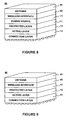
- wireless functionality is added to anti-tamper module 80 depicted in FIG. 8 .
- wireless functionality is added by incorporating antenna 81 and wireless interface 82 into the component stack.
- power source 71 also is included within the component stack.
- Antenna 81 and wireless interface 82 allow anti-tamper module 80 to send and receive data using any of a number of wireless protocols. For example, heavily encrypted spread-spectrum wireless protocols may be used to securely transmit and/or receive data.
- Antenna 81 and wireless interface 82 may be used to receive a radio frequency encryption key which is then stored in a memory within active layer 12 to protect access to the contents of an integrated circuit within protected layer 11 .
- antenna 81 and wireless interface 82 may receive unique code as a signal that the zeroization code described above be executed within the anti-tamper module. Accordingly, a trigger event may occur when the anti-tamper module receives the unique code.
- Antenna 81 can be implemented using any of a number of designs known to those skilled in the art.
- antenna 81 is formed by depositing metal on a substrate and shaping the metal into the desired antenna configuration.
- An antenna formed in this manner allows the presence of the antenna within the anti-tamper module to be less noticeable and possibly hidden from inspection of the anti-tamper module.
- Wireless interface 82 includes the necessary circuitry to receive a radio signal via antenna 81 , decode the radio signal, convert the signal into digital format for use by other components within the anti-tamper module.
- Typical receivers, converters, processors, controllers, etc. used to implement wireless interface 82 are generally known and will not be described further herein. Any of a number of designs and configurations known to those skilled in the art can be used for antenna 81 and wireless interface 82 .
- FIG. 9 depicts anti-tamper module 90 having antenna 81 and wireless interface 82 incorporated within the component stack.
- anti-tamper module 90 does not include power source 71 .
- an alternative to power source 71 is provided by using inductive coupling with antenna 81 .
- Wireless interface 82 is configured to include circuitry to capture this current and distribute power internally to other components within anti-tamper module 90 .
- This type of power source is commonly used today in radio frequency ID tags and tollway transponders.
- anti-tamper module 90 can be provided with power to perform specific operations and functions such as the execution of the zeroization code discussed above.
- the functional features mentioned above with reference to FIGS. 6 to 9 have been described as being incorporated individually into the anti-tamper module. It is to be understood, that any combination of these functional features can be implemented within a single anti-tamper module without departing from the scope of the invention. It is further noted that the functionality of the anti-tamper module is scalable. For example, multiple instances of the functional layers described with reference to FIG. 6 to 9 can be incorporated into the component stack and additional configurable logic devices, memory modules, and/or integrated circuits also can be incorporated into the component stack to increase the functionality of the module.
- the anti-tamper module is typically encased in a protective layer.
- the protective layer is a passive protection device that impedes inspection of the anti-tamper module.
- anti-tamper module 100 is encased by protective layer 101 .
- only connectors 24 extend through the protective layer to allow the anti-tamper module to be connected to an external system.
- Other components of the anti-tamper module may not be encased by protective layer 101 in other embodiments of the invention.
- the first level of protection offered by protective layer 101 is impeding visual inspection of the anti-tamper module.
- protective layer 101 includes an opaque material, such as an epoxy or a metal, that prevents visual inspection of the individual components within anti-tamper module 100 as well as any interconnects formed on the side of the component stack. In this manner, the anti-tamper module appears as a single component rather than a stack of multiple components, thereby making discernment of the configuration of the module more difficult.
- Protective layer 101 also protects the components of the anti-tamper module from physical damage and tampering by sealing the components inside.
- the materials of protective layer 101 can be selected to impede other forms of inspection such as x-ray scanning.
- the contents and arrangement of the anti-tamper module can be obscured from x-ray scanning and other sophisticated scanning technologies.
- a wire mesh encased in epoxy might be used to form the protective layer. While the epoxy prevents visual inspection, the wire mesh disguises the contents of the anti-tamper module from discernment using x-ray scanning.
- Other combinations of materials having desirable properties and benefits may be used in the protective layer without departing from the scope of the invention.
- protective layer 101 describes a passive anti-tamper mechanism provided by encasing the anti-tamper module with protective layer 101 .
- Protective layer 101 can also be arranged to provide an active layer of protection. For example, using electrically conducting materials within the protective layer allows electrical circuits to be formed throughout the protective layer. Physical intrusion through the protective layer will break one or more of these electrical circuits causing an open circuit. Using a detector connected to the electrical circuits allows intrusion to be detected and appropriate action taken. Such action may include simply shutting down operation of the anti-tamper module. Additionally, detected intrusion may be used as a trigger event to initiate the execute of the reset or zeroization code described above.
- U.S. Pat. Nos. 5,539,379 and 5,858,500 which are assigned to W.L. Gore & Associates, Inc., and are incorporated herein by reference, describe protective enclosures that may be used within the context of the present invention.
- Other embodiments of the invention may use one or more ground planes arranged as protective plates on one or more sides or ends of the anti-tamper module. These ground planes are typically made of a material such as copper. In addition to acting as a ground plane, the protective plates inhibit the ability to inspect and/or scan the contents of the anti-tamper module.
- the present invention provides an anti-tamper module that uses multiple anti-tamper mechanisms to protect the contents of one or more integrated circuits incorporated within the module.
- the design and arrangement of the anti-tamper module described above does not require custom components and can be assembled using off-the-shelf components. This simplifies the design process and shortens the time required to produce anti-tamper modules.
Abstract
Description
Claims (63)
Priority Applications (1)
| Application Number | Priority Date | Filing Date | Title |
|---|---|---|---|
| US11/248,659 US8074082B2 (en) | 2004-10-08 | 2005-10-11 | Anti-tamper module |
Applications Claiming Priority (2)
| Application Number | Priority Date | Filing Date | Title |
|---|---|---|---|
| US61735604P | 2004-10-08 | 2004-10-08 | |
| US11/248,659 US8074082B2 (en) | 2004-10-08 | 2005-10-11 | Anti-tamper module |
Publications (2)
| Publication Number | Publication Date |
|---|---|
| US20060087883A1 US20060087883A1 (en) | 2006-04-27 |
| US8074082B2 true US8074082B2 (en) | 2011-12-06 |
Family
ID=36206020
Family Applications (1)
| Application Number | Title | Priority Date | Filing Date |
|---|---|---|---|
| US11/248,659 Active 2028-07-14 US8074082B2 (en) | 2004-10-08 | 2005-10-11 | Anti-tamper module |
Country Status (1)
| Country | Link |
|---|---|
| US (1) | US8074082B2 (en) |
Cited By (5)
| Publication number | Priority date | Publication date | Assignee | Title |
|---|---|---|---|---|
| US20120185636A1 (en) * | 2010-08-04 | 2012-07-19 | Isc8, Inc. | Tamper-Resistant Memory Device With Variable Data Transmission Rate |
| US20140136852A1 (en) * | 2012-11-09 | 2014-05-15 | Crossbar, Inc. | Secure circuit integrated with memory layer |
| US8938627B2 (en) * | 2009-07-07 | 2015-01-20 | International Business Machines Corporation | Multilayer securing structure and method thereof for the protection of cryptographic keys and code |
| US20180262353A1 (en) * | 2017-03-07 | 2018-09-13 | Nxp B.V. | Method and apparatus for binding stacked die using a physically unclonable function |
| US11329010B2 (en) | 2019-04-11 | 2022-05-10 | Cryptography Research, Inc. | Integrated circuit shield |
Families Citing this family (31)
| Publication number | Priority date | Publication date | Assignee | Title |
|---|---|---|---|---|
| US7535373B2 (en) * | 2005-07-15 | 2009-05-19 | Honeywell International, Inc. | Security techniques for electronic devices |
| US7429926B1 (en) * | 2005-07-20 | 2008-09-30 | Xilinx, Inc. | Radio frequency identification (RFID) and programmable logic device (PLD) integration and applications |
| US7495554B2 (en) * | 2006-01-11 | 2009-02-24 | Honeywell International Inc. | Clamshell protective encasement |
| US7792302B2 (en) * | 2006-02-01 | 2010-09-07 | Dolby Laboratories Licensing Corporation | Securely coupling an FPGA to a security IC |
| US7479798B1 (en) | 2006-05-16 | 2009-01-20 | Altera Corporation | Selectively disabled output |
| US7710286B1 (en) | 2007-03-30 | 2010-05-04 | Maxim Integrated Products, Inc. | Intrusion detection using a conductive material |
| US7923830B2 (en) * | 2007-04-13 | 2011-04-12 | Maxim Integrated Products, Inc. | Package-on-package secure module having anti-tamper mesh in the substrate of the upper package |
| US7868441B2 (en) | 2007-04-13 | 2011-01-11 | Maxim Integrated Products, Inc. | Package on-package secure module having BGA mesh cap |
| US7723998B2 (en) * | 2007-06-12 | 2010-05-25 | Itt Manufacturing Enterprises, Inc. | Integrated circuit protection and detection grid |
| US7615416B1 (en) | 2007-08-31 | 2009-11-10 | Maxim Integrated Products, Inc. | Secure package with anti-tamper peripheral guard ring |
| US7898090B1 (en) | 2007-09-28 | 2011-03-01 | Ixys Ch Gmbh | General purpose ball grid array security cap |
| WO2010011399A2 (en) * | 2008-05-14 | 2010-01-28 | Arizona Board Of Regents For And On Behalf Of Arizona State University | Methods and circuits for thwarting semi-invasive and non-invasive integrated circuit security attacks |
| US8552566B1 (en) | 2008-05-30 | 2013-10-08 | Maxim Integrated Products, Inc. | Integrated circuit package having surface-mount blocking elements |
| US20100026337A1 (en) * | 2008-07-29 | 2010-02-04 | International Business Machines Corporation | Interdependent Microchip Functionality for Defeating Exploitation Attempts |
| JP4977101B2 (en) * | 2008-08-26 | 2012-07-18 | 株式会社東芝 | Multilayer semiconductor device |
| WO2010104543A2 (en) * | 2008-12-31 | 2010-09-16 | Arizona Board Of Regents, For And On Behalf Of Arizona State University | Integrated circuits secure from invasion and methods of manufacturing the same |
| US20110227603A1 (en) * | 2009-08-06 | 2011-09-22 | Irvine Sensors Corporation | Secure Anti-Tamper Integrated Layer Security Device Comprising Nano-Structures |
| US20110031982A1 (en) * | 2009-08-06 | 2011-02-10 | Irvine Sensors Corporation | Tamper-resistant electronic circuit and module incorporating electrically conductive nano-structures |
| US20110085304A1 (en) * | 2009-10-14 | 2011-04-14 | Irvine Sensors Corporation | Thermal management device comprising thermally conductive heat spreader with electrically isolated through-hole vias |
| US20110096511A1 (en) * | 2009-10-26 | 2011-04-28 | Christian Krutzik | Ultra-low profile multi-chip module |
| US8452989B1 (en) * | 2009-12-09 | 2013-05-28 | Emc Corporation | Providing security to an electronic device |
| US20110147568A1 (en) * | 2009-12-18 | 2011-06-23 | Irvine Sensors Corporation | High density array module and connector |
| US20110267190A1 (en) * | 2010-05-03 | 2011-11-03 | Irvine Sensors Corporation | Anti-Tampering Detection Using Target Circuit RF Signature |
| US8613111B2 (en) * | 2011-04-28 | 2013-12-17 | International Business Machines Corporation | Configurable integrated tamper detection circuitry |
| DE102013205729A1 (en) * | 2013-03-28 | 2014-10-02 | Fraunhofer-Gesellschaft zur Förderung der angewandten Forschung e.V. | Device and method with a carrier with circuit structures |
| WO2014168932A2 (en) * | 2013-04-08 | 2014-10-16 | Cirque Corporation | Capacitive sensor integrated in an integrated circuit package |
| JP6276635B2 (en) * | 2014-04-14 | 2018-02-07 | 日本電産サンキョー株式会社 | Printed circuit board and card reader |
| WO2016118523A1 (en) | 2015-01-19 | 2016-07-28 | InAuth, Inc. | Systems and methods for trusted path secure communication |
| EP3262782B1 (en) * | 2015-02-25 | 2022-07-27 | Private Machines Inc. | Anti-tamper system |
| IT201600072154A1 (en) | 2016-07-11 | 2018-01-11 | Ibm | ELECTRONIC DEVICES WITH INDIVIDUAL SAFETY CIRCUITS |
| US11113428B1 (en) * | 2018-03-22 | 2021-09-07 | Amazon Technologies, Inc. | Shippable data transfer device with anti-tamper casing |
Citations (35)
| Publication number | Priority date | Publication date | Assignee | Title |
|---|---|---|---|---|
| US4525921A (en) | 1981-07-13 | 1985-07-02 | Irvine Sensors Corporation | High-density electronic processing package-structure and fabrication |
| US4551629A (en) | 1980-09-16 | 1985-11-05 | Irvine Sensors Corporation | Detector array module-structure and fabrication |
| US4646128A (en) | 1980-09-16 | 1987-02-24 | Irvine Sensors Corporation | High-density electronic processing package--structure and fabrication |
| US4672737A (en) | 1984-01-23 | 1987-06-16 | Irvine Sensors Corporation | Detector array module fabrication process |
| US4706166A (en) | 1986-04-25 | 1987-11-10 | Irvine Sensors Corporation | High-density electronic modules--process and product |
| US5104820A (en) | 1989-07-07 | 1992-04-14 | Irvine Sensors Corporation | Method of fabricating electronic circuitry unit containing stacked IC layers having lead rerouting |
| EP0510433A2 (en) | 1991-04-26 | 1992-10-28 | Hughes Aircraft Company | Secure circuit structure |
| US5347428A (en) | 1992-12-03 | 1994-09-13 | Irvine Sensors Corporation | Module comprising IC memory stack dedicated to and structurally combined with an IC microprocessor chip |
| US5349249A (en) * | 1993-04-07 | 1994-09-20 | Xilinx, Inc. | Programmable logic device having security elements located amongst configuration bit location to prevent unauthorized reading |
| US5406630A (en) | 1992-05-04 | 1995-04-11 | Motorola, Inc. | Tamperproof arrangement for an integrated circuit device |
| US5432729A (en) | 1993-04-23 | 1995-07-11 | Irvine Sensors Corporation | Electronic module comprising a stack of IC chips each interacting with an IC chip secured to the stack |
| US5539379A (en) | 1992-09-22 | 1996-07-23 | W. L. Gore & Associates (Uk) Ltd. | Security enclosure manufacture |
| US5613012A (en) * | 1994-11-28 | 1997-03-18 | Smarttouch, Llc. | Tokenless identification system for authorization of electronic transactions and electronic transmissions |
| US5688721A (en) | 1994-03-15 | 1997-11-18 | Irvine Sensors Corporation | 3D stack of IC chips having leads reached by vias through passivation covering access plane |
| US5824571A (en) | 1995-12-20 | 1998-10-20 | Intel Corporation | Multi-layered contacting for securing integrated circuits |
| US5828753A (en) * | 1996-10-25 | 1998-10-27 | Intel Corporation | Circuit and method for ensuring interconnect security within a multi-chip integrated circuit package |
| US5858500A (en) | 1993-03-12 | 1999-01-12 | W. L. Gore & Associates, Inc. | Tamper respondent enclosure |
| US5881155A (en) * | 1996-04-01 | 1999-03-09 | Schlumberger Industries | Security device for a semiconductor chip |
| US5953588A (en) | 1996-12-21 | 1999-09-14 | Irvine Sensors Corporation | Stackable layers containing encapsulated IC chips |
| US6101600A (en) * | 1996-03-01 | 2000-08-08 | Compaq Computer Corporation | Resetting a CPU |
| US6117704A (en) | 1999-03-31 | 2000-09-12 | Irvine Sensors Corporation | Stackable layers containing encapsulated chips |
| FR2798002A1 (en) | 1999-08-26 | 2001-03-02 | Gemplus Card Int | METHOD FOR MANUFACTURING ELECTRONIC MICROMODULES COMPRISING AN ANTENNA AND MICROMODULES OBTAINED BY THE PROCESS |
| WO2001050530A1 (en) * | 1999-12-30 | 2001-07-12 | Koemmerling Oliver | Anti tamper encapsulation for an integrated circuit |
| US6356958B1 (en) * | 1999-02-08 | 2002-03-12 | Mou-Shiung Lin | Integrated circuit module has common function known good integrated circuit die with multiple selectable functions |
| US6414884B1 (en) * | 2000-02-04 | 2002-07-02 | Lucent Technologies Inc. | Method and apparatus for securing electronic circuits |
| US6480699B1 (en) * | 1998-08-28 | 2002-11-12 | Woodtoga Holdings Company | Stand-alone device for transmitting a wireless signal containing data from a memory or a sensor |
| US6560109B2 (en) | 2001-09-07 | 2003-05-06 | Irvine Sensors Corporation | Stack of multilayer modules with heat-focusing metal layer |
| US6706971B2 (en) | 2001-01-26 | 2004-03-16 | Irvine Sensors Corporation | Stackable microcircuit layer formed from a plastic encapsulated microcircuit |
| US6717061B2 (en) | 2001-09-07 | 2004-04-06 | Irvine Sensors Corporation | Stacking of multilayer modules |
| US6734370B2 (en) | 2001-09-07 | 2004-05-11 | Irvine Sensors Corporation | Multilayer modules with flexible substrates |
| US20040129939A1 (en) * | 2002-09-30 | 2004-07-08 | Mie Matsuo | Stacked type semiconductor device |
| US6806559B2 (en) | 2002-04-22 | 2004-10-19 | Irvine Sensors Corporation | Method and apparatus for connecting vertically stacked integrated circuit chips |
| US6829237B2 (en) | 2000-10-06 | 2004-12-07 | Irvine Sensors Corporation | High speed multi-stage switching network formed from stacked switching layers |
| US6856167B2 (en) | 2002-01-17 | 2005-02-15 | Irvine Sensors Corporation | Field programmable gate array with a variably wide word width memory |
| US7203842B2 (en) * | 1999-12-22 | 2007-04-10 | Algotronix, Ltd. | Method and apparatus for secure configuration of a field programmable gate array |
Family Cites Families (1)
| Publication number | Priority date | Publication date | Assignee | Title |
|---|---|---|---|---|
| DK100893D0 (en) * | 1993-09-09 | 1993-09-09 | Novo Nordisk As | ENZYME |
-
2005
- 2005-10-11 US US11/248,659 patent/US8074082B2/en active Active
Patent Citations (37)
| Publication number | Priority date | Publication date | Assignee | Title |
|---|---|---|---|---|
| US4551629A (en) | 1980-09-16 | 1985-11-05 | Irvine Sensors Corporation | Detector array module-structure and fabrication |
| US4646128A (en) | 1980-09-16 | 1987-02-24 | Irvine Sensors Corporation | High-density electronic processing package--structure and fabrication |
| US4525921A (en) | 1981-07-13 | 1985-07-02 | Irvine Sensors Corporation | High-density electronic processing package-structure and fabrication |
| US4672737A (en) | 1984-01-23 | 1987-06-16 | Irvine Sensors Corporation | Detector array module fabrication process |
| US4706166A (en) | 1986-04-25 | 1987-11-10 | Irvine Sensors Corporation | High-density electronic modules--process and product |
| US5104820A (en) | 1989-07-07 | 1992-04-14 | Irvine Sensors Corporation | Method of fabricating electronic circuitry unit containing stacked IC layers having lead rerouting |
| EP0510433A2 (en) | 1991-04-26 | 1992-10-28 | Hughes Aircraft Company | Secure circuit structure |
| US5406630A (en) | 1992-05-04 | 1995-04-11 | Motorola, Inc. | Tamperproof arrangement for an integrated circuit device |
| US5539379A (en) | 1992-09-22 | 1996-07-23 | W. L. Gore & Associates (Uk) Ltd. | Security enclosure manufacture |
| US5347428A (en) | 1992-12-03 | 1994-09-13 | Irvine Sensors Corporation | Module comprising IC memory stack dedicated to and structurally combined with an IC microprocessor chip |
| US5858500A (en) | 1993-03-12 | 1999-01-12 | W. L. Gore & Associates, Inc. | Tamper respondent enclosure |
| US5349249A (en) * | 1993-04-07 | 1994-09-20 | Xilinx, Inc. | Programmable logic device having security elements located amongst configuration bit location to prevent unauthorized reading |
| US5432729A (en) | 1993-04-23 | 1995-07-11 | Irvine Sensors Corporation | Electronic module comprising a stack of IC chips each interacting with an IC chip secured to the stack |
| US5688721A (en) | 1994-03-15 | 1997-11-18 | Irvine Sensors Corporation | 3D stack of IC chips having leads reached by vias through passivation covering access plane |
| US5613012A (en) * | 1994-11-28 | 1997-03-18 | Smarttouch, Llc. | Tokenless identification system for authorization of electronic transactions and electronic transmissions |
| US5824571A (en) | 1995-12-20 | 1998-10-20 | Intel Corporation | Multi-layered contacting for securing integrated circuits |
| US6101600A (en) * | 1996-03-01 | 2000-08-08 | Compaq Computer Corporation | Resetting a CPU |
| US5881155A (en) * | 1996-04-01 | 1999-03-09 | Schlumberger Industries | Security device for a semiconductor chip |
| US5828753A (en) * | 1996-10-25 | 1998-10-27 | Intel Corporation | Circuit and method for ensuring interconnect security within a multi-chip integrated circuit package |
| US5953588A (en) | 1996-12-21 | 1999-09-14 | Irvine Sensors Corporation | Stackable layers containing encapsulated IC chips |
| US6072234A (en) | 1996-12-21 | 2000-06-06 | Irvine Sensors Corporation | Stack of equal layer neo-chips containing encapsulated IC chips of different sizes |
| US6480699B1 (en) * | 1998-08-28 | 2002-11-12 | Woodtoga Holdings Company | Stand-alone device for transmitting a wireless signal containing data from a memory or a sensor |
| US6356958B1 (en) * | 1999-02-08 | 2002-03-12 | Mou-Shiung Lin | Integrated circuit module has common function known good integrated circuit die with multiple selectable functions |
| US6117704A (en) | 1999-03-31 | 2000-09-12 | Irvine Sensors Corporation | Stackable layers containing encapsulated chips |
| FR2798002A1 (en) | 1999-08-26 | 2001-03-02 | Gemplus Card Int | METHOD FOR MANUFACTURING ELECTRONIC MICROMODULES COMPRISING AN ANTENNA AND MICROMODULES OBTAINED BY THE PROCESS |
| US7203842B2 (en) * | 1999-12-22 | 2007-04-10 | Algotronix, Ltd. | Method and apparatus for secure configuration of a field programmable gate array |
| WO2001050530A1 (en) * | 1999-12-30 | 2001-07-12 | Koemmerling Oliver | Anti tamper encapsulation for an integrated circuit |
| US6414884B1 (en) * | 2000-02-04 | 2002-07-02 | Lucent Technologies Inc. | Method and apparatus for securing electronic circuits |
| US20020104872A1 (en) | 2000-02-04 | 2002-08-08 | Defelice Richard Alden | Method and apparatus for securing electronic circuits |
| US6829237B2 (en) | 2000-10-06 | 2004-12-07 | Irvine Sensors Corporation | High speed multi-stage switching network formed from stacked switching layers |
| US6706971B2 (en) | 2001-01-26 | 2004-03-16 | Irvine Sensors Corporation | Stackable microcircuit layer formed from a plastic encapsulated microcircuit |
| US6560109B2 (en) | 2001-09-07 | 2003-05-06 | Irvine Sensors Corporation | Stack of multilayer modules with heat-focusing metal layer |
| US6734370B2 (en) | 2001-09-07 | 2004-05-11 | Irvine Sensors Corporation | Multilayer modules with flexible substrates |
| US6717061B2 (en) | 2001-09-07 | 2004-04-06 | Irvine Sensors Corporation | Stacking of multilayer modules |
| US6856167B2 (en) | 2002-01-17 | 2005-02-15 | Irvine Sensors Corporation | Field programmable gate array with a variably wide word width memory |
| US6806559B2 (en) | 2002-04-22 | 2004-10-19 | Irvine Sensors Corporation | Method and apparatus for connecting vertically stacked integrated circuit chips |
| US20040129939A1 (en) * | 2002-09-30 | 2004-07-08 | Mie Matsuo | Stacked type semiconductor device |
Cited By (10)
| Publication number | Priority date | Publication date | Assignee | Title |
|---|---|---|---|---|
| US8938627B2 (en) * | 2009-07-07 | 2015-01-20 | International Business Machines Corporation | Multilayer securing structure and method thereof for the protection of cryptographic keys and code |
| US20120185636A1 (en) * | 2010-08-04 | 2012-07-19 | Isc8, Inc. | Tamper-Resistant Memory Device With Variable Data Transmission Rate |
| US20140136852A1 (en) * | 2012-11-09 | 2014-05-15 | Crossbar, Inc. | Secure circuit integrated with memory layer |
| CN103811069A (en) * | 2012-11-09 | 2014-05-21 | 科洛斯巴股份有限公司 | Secure Circuit Integrated With Memory Layer |
| US11068620B2 (en) * | 2012-11-09 | 2021-07-20 | Crossbar, Inc. | Secure circuit integrated with memory layer |
| US20210342488A1 (en) * | 2012-11-09 | 2021-11-04 | Crossbar, Inc. | Secure circuit integrated with memory layer |
| US11836277B2 (en) * | 2012-11-09 | 2023-12-05 | Crossbar, Inc. | Secure circuit integrated with memory layer |
| US20180262353A1 (en) * | 2017-03-07 | 2018-09-13 | Nxp B.V. | Method and apparatus for binding stacked die using a physically unclonable function |
| US10547461B2 (en) * | 2017-03-07 | 2020-01-28 | Nxp B.V. | Method and apparatus for binding stacked die using a physically unclonable function |
| US11329010B2 (en) | 2019-04-11 | 2022-05-10 | Cryptography Research, Inc. | Integrated circuit shield |
Also Published As
| Publication number | Publication date |
|---|---|
| US20060087883A1 (en) | 2006-04-27 |
Similar Documents
| Publication | Publication Date | Title |
|---|---|---|
| US8074082B2 (en) | Anti-tamper module | |
| US7898413B2 (en) | Anti-tamper protected enclosure | |
| EP1499906B1 (en) | Method and apparatus for secure scan testing | |
| Helfmeier et al. | Breaking and entering through the silicon | |
| US8890298B2 (en) | Embedded package security tamper mesh | |
| US7923830B2 (en) | Package-on-package secure module having anti-tamper mesh in the substrate of the upper package | |
| US4593384A (en) | Security device for the secure storage of sensitive data | |
| US6414884B1 (en) | Method and apparatus for securing electronic circuits | |
| EP1840964A1 (en) | Semiconductor device with protected access | |
| US5357572A (en) | Apparatus and method for sensitive circuit protection with set-scan testing | |
| US20110227603A1 (en) | Secure Anti-Tamper Integrated Layer Security Device Comprising Nano-Structures | |
| US20060095975A1 (en) | Semiconductor device | |
| US20110031982A1 (en) | Tamper-resistant electronic circuit and module incorporating electrically conductive nano-structures | |
| US8581251B2 (en) | Device for protecting an electronic integrated circuit housing against physical or chemical ingression | |
| US20110316583A1 (en) | Apparatus and method for override access to a secured programmable fuse array | |
| US20080059741A1 (en) | Detecting radiation-based attacks | |
| US8860197B2 (en) | Integrated circuits secure from invasion and methods of manufacturing the same | |
| WO2001050530A1 (en) | Anti tamper encapsulation for an integrated circuit | |
| US8195995B2 (en) | Integrated circuit and method of protecting a circuit part of an integrated circuit | |
| US8341472B2 (en) | Apparatus and method for tamper protection of a microprocessor fuse array | |
| JP2004507112A (en) | Device for protecting integrated circuits formed in a substrate | |
| US6962294B2 (en) | Integrated circuit having an active shield | |
| Knechtel et al. | 3D integration: Another dimension toward hardware security | |
| US20070033463A1 (en) | Integrated circuit comprising a test mode secured by detection of the state of a control signal | |
| JP2013045407A (en) | Semiconductor device |
Legal Events
| Date | Code | Title | Description |
|---|---|---|---|
| AS | Assignment |
Owner name: IRVINE SENSORS CORPORATION, CALIFORNIA Free format text: ASSIGNMENT OF ASSIGNORS INTEREST;ASSIGNORS:OZGUZ, VOLKAN H.;LEON, JOHN;REEL/FRAME:017133/0414 Effective date: 20051011 |
|
| AS | Assignment |
Owner name: LONGVIEW FUND, L.P.,CALIFORNIA Free format text: SECURITY INTEREST;ASSIGNOR:IRVINE SENSORS CORP.;REEL/FRAME:018746/0842 Effective date: 20061229 Owner name: ALPHA CAPITAL ANSTALT,LIECHTENSTEIN Free format text: SECURITY INTEREST;ASSIGNOR:IRVINE SENSORS CORP.;REEL/FRAME:018746/0842 Effective date: 20061229 Owner name: LONGVIEW FUND, L.P., CALIFORNIA Free format text: SECURITY INTEREST;ASSIGNOR:IRVINE SENSORS CORP.;REEL/FRAME:018746/0842 Effective date: 20061229 Owner name: ALPHA CAPITAL ANSTALT, LIECHTENSTEIN Free format text: SECURITY INTEREST;ASSIGNOR:IRVINE SENSORS CORP.;REEL/FRAME:018746/0842 Effective date: 20061229 |
|
| AS | Assignment |
Owner name: APROLASE DEVELOPMENT CO., LLC, DELAWARE Free format text: ASSIGNMENT OF ASSIGNORS INTEREST;ASSIGNOR:IRVINE SENSORS CORPORATION;REEL/FRAME:022567/0731 Effective date: 20090316 |
|
| AS | Assignment |
Owner name: IRVINE SENSORS CORPORATION, CALIFORNIA Free format text: RELEASE BY SECURED PARTY;ASSIGNORS:LONGVIEW FUND, L.P.;ALPHA CAPITAL ANSTALT;REEL/FRAME:026632/0405 Effective date: 20090227 |
|
| STCF | Information on status: patent grant |
Free format text: PATENTED CASE |
|
| FPAY | Fee payment |
Year of fee payment: 4 |
|
| AS | Assignment |
Owner name: NYTELL SOFTWARE LLC, DELAWARE Free format text: MERGER;ASSIGNOR:APROLASE DEVELOPMENT CO., LLC;REEL/FRAME:037406/0200 Effective date: 20150826 |
|
| MAFP | Maintenance fee payment |
Free format text: PAYMENT OF MAINTENANCE FEE, 8TH YEAR, LARGE ENTITY (ORIGINAL EVENT CODE: M1552); ENTITY STATUS OF PATENT OWNER: LARGE ENTITY Year of fee payment: 8 |
|
| MAFP | Maintenance fee payment |
Free format text: PAYMENT OF MAINTENANCE FEE, 12TH YEAR, LARGE ENTITY (ORIGINAL EVENT CODE: M1553); ENTITY STATUS OF PATENT OWNER: LARGE ENTITY Year of fee payment: 12 |