US7724027B2 - Method and system for elastic signal pipelining - Google Patents
Method and system for elastic signal pipelining Download PDFInfo
- Publication number
- US7724027B2 US7724027B2 US11/096,354 US9635405A US7724027B2 US 7724027 B2 US7724027 B2 US 7724027B2 US 9635405 A US9635405 A US 9635405A US 7724027 B2 US7724027 B2 US 7724027B2
- Authority
- US
- United States
- Prior art keywords
- signal path
- module
- configurable signal
- configurable
- latch
- Prior art date
- Legal status (The legal status is an assumption and is not a legal conclusion. Google has not performed a legal analysis and makes no representation as to the accuracy of the status listed.)
- Active, expires
Links
Images


Classifications
-
- G—PHYSICS
- G06—COMPUTING; CALCULATING OR COUNTING
- G06F—ELECTRIC DIGITAL DATA PROCESSING
- G06F9/00—Arrangements for program control, e.g. control units
- G06F9/06—Arrangements for program control, e.g. control units using stored programs, i.e. using an internal store of processing equipment to receive or retain programs
- G06F9/30—Arrangements for executing machine instructions, e.g. instruction decode
- G06F9/38—Concurrent instruction execution, e.g. pipeline, look ahead
- G06F9/3867—Concurrent instruction execution, e.g. pipeline, look ahead using instruction pipelines
- G06F9/3869—Implementation aspects, e.g. pipeline latches; pipeline synchronisation and clocking
Definitions
- the present invention relates to signal propagation for digital integrated circuit devices.
- Embodiments of the present invention provide a method and system for elastic signal pipelining.
- FIG. 1 shows a diagram of an elastic pipeline system in accordance with one embodiment of the present invention.
- FIG. 2 shows a diagram of the configurable signal path in accordance with one embodiment of the present invention.
- FIG. 3 shows a diagram of a system employing configurable signal paths in accordance with one embodiment of the present invention.
- FIG. 4 shows a diagram of an exemplary programmable latch/repeater in accordance with one embodiment of the present invention.
- FIG. 5 shows a diagram depicting a cache architecture in accordance with one embodiment of the present invention.
- FIG. 6 shows a diagram depicting a logic execution architecture in accordance with one embodiment of the present invention.
- Embodiments of the present invention implement a method and system for configuring one or more signal paths within a digital integrated circuit.
- the digital integrated circuit includes a plurality of functional modules linked together via configurable signal paths. Signals from one logic module to another are transmitted via a configurable signal path.
- the configurable signal path is variable by selectively including one or more programmable latch/repeaters on the signal path.
- the programmable latch/repeaters effectively pipeline the signal path to enable a higher operating frequency. The higher the operating frequency, the more programmable latch/repeaters are selectively included. As the operating frequency decreases, programmable latch/repeaters are selectively removed from signal path.
- the configurable signal path of the present invention implements an elastic signal pipeline that can optimize the number of programmable latch/repeaters included thereon, to most efficiently match a signal propagation delay to an operating frequency of the digital integrated circuit.
- FIG. 1 shows a diagram of an elastic pipeline system 100 in accordance with one embodiment of the present invention.
- system 100 includes a first logic module 101 and a second logic module 102 .
- a configurable signal path 110 is shown coupling the logic module 101 and 102 .
- the configurable signal path 110 is variable by selectively including one or more programmable latch/repeaters.
- programmable latch/repeater can refer to programmable latch devices, programmable repeater devices, semi-transparent latch devices, edge triggered flop devices, and similar types of storage elements.
- the particular detailed configuration of a programmable latch/repeater can vary depending upon the specifics of an implementation.
- the programmable latch/repeaters effectively pipeline the signal path 110 to enable a higher operating frequency.
- the actual physical distance between the logic module 101 and the logic module 102 e.g., the distance across the integrated circuit die
- Embodiments of the present invention overcome the problem by selectively including/excluding programmable latch/repeaters on the configurable signal path 110 to ensure a reliable propagation of the signals.
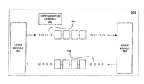
- FIG. 2 shows a diagram of the configurable signal path 110 in accordance with one embodiment of the present invention.
- the configurable signal path 110 includes a plurality of programmable latch/repeaters 201 - 204 .
- the configurable signal path of the present invention can optimize the number of programmable latch/repeaters included on the signal path 110 to most efficiently match a signal propagation delay related to an operating frequency of the digital integrated circuit.
- embodiments of the present invention are able to best optimize signal transmission paths between logic modules. For example, for given integrated circuit design, as transistor geometries decrease with successive process generations, and as transistors speed up by a substantial amount (e.g., in the order of 25-30% per generation), the wires that connect transistors can be configured for greater speed or lesser speed at the same rate.
- the wire cross-section decreases thereby increasing resistance, while the length decreases, decreasing resistance and capacitance.
- the wires speed up somewhat, but not as much as the transistors. This means that micro-architectures progressively have their timing dominated not by the logic depth of their combinational circuits, but rather by the transit time in the wires, especially those between functional blocks.
- Embodiments of the present invention accommodate both situations by implementing configurable signal paths, or “elastic pipelines,” that allow system designers to design a chip for very high frequency, while per-clock performance is not sacrificed when running at lower frequencies.
- FIG. 3 shows a diagram of a system 300 employing configurable signal paths (e.g., configurable signal paths 110 and 120 ) in accordance with one embodiment of the present invention.
- the configurable signal paths 110 and 120 effectively decouple the logic modules (e.g., logic blocks) 101 and 102 , and implement variable cycle transit signal paths between them.
- the logic modules 101 and 102 are decoupled, meaning that a set of defined protocols govern communication between blocks/units so that either side can take longer or shorter to accomplish its task, with the other side still operating properly.
- the protocol between the two modules 101 and 102 is such that the requesting module receives the reply/response/result an arbitrary number of cycles later and is told by the other module when the result is arriving.
- HyperTransport An example of such a protocol is the HyperTransport protocol. It is essentially a de-coupling protocol between two chips. The two chips use the protocol for inter-chip communication. HyperTransport happens to be external to a chip, but similar protocols can be used internally.
- each module when the modules 101 and 102 communicate over the configurable signal paths 110 and 120 in a decoupled protocol, each module has an internal register (or latch) to interface to the path.
- the originating module has a register within it from which the outgoing information starts its travel towards the other module.
- the receiving module has a register within it to receive the incoming information. This allows timing analysis to proceed locally within each of these modules, as the data is delivered locally (to the outgoing register or latch) and received locally (from the incoming register or latch).
- additional registers/latches e.g., programmable latch/repeaters
- programmable latch/repeaters are placed at periodic distances along the signal paths 110 and 120 . Since the protocol between the modules is decoupled, the system 300 will function properly whatever the number of intermediate programmable latch/repeaters ends up being linked into the path. Thus the placement and number of programmable latch/repeaters can conceptually wait until the last moment, when the timing of the slowest internal path is known. At that point the maximum distance between programmable latch/repeaters is known, and that determines how many are needed on a long path.
- the late choice allows a given design to not be penalized by over-pipelining of the protocol, at the expense of having to do placement of the programmable latch/repeaters at the last minute, which may be difficult.
- the configurable signal paths allow the distance to be decided a-priori, given the cycle time goal for the design, while ensuring the design is not inflexibly “stuck” with that number, even if timing within some module ended up forcing the design to run slower than the goal and higher per-clock performance could have been achieved by using fewer programmable latch/repeaters.
- a large number of programmable latch/repeaters are coupled along the path, wherein the number of programmable latch/repeaters is higher than the number required to meet the cycle time goals (e.g. every 1 ⁇ 3 cycle instead of every cycle).
- Each of the programmable latch/repeaters logically comprise a storage element and a buffer, where the storage element is used to optionally stage the signal by one cycle under external binary control.
- the programmable latch/repeater acts like a traditional buffer/repeater.
- the programmable latch/repeater acts like a latch or flip flop storage element followed by a buffer/repeater.
- the external binary control is provided by the configuration control module 310 .
- the chip is then designed according to this methodology. Then, depending on the target frequency as defined by either the achieved local timing of the communicating modules, or the system/platform constraints of operation, a sufficient set of programmable latch/repeaters are enabled to guarantee communication timing, but the rest are disabled and used as pass-through buffers.
- the external control provided by the control module 310 can be implemented using a number of different means.
- the control module 310 is software programmable to enable the variable number of programmable latch/repeaters.
- the chip resets with all the storage elements in the programmable latch/repeaters enabled, and then the control module 310 turns some of the programmable latch/repeaters off.
- Software control has the advantage that the chip can change its per-clock performance dynamically as operating conditions vary. For example, mobile chips often run at different frequencies in order to save power by using voltage/frequency scaling. This choice can be made by software as the chip operates.
- Dynamic control can also be used to accommodate performance differences due to temperature variations. Because lower temperatures mean lower resistance, wires speed up substantially at lower temperatures. Having dynamic control of the number of programmable latch/repeaters thus allows a software algorithm to increase per-clock performance at lower temperatures, but still meet frequency goals at higher temperatures. Thus a chip so designed that is placed in a very good thermal environment would perform better than if it was placed in a worse thermal environment but was still capable of running at the same frequency.
- software control is eliminated and the configuration control module 310 is omitted.
- late metal-level changes to the chip are built-in according to achieved frequency, thereby enabling or disabling the programmable latch/repeaters individually.
- on die fuses can be used to enable or disable the programmable latch/repeaters individually.
- external pins communicating which programmable latch/repeaters should be enabled or disabled can be used. In each case, at the higher frequencies, more programmable latch/repeaters would be required, but at the lower frequencies fewer would be required.
- FIG. 4 shows a diagram of an exemplary programmable latch/repeater 201 in accordance with one embodiment of the present invention.
- the programmable latch/repeater 201 comprises a storage element 401 (e.g., flop/register) and a multiplexer 402 controlled via a control input 405 .
- the multiplexer 402 selects the output of the storage element 401 and couples this output to an output buffer 403 .
- the multiplexer 402 selects the input and couples it directly to the output buffer 403 .
- the control input 405 determines whether the programmable latch/repeater 201 is on the signal path or off the signal path.
- FIG. 5 shows a diagram depicting a cache architecture 500 in accordance with one embodiment of the present invention.
- the architecture 500 comprises an L2 cache having a first block 501 having comparatively short propagation delay with respect to the access path 510 (e.g., to a CPU core), and a second block 502 having a comparatively long propagation delay with respect to the access path 510 .
- the cache 500 can be structured as a set of daisy-chained blocks where each block not only receives/sends data stored within it but also serves as a conduit for the data of subsequent blocks.
- FIG. 5 shows two such blocks 501 and 502 .
- the first block 501 would have to register/repeat the data from the second block 502 , as the wires between the blocks would take up a fair amount of time.
- the number of programmable latch/repeaters required would be lower and the cache would become faster in cycles.
- a large outer cache e.g., L2 cache
- Even larger cache architectures would realize a correspondingly larger benefit (e.g., L3 cache).
- FIG. 6 shows a diagram depicting logic execution architecture 600 in accordance with one embodiment of the present invention.
- the logic execution architecture 600 comprises a plurality of logic modules 601 - 603 coupled via a plurality of configurable signal paths 610 - 613 .
- the logic execution architecture 600 comprises a pipeline architecture of a processor (e.g., CPU).
- the processor becomes super-pipelined with long latencies between data-dependent operations of the logic modules 601 - 603 .
- the result of an ADD may not be available until two cycles later.
- the processor is pipelined in the ordinary fashion, with lower latencies between data-dependent operations.
- the result of an ADD would be available the following cycle.
- a buffer/repeater may not be needed in the middle of a data path.
- An optional latch/flip flop may be sufficient.
- a data path may be dominated by gate propagation delay and not have much wire component, so the buffer/repeater aspect is unnecessary.
- the concept is the same.
- a given design is over-pipelined, and some later time the number of programmable latch/repeaters, or latch/flip flops, required on the signal paths is chosen. For example, in a case where a given multiplier or adder can work in 2 cycles at low frequencies and 3 cycles at high frequencies, for the 2 cycle case, a latch/register would be coupled onto the signal path in the middle.
- latch/registers would be coupled every third.
- the elasticity attribute would be obtained by adding latch/registers every third, and in the middle (e.g., one extra latch/register over what the 3-cycle version would have).
- Late binding e.g., software, fuses, strapping pins, metal option, etc. selection would then be used to choose between 2 and 3 added latch/registers.
- these latches/registers would not a-priori need a repeater aspect.
- the logic execution architecture 600 comprises a special register protocol.
- Many CPUs have a special, slow, bus to read and write special (e.g., control) registers that are not accessed frequently.
- the configurable signal paths 610 - 613 would accommodate the larger number of needed cycles at high frequency and fewer number needed cycles at lower frequencies to access such special registers.
- the logic execution architecture 600 comprises a portion of a system-on-a-chip (SOC) design.
- SOC system-on-a-chip
- a “system-on a-chip” is a chip that includes a CPU and sufficient peripheral controller blocks to largely implement a full computer system by itself (with the possible and common exceptions of storage such as DRAM, FLASH/ROM for the initial program load, and disk).
- Typical systems on a chip are designed by taking a standard CPU core design as a “hard macro” which cannot be restructured and placing and connecting the peripheral controller blocks with it. This is problematic for high-performance CPUs due to the fact that their floorplan can severely constrain the ability of the SOC designer to place the peripheral controller blocks without making the chip overly wasteful (e.g., white space) and large.
- a CPU core designed using elastic pipelines in accordance with the present invention can be decomposed into a number of comparatively smaller hard macros that can be re-arranged as long as suitable additional programmable latch/repeaters are placed between the blocks. This is much different than being a single large monolithic hard macro. This allows the SOC designer to trade-off per-clock performance against the size and floor plan of the chip and time to market, without affecting the maximum frequency of the chip, or its correct operation.
Abstract
Description
Claims (22)
Priority Applications (3)
| Application Number | Priority Date | Filing Date | Title |
|---|---|---|---|
| US11/096,354 US7724027B2 (en) | 2005-03-31 | 2005-03-31 | Method and system for elastic signal pipelining |
| PCT/US2006/011661 WO2006105303A1 (en) | 2005-03-31 | 2006-03-29 | A method and system for elastic signal pipelining |
| TW095111222A TWI386849B (en) | 2005-03-31 | 2006-03-30 | A method and system for elastic signal pipelining |
Applications Claiming Priority (1)
| Application Number | Priority Date | Filing Date | Title |
|---|---|---|---|
| US11/096,354 US7724027B2 (en) | 2005-03-31 | 2005-03-31 | Method and system for elastic signal pipelining |
Publications (2)
| Publication Number | Publication Date |
|---|---|
| US20060220678A1 US20060220678A1 (en) | 2006-10-05 |
| US7724027B2 true US7724027B2 (en) | 2010-05-25 |
Family
ID=37053716
Family Applications (1)
| Application Number | Title | Priority Date | Filing Date |
|---|---|---|---|
| US11/096,354 Active 2025-05-21 US7724027B2 (en) | 2005-03-31 | 2005-03-31 | Method and system for elastic signal pipelining |
Country Status (3)
| Country | Link |
|---|---|
| US (1) | US7724027B2 (en) |
| TW (1) | TWI386849B (en) |
| WO (1) | WO2006105303A1 (en) |
Cited By (1)
| Publication number | Priority date | Publication date | Assignee | Title |
|---|---|---|---|---|
| US20120099622A1 (en) * | 2010-10-20 | 2012-04-26 | Masleid Robert P | Repeater circuit with multiplexer and state element functionality |
Families Citing this family (17)
| Publication number | Priority date | Publication date | Assignee | Title |
|---|---|---|---|---|
| US7236009B1 (en) | 2004-12-01 | 2007-06-26 | Andre Rohe | Operational time extension |
| US7428721B2 (en) * | 2004-12-01 | 2008-09-23 | Tabula, Inc. | Operational cycle assignment in a configurable IC |
| US7724027B2 (en) | 2005-03-31 | 2010-05-25 | Rozas Guillermo J | Method and system for elastic signal pipelining |
| US20070013425A1 (en) * | 2005-06-30 | 2007-01-18 | Burr James B | Lower minimum retention voltage storage elements |
| US7663408B2 (en) * | 2005-06-30 | 2010-02-16 | Robert Paul Masleid | Scannable dynamic circuit latch |
| US7256634B2 (en) * | 2005-07-06 | 2007-08-14 | Transmeta Corporation | Elastic pipeline latch with a safe mode |
| US7372297B1 (en) | 2005-11-07 | 2008-05-13 | Tabula Inc. | Hybrid interconnect/logic circuits enabling efficient replication of a function in several sub-cycles to save logic and routing resources |
| US7679401B1 (en) | 2005-12-01 | 2010-03-16 | Tabula, Inc. | User registers implemented with routing circuits in a configurable IC |
| US7495466B1 (en) * | 2006-06-30 | 2009-02-24 | Transmeta Corporation | Triple latch flip flop system and method |
| US7525344B2 (en) | 2007-03-20 | 2009-04-28 | Tabula, Inc. | Configurable IC having a routing fabric with storage elements |
| US8863067B1 (en) | 2008-02-06 | 2014-10-14 | Tabula, Inc. | Sequential delay analysis by placement engines |
| US8166435B2 (en) * | 2008-06-26 | 2012-04-24 | Tabula, Inc. | Timing operations in an IC with configurable circuits |
| US8674721B2 (en) * | 2008-09-17 | 2014-03-18 | Tabula, Inc. | Controllable storage elements for an IC |
| US8760193B2 (en) | 2011-07-01 | 2014-06-24 | Tabula, Inc. | Configurable storage elements |
| US9148151B2 (en) | 2011-07-13 | 2015-09-29 | Altera Corporation | Configurable storage elements |
| US8984464B1 (en) | 2011-11-21 | 2015-03-17 | Tabula, Inc. | Detailed placement with search and repair |
| CN111316234B (en) * | 2017-09-12 | 2024-03-12 | 恩倍科微公司 | Very low power microcontroller system |
Citations (26)
| Publication number | Priority date | Publication date | Assignee | Title |
|---|---|---|---|---|
| US5453708A (en) | 1995-01-04 | 1995-09-26 | Intel Corporation | Clocking scheme for latching of a domino output |
| US5610548A (en) | 1995-09-08 | 1997-03-11 | International Business Machines Corporation | Split drive clock buffer |
| US5721886A (en) * | 1995-11-30 | 1998-02-24 | Ncr Corporation | Synchronizer circuit which controls switching of clocks based upon synchronicity, asynchronicity, or change in frequency |
| US5880612A (en) | 1996-10-17 | 1999-03-09 | Samsung Electronics Co., Ltd. | Signal de-skewing using programmable dual delay-locked loop |
| US6025738A (en) | 1997-08-22 | 2000-02-15 | International Business Machines Corporation | Gain enhanced split drive buffer |
| US6081462A (en) * | 1997-08-22 | 2000-06-27 | Micron Technology, Inc. | Adjustable delay circuit for setting the speed grade of a semiconductor device |
| US6133759A (en) | 1998-06-16 | 2000-10-17 | International Business Machines Corp. | Decoupled reset dynamic logic circuit |
| US6154045A (en) | 1998-12-22 | 2000-11-28 | Intel Corporation | Method and apparatus for reducing signal transmission delay using skewed gates |
| US6188259B1 (en) | 1999-11-03 | 2001-02-13 | Sun Microsystems, Inc. | Self-reset flip-flop with self shut-off mechanism |
| JP2001188638A (en) | 2000-01-05 | 2001-07-10 | Mitsubishi Electric Corp | Bi-directional bus circuit |
| WO2002015195A2 (en) | 2000-08-14 | 2002-02-21 | Rambus, Inc. | Method and apparatus for controlling a read valid window of a synchronous memory device |
| US20020039347A1 (en) | 2000-06-30 | 2002-04-04 | Kazuoki Matsugatani | Communication device having delay information calculating function |
| US20020087930A1 (en) | 2000-12-28 | 2002-07-04 | Nec Corporation | Scan flip-flop circuit capable of guaranteeing normal operation |
| US6466063B2 (en) | 2001-03-20 | 2002-10-15 | Taiwan Semiconductor Manufacturing Co., Ltd. | Push-pull output buffer with gate voltage feedback loop |
| US6577176B1 (en) | 2002-06-12 | 2003-06-10 | Fujitsu Limited | Complement reset latch |
| US6630851B2 (en) | 2001-06-29 | 2003-10-07 | Fujitsu Limited | Low latency clock distribution |
| US6664807B1 (en) | 2002-01-22 | 2003-12-16 | Xilinx, Inc. | Repeater for buffering a signal on a long data line of a programmable logic device |
| US20040032290A1 (en) | 2002-07-09 | 2004-02-19 | Ip-First Llc | Teacher-pupil flip-flop |
| US6799280B1 (en) * | 2000-01-04 | 2004-09-28 | Advanced Micro Devices, Inc. | System and method for synchronizing data transfer from one domain to another by selecting output data from either a first or second storage device |
| US20050195642A1 (en) | 2004-03-04 | 2005-09-08 | Schmitt Peer G. | Ternary bit line signaling |
| US20050206432A1 (en) | 2004-03-22 | 2005-09-22 | Mitsubishi Denki Kabushiki Kaisha | Level conversion circuit and serial/parallel conversion circuit with level conversion function |
| US6988215B2 (en) * | 2001-09-14 | 2006-01-17 | Medtronic, Inc. | Method and apparatus for synchronization of clock domains |
| US7076682B2 (en) | 2004-05-04 | 2006-07-11 | International Business Machines Corp. | Synchronous pipeline with normally transparent pipeline stages |
| US20060220678A1 (en) | 2005-03-31 | 2006-10-05 | Transmeta Corporation | Method and system for elastic signal pipelining |
| US7119580B2 (en) | 2004-06-08 | 2006-10-10 | Transmeta Corporation | Repeater circuit with high performance repeater mode and normal repeater mode |
| US7256634B2 (en) | 2005-07-06 | 2007-08-14 | Transmeta Corporation | Elastic pipeline latch with a safe mode |
Family Cites Families (5)
| Publication number | Priority date | Publication date | Assignee | Title |
|---|---|---|---|---|
| US6604807B1 (en) * | 1999-02-18 | 2003-08-12 | Hewlett-Packard Company | Method and apparatus for detecting anomalous nozzles in an ink jet printer device |
| JP2002014914A (en) * | 2000-06-29 | 2002-01-18 | Toshiba Corp | Function block |
| US6848060B2 (en) * | 2001-02-27 | 2005-01-25 | International Business Machines Corporation | Synchronous to asynchronous to synchronous interface |
| JP2003316566A (en) * | 2002-04-24 | 2003-11-07 | Matsushita Electric Ind Co Ltd | Pipeline processor |
| JP2004062281A (en) * | 2002-07-25 | 2004-02-26 | Nec Micro Systems Ltd | Pipeline processor and pipeline operation control method |
-
2005
- 2005-03-31 US US11/096,354 patent/US7724027B2/en active Active
-
2006
- 2006-03-29 WO PCT/US2006/011661 patent/WO2006105303A1/en active Application Filing
- 2006-03-30 TW TW095111222A patent/TWI386849B/en active
Patent Citations (28)
| Publication number | Priority date | Publication date | Assignee | Title |
|---|---|---|---|---|
| US5453708A (en) | 1995-01-04 | 1995-09-26 | Intel Corporation | Clocking scheme for latching of a domino output |
| US5610548A (en) | 1995-09-08 | 1997-03-11 | International Business Machines Corporation | Split drive clock buffer |
| US5721886A (en) * | 1995-11-30 | 1998-02-24 | Ncr Corporation | Synchronizer circuit which controls switching of clocks based upon synchronicity, asynchronicity, or change in frequency |
| US5880612A (en) | 1996-10-17 | 1999-03-09 | Samsung Electronics Co., Ltd. | Signal de-skewing using programmable dual delay-locked loop |
| US6025738A (en) | 1997-08-22 | 2000-02-15 | International Business Machines Corporation | Gain enhanced split drive buffer |
| US6081462A (en) * | 1997-08-22 | 2000-06-27 | Micron Technology, Inc. | Adjustable delay circuit for setting the speed grade of a semiconductor device |
| US6133759A (en) | 1998-06-16 | 2000-10-17 | International Business Machines Corp. | Decoupled reset dynamic logic circuit |
| US6154045A (en) | 1998-12-22 | 2000-11-28 | Intel Corporation | Method and apparatus for reducing signal transmission delay using skewed gates |
| US6188259B1 (en) | 1999-11-03 | 2001-02-13 | Sun Microsystems, Inc. | Self-reset flip-flop with self shut-off mechanism |
| US6799280B1 (en) * | 2000-01-04 | 2004-09-28 | Advanced Micro Devices, Inc. | System and method for synchronizing data transfer from one domain to another by selecting output data from either a first or second storage device |
| JP2001188638A (en) | 2000-01-05 | 2001-07-10 | Mitsubishi Electric Corp | Bi-directional bus circuit |
| US20020039347A1 (en) | 2000-06-30 | 2002-04-04 | Kazuoki Matsugatani | Communication device having delay information calculating function |
| WO2002015195A2 (en) | 2000-08-14 | 2002-02-21 | Rambus, Inc. | Method and apparatus for controlling a read valid window of a synchronous memory device |
| US20020087930A1 (en) | 2000-12-28 | 2002-07-04 | Nec Corporation | Scan flip-flop circuit capable of guaranteeing normal operation |
| US6466063B2 (en) | 2001-03-20 | 2002-10-15 | Taiwan Semiconductor Manufacturing Co., Ltd. | Push-pull output buffer with gate voltage feedback loop |
| US6630851B2 (en) | 2001-06-29 | 2003-10-07 | Fujitsu Limited | Low latency clock distribution |
| US6988215B2 (en) * | 2001-09-14 | 2006-01-17 | Medtronic, Inc. | Method and apparatus for synchronization of clock domains |
| US6664807B1 (en) | 2002-01-22 | 2003-12-16 | Xilinx, Inc. | Repeater for buffering a signal on a long data line of a programmable logic device |
| US6577176B1 (en) | 2002-06-12 | 2003-06-10 | Fujitsu Limited | Complement reset latch |
| US6731140B2 (en) | 2002-06-12 | 2004-05-04 | Fujitsu Limited | Complement reset multiplexer latch |
| US6956405B2 (en) | 2002-07-09 | 2005-10-18 | Ip-First, Llc | Teacher-pupil flip-flop |
| US20040032290A1 (en) | 2002-07-09 | 2004-02-19 | Ip-First Llc | Teacher-pupil flip-flop |
| US20050195642A1 (en) | 2004-03-04 | 2005-09-08 | Schmitt Peer G. | Ternary bit line signaling |
| US20050206432A1 (en) | 2004-03-22 | 2005-09-22 | Mitsubishi Denki Kabushiki Kaisha | Level conversion circuit and serial/parallel conversion circuit with level conversion function |
| US7076682B2 (en) | 2004-05-04 | 2006-07-11 | International Business Machines Corp. | Synchronous pipeline with normally transparent pipeline stages |
| US7119580B2 (en) | 2004-06-08 | 2006-10-10 | Transmeta Corporation | Repeater circuit with high performance repeater mode and normal repeater mode |
| US20060220678A1 (en) | 2005-03-31 | 2006-10-05 | Transmeta Corporation | Method and system for elastic signal pipelining |
| US7256634B2 (en) | 2005-07-06 | 2007-08-14 | Transmeta Corporation | Elastic pipeline latch with a safe mode |
Non-Patent Citations (8)
| Title |
|---|
| Advisory Action Mailed Feb. 26, 2009; 11893221; TRAN-P443C1. |
| Final Office Action Mailed Dec. 4, 2008; 11893221; TRAN-P443C1. |
| Final Office Action Mailed May 8, 2009; Serial No. 11893221; TRAN-P443C1. |
| Non-Final Office Action Mailed Feb. 1, 2008; 11893221; TRAN-P443C1. |
| Non-Final Office Action Mailed Jun. 27, 2008; 11893221; TRAN-P443C1. |
| Notice of Allowance Mailed Dec. 15, 2006; 11176918; TRAN-P443. |
| Notice of Allowance Mailed Mar. 30, 2007; 11176918; TRAN-P443. |
| Webster's II Riverside University Dictionary; p. 406, 407; 1984. |
Cited By (2)
| Publication number | Priority date | Publication date | Assignee | Title |
|---|---|---|---|---|
| US20120099622A1 (en) * | 2010-10-20 | 2012-04-26 | Masleid Robert P | Repeater circuit with multiplexer and state element functionality |
| US8525550B2 (en) * | 2010-10-20 | 2013-09-03 | Robert P. Masleid | Repeater circuit with multiplexer and state element functionality |
Also Published As
| Publication number | Publication date |
|---|---|
| TW200705265A (en) | 2007-02-01 |
| WO2006105303A1 (en) | 2006-10-05 |
| US20060220678A1 (en) | 2006-10-05 |
| TWI386849B (en) | 2013-02-21 |
Similar Documents
| Publication | Publication Date | Title |
|---|---|---|
| US7724027B2 (en) | Method and system for elastic signal pipelining | |
| US7737749B1 (en) | Elastic pipeline latch with a safe mode | |
| US7266632B2 (en) | Programmable logic device including programmable interface core and central processing unit | |
| US6810460B1 (en) | AMBA bus off-chip bridge | |
| US8484523B2 (en) | Sequential digital circuitry with test scan | |
| US20060044925A1 (en) | Limited output address register technique providing selectively variable write latency in DDR2 (double data rate two) integrated circuit memory devices | |
| US7461187B2 (en) | Bus system and data transfer method | |
| US20070198758A1 (en) | Bus apparatus, bus system and information transferring method | |
| US7296175B2 (en) | System on a chip bus with automatic pipeline stage insertion for timing closure | |
| US8418092B2 (en) | Source-synchronous data link for system-on-chip design | |
| US7054971B2 (en) | Interface between a host and a slave device having a latency greater than the latency of the host | |
| US20040248353A1 (en) | Processor and semiconductor integrated circuit | |
| US10922129B2 (en) | Operation processing device and control method of operation processing device | |
| US20210124709A1 (en) | Communication system and operation method | |
| Nawrath et al. | FPGA-based implementation of APB/SPI bridge | |
| JP4799137B2 (en) | Bus system | |
| US20050013356A1 (en) | Methods and apparatus for providing test access to asynchronous circuits and systems | |
| KR101621760B1 (en) | A pipeline circuit apparatus having asynchronous clock | |
| US6202113B1 (en) | Bank register circuit for a multiply accumulate circuit | |
| CN113515910B (en) | AXI bus-based data preprocessing method | |
| JP2007219962A (en) | Semiconductor integrated circuit device | |
| US10270433B1 (en) | Master-slave clock generation circuit | |
| US20120229181A1 (en) | Asynchronous circuit | |
| JP2006209162A (en) | Logic verification device | |
| JP2576262B2 (en) | Information processing device |
Legal Events
| Date | Code | Title | Description |
|---|---|---|---|
| AS | Assignment |
Owner name: TRANSMETA CORPORATION, CALIFORNIA Free format text: ASSIGNMENT OF ASSIGNORS INTEREST;ASSIGNORS:ROZAS, GUILLERMO J.;MASLEID, ROBERT;REEL/FRAME:016452/0273 Effective date: 20050331 Owner name: TRANSMETA CORPORATION,CALIFORNIA Free format text: ASSIGNMENT OF ASSIGNORS INTEREST;ASSIGNORS:ROZAS, GUILLERMO J.;MASLEID, ROBERT;REEL/FRAME:016452/0273 Effective date: 20050331 |
|
| AS | Assignment |
Owner name: TRANSMETA LLC, CALIFORNIA Free format text: MERGER;ASSIGNOR:TRANSMETA CORPORATION;REEL/FRAME:022454/0522 Effective date: 20090127 Owner name: TRANSMETA LLC,CALIFORNIA Free format text: MERGER;ASSIGNOR:TRANSMETA CORPORATION;REEL/FRAME:022454/0522 Effective date: 20090127 |
|
| AS | Assignment |
Owner name: INTELLECTUAL VENTURE FUNDING LLC, NEVADA Free format text: ASSIGNMENT OF ASSIGNORS INTEREST;ASSIGNOR:TRANSMETA LLC;REEL/FRAME:023268/0771 Effective date: 20090128 Owner name: INTELLECTUAL VENTURE FUNDING LLC,NEVADA Free format text: ASSIGNMENT OF ASSIGNORS INTEREST;ASSIGNOR:TRANSMETA LLC;REEL/FRAME:023268/0771 Effective date: 20090128 |
|
| STCF | Information on status: patent grant |
Free format text: PATENTED CASE |
|
| FPAY | Fee payment |
Year of fee payment: 4 |
|
| AS | Assignment |
Owner name: INTELLECTUAL VENTURES HOLDING 81 LLC, NEVADA Free format text: MERGER;ASSIGNOR:INTELLECTUAL VENTURE FUNDING LLC;REEL/FRAME:036711/0160 Effective date: 20150827 |
|
| AS | Assignment |
Owner name: INTELLECTUAL VENTURES HOLDING 81 LLC, NEVADA Free format text: CORRECTIVE ASSIGNMENT TO CORRECT THE ASSIGNOR'S NAME PREVIOUSLY RECORDED AT REEL: 036711 FRAME: 0160. ASSIGNOR(S) HEREBY CONFIRMS THE MERGER;ASSIGNOR:INTELLECTUAL VENTURES FUNDING LLC;REEL/FRAME:036797/0356 Effective date: 20150827 |
|
| MAFP | Maintenance fee payment |
Free format text: PAYMENT OF MAINTENANCE FEE, 8TH YEAR, LARGE ENTITY (ORIGINAL EVENT CODE: M1552) Year of fee payment: 8 |
|
| MAFP | Maintenance fee payment |
Free format text: PAYMENT OF MAINTENANCE FEE, 12TH YEAR, LARGE ENTITY (ORIGINAL EVENT CODE: M1553); ENTITY STATUS OF PATENT OWNER: LARGE ENTITY Year of fee payment: 12 |