US7474106B2 - Semiconductor device including fuse and method for testing the same capable of suppressing erroneous determination - Google Patents
Semiconductor device including fuse and method for testing the same capable of suppressing erroneous determination Download PDFInfo
- Publication number
- US7474106B2 US7474106B2 US11/514,235 US51423506A US7474106B2 US 7474106 B2 US7474106 B2 US 7474106B2 US 51423506 A US51423506 A US 51423506A US 7474106 B2 US7474106 B2 US 7474106B2
- Authority
- US
- United States
- Prior art keywords
- fuse
- resistance value
- voltage
- power supply
- measuring terminal
- Prior art date
- Legal status (The legal status is an assumption and is not a legal conclusion. Google has not performed a legal analysis and makes no representation as to the accuracy of the status listed.)
- Expired - Fee Related, expires
Links
Images


Classifications
-
- G—PHYSICS
- G11—INFORMATION STORAGE
- G11C—STATIC STORES
- G11C29/00—Checking stores for correct operation ; Subsequent repair; Testing stores during standby or offline operation
- G11C29/02—Detection or location of defective auxiliary circuits, e.g. defective refresh counters
-
- G—PHYSICS
- G11—INFORMATION STORAGE
- G11C—STATIC STORES
- G11C17/00—Read-only memories programmable only once; Semi-permanent stores, e.g. manually-replaceable information cards
- G11C17/14—Read-only memories programmable only once; Semi-permanent stores, e.g. manually-replaceable information cards in which contents are determined by selectively establishing, breaking or modifying connecting links by permanently altering the state of coupling elements, e.g. PROM
- G11C17/143—Read-only memories programmable only once; Semi-permanent stores, e.g. manually-replaceable information cards in which contents are determined by selectively establishing, breaking or modifying connecting links by permanently altering the state of coupling elements, e.g. PROM using laser-fusible links
-
- G—PHYSICS
- G11—INFORMATION STORAGE
- G11C—STATIC STORES
- G11C29/00—Checking stores for correct operation ; Subsequent repair; Testing stores during standby or offline operation
- G11C29/02—Detection or location of defective auxiliary circuits, e.g. defective refresh counters
- G11C29/027—Detection or location of defective auxiliary circuits, e.g. defective refresh counters in fuses
-
- G—PHYSICS
- G11—INFORMATION STORAGE
- G11C—STATIC STORES
- G11C29/00—Checking stores for correct operation ; Subsequent repair; Testing stores during standby or offline operation
- G11C29/02—Detection or location of defective auxiliary circuits, e.g. defective refresh counters
- G11C29/028—Detection or location of defective auxiliary circuits, e.g. defective refresh counters with adaption or trimming of parameters
Definitions
- the present invention relates to a semiconductor device including at least one trimming detection circuit formed by a fuse as a trimming element and a method for testing the trimming detection circuit.
- a trimming detection circuit formed by an electrically-trimmed trimming element showing logic “1” or “0” may be incorporated into a semiconductor device.
- a trimming element is a laser fuse trimmed by laser, a Zener diode trimmed by Zener zap or a so-called electric (E)-fuse trimmed by supplying a blowing current thereto.
- an incomplete disconnection state may occur. For example, after a fuse is trimmed by laser, a melted remainder of the fuse may be present in the proximity of the trimmed fuse, so that the trimmed fuse would be in an incomplete disconnection state.
- a semiconductor device including such an incomplete trimming detection circuit should be scrapped before the shipping.
- a prior art semiconductor device includes a trimming detection circuit which is constructed by a series arrangement of a resistor and a fuse connected between a power supply terminal and a ground terminal, a series arrangement of a testing resistor and an n-channel MOS transistor connected in parallel with the fuse, and a determination circuit formed by an inverter connected to a node between the resistor and the fuse to determine whether the fuse is connected or disconnected (see: JP-10-62477 A).
- the testing resistor In a normal mode where a control signal applied to the gate of the MOS transistor is low, the testing resistor is disconnected from the node. On the other hand, in a test mode where the control signal applied to the gate of the MOS transistor is high, the testing resistor is connected to the node. As a result, the determination circuit can determine the incomplete disconnection state fuse as a disconnection state fuse. This will be explained later in detail.
- the resistance value of the incomplete disconnection state fuse actually depends upon the environmental factors such as the voltage at the power supply terminal, the temperature and so on and the time aging deviation thereof, the resistance value of the incomplete disconnection state fuse varies greatly, so that the determination circuit cannot always determine the incomplete disconnection state fuse as a disconnection state.
- the trimming detection circuit is constructed by a current supplying element, a series arrangement of a fuse and a switch element, and a determination circuit.
- the current supplying element and the series arrangement are connected in series between the measuring terminal and the one of the first and second power supply terminals.
- the determination circuit has an input connected to a node between the current supplying element and the series arrangement and is adapted to determine whether the fuse is in a connection state or in a disconnection state. A voltage at the other of the first and second power supply terminals is applied to the measuring terminal in a normal mode.
- FIG. 1 is a circuit diagram illustrating a prior art semiconductor device including a trimming detection circuit
- FIG. 2 is a circuit diagram illustrating a first embodiment of the semiconductor device according to the present invention.
- FIGS. 3A and 3B are circuit diagrams for explaining the manufacturing steps of the semiconductor device of FIG. 2 ;
- FIG. 4 is a flowchart for testing the semiconductor device of FIG. 3B ;
- FIG. 5 and FIGS. 6A and 6B are modifications of the flowchart of FIG. 4 ;
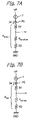
- FIGS. 7A and 7B are circuit diagrams for explaining the flowchart of FIGS. 6A and 6B ;
- FIG. 8 is a circuit diagram illustrating a second embodiment of the semiconductor device according to the present invention.
- FIGS. 9 and 10 are flowcharts for testing the semiconductor device of FIG. 8 ;
- FIG. 11 is a circuit diagram illustrating a third embodiment of the semiconductor device according to the present invention.
- FIGS. 12A , 12 B and 12 C are circuit diagrams of modifications of the semiconductor device of FIG. 2 .
- a trimming detection circuit is constructed by a series arrangement of a resistor 101 and a fuse 102 connected between a power supply terminal V DD and a ground terminal GND. Also, the trimming detection circuit is constructed by a series arrangement of a testing resistor 103 and an n-channel MOS transistor 104 connected in parallel with the fuse 102 . Further, the trimming detection circuit is constructed by a determination circuit 105 formed by an inverter connected to a node N 101 between the resistor 101 and the fuse 102 , to thereby determine whether the fuse 102 is connected or disconnected.
- V DD and GND also designate voltages applied to the terminals V DD and GND, respectively.
- the resistance values of the resistor 101 and the testing resistor 103 are 2R and 4R, respectively, and the threshold voltage of the determination circuit 105 is V DD /2.
- the resistance value of the fuse 102 is R in a connection state, HZ (high impedance) in a complete disconnection state and about 2R in an incomplete disconnection state.
- the testing resistor 103 is disconnected from the node N 101 . Therefore, if the fuse 102 is in a connection state, the voltage at the node N 101 is (1 ⁇ 3) ⁇ V DD , so that the output V out of the determination circuit 103 is “1” (high level). Also, if the fuse 102 is in a complete disconnection state, the voltage at the node N 101 is V DD , so that the output V out of the determination circuit 105 is “0” (low level). Further, if the fuse 102 is in an incomplete disconnection state, the voltage at the node N 101 is about (1 ⁇ 2) ⁇ V DD , so that the output V out of the determination circuit 105 is unstable.
- the testing resistor 103 is connected to the node N 101 . Therefore, if the fuse 102 is in a connection state, the voltage at the node N 101 is ( 1/7) ⁇ V DD , so that the output V out of the determination circuit 103 is “1” (high level). Also, if the fuse 102 is in a complete disconnection state, the voltage at the node N 101 is (2 ⁇ 3) ⁇ V DD , so that the output V out of the determination circuit 105 is “0” (low level).
- the determination circuit 105 can determine the incomplete disconnection state fuse 102 as a disconnection state fuse.
- the resistance value of the incomplete disconnection state fuse 102 actually depends upon the environmental factors such as the voltage at the power supply terminal V DD , the temperature and so on and the time aging deviation thereof, the resistance value of the incomplete disconnection state fuse 102 greatly varies, so that the determination circuit 105 cannot always determine the incomplete disconnection state fuse 102 as a disconnection state.
- this semiconductor device includes one trimming detection circuit which is constructed by a resistor 1 and a series arrangement of a fuse 2 and an n-channel MOS transistor 3 connected in series between a measuring terminal (pad) PO and a ground terminal (pad) GND.
- the trimming detection circuit is constructed by a determination circuit 4 formed by an inverter connected to a node NO between the resistor 1 and the series arrangement of the fuse 3 and the n-channel MOS transistor 3 , to thereby determine whether the fuse 2 is connected or disconnected.
- the inverter of the determination circuit 4 has a threshold voltage of V DD /2, for example.
- a power supply voltage V DD is applied to the measuring terminal (pad) PO and a control signal CNT applied to the gate of the MOS transistor 3 is high, the fuse 2 is connected to the ground terminal GND. Therefore, if the fuse 2 is in a connection state, the voltage at the node NO is GND, so that the output V out of the determination circuit 4 is “1” (high level). Also, if the fuse 2 is in a complete disconnection state, the voltage at the node NO is V DD , so that the output V out of the determination circuit 4 is “0” (low level).
- control signal CNT applied to the gate of the MOS transistor 1 is also high; however, in this case, a current detector of a tester along with a test voltage VF is connected to the measuring terminal PO.
- FIGS. 3A and 3B A method for manufacturing the semiconductor device of FIG. 2 is explained next with reference to FIGS. 3A and 3B .
- the resistor 1 , the series arrangement of the fuse 2 and the n-channel MOS transistor 3 , and the determination circuit 4 are formed in a semiconductor substrate (not shown). Also, the gate of the MOS transistor 3 is connected via another fuse 5 to a terminal (pad) AO which is not used for testing the trimming detection circuit. Further, the gate of the NOS transistor 3 is connected via a pull-up resistor 6 to the power supply terminal (pad) V DD . Therefore, after the fuse 5 is disconnected by a trimming process, the control signal CNT is always high-to turn ON the MOS transistor 3 .
- a current detector 7 of a tester to which a test voltage VF is applied is connected to the measuring terminal (pad) PO using a probe (not shown), and the tester is also connected to other pads including the power supply terminal (pad) V DD , the ground terminal (pad) GND, the address signal terminal (pad) AO and so on.
- the tester also can supply a blowing current via a fuse blowing circuit (not shown) to the fuse 2 , so that the fuse 2 can be melted by the electromigration phenomenon.
- Whether the fuse 2 is in a connection state, in a complete disconnection state or in an incomplete disconnection state and whether the determination circuit (inverter) 4 is normal or abnormal are determined by a test routine as shown in FIG. 4 .
- the test routine of FIG. 4 is stored in the memory of the tester.
- steps 401 to 403 perform an inverter test upon the determination circuit (inverter) 4
- steps 404 to 411 perform a fuse test upon the fuse 2 .
- the control signal CNT is made “0” (low) by causing the voltage at the terminal (pad) AO to be “0” (low).
- the voltage at the node NO is VF.
- the threshold voltage V th of the determination circuit 4 is detected by changing the voltage VF.
- V th is detected when the output V out is switched from high to low or vice versa.
- step 403 it is determined whether or not the detected threshold voltage V th is within a normal range such as from V DD /2 ⁇ to V DD /2+ ⁇ where ⁇ is a definite value. As a result, only when the detected threshold voltage V th is within the normal range, does the control proceed to step 404 . Otherwise, the control proceeds to a failure mode which would scrap the device.
- the testing operation of the determination circuit (inverter) 4 can be carried out regardless of whether the fuse 2 is connected or disconnected. Therefore, test debug can be effectively carried out before the fuse 2 is disconnected.
- V DD ⁇ or V DD + ⁇ can be applied to the node N 0 , so that the inverter test operation can be carried out by determining whether V out is “1” (high level) or “0” (low level).
- a fuse blowing process is performed upon the fuse 2 by supplying a fuse blowing current to the fuse 2 via a fuse blowing circuit (not shown).
- control signal CNT is made “1” (high level) by causing the voltage at the terminal (pad) AO to be high.
- a definite voltage is applied as the test voltage VF to the measuring terminal (pad) PO.
- a current IM is fetched from the current detector 7 flowing through a circuit formed by the resistor 1 , the fuse 2 and the MOS transistor 3 .
- a resistance value R fuse of the fuse 2 is calculated by R fuse ⁇ VF/IM ⁇ R1 ⁇ R3
- R 1 is a resistance value of the resistor 1 ;
- R 3 is an ON-resistance value of the MOS transistor 3 . Note that, generally, since R 3 ⁇ R 1 , the ON-resistance value R 3 can be omitted. In this case, since the resistance value R 1 of the resistor 1 is determined in advance, the resistance value R fuse can be determined.
- step 409 it is determined whether or not the resistance value R fuse of the fuse 2 is within a normal range defined by values r 1 and r 2 (r 1 ⁇ r 2 ). That is, if R fuse ⁇ r 1 , the fuse 2 is deemed to be in a connection state, and if R fuse ⁇ r 2 , the fuse 2 is deemed to be in a complete disconnection state. Therefore, the control proceeds to a pass mode. On the other hand, if r 1 ⁇ R fuse ⁇ r 2 , the fuse 2 is deemed to be in an incomplete disconnection state, so that the control returns via steps 410 and 411 to step 404 which carries out another fuse blowing process.
- steps 410 and 411 can be omitted; in this case, if the determination at step 409 is affirmative (r 1 ⁇ R fuse ⁇ r 2 ), the control always proceeds to the failure mode.
- a fuse blowing process is performed upon the fuse 5 using a fuse blowing circuit (not shown), so that the control signal CNT can always be made high by the pull-up resistor 6 .
- the MOS transistor 3 can always be turned ON. Also, the tester along with the probes is removed from the device, thus obtaining the semiconductor device of FIG. 2 .
- steps 401 to 403 can be carried out after steps 404 to 411 are carried out.
- steps 501 and 502 are provided instead of steps 401 , 402 and 403 of FIG. 4 .
- FIG. 6 which is another modification of the flowchart of FIG. 4 , steps 601 to 604 are added to the steps of FIG. 4 , and steps 408 A and 408 B are provided instead of step 408 of FIG. 4 .
- a resistance value R uncut of a circuit formed by the resistor 1 , the fuse 2 and the MOS transistor 3 before the fuse 2 is disconnected. That is, at step 601 , the control signal CNT is made “1” (high level) by causing the voltage at the terminal (pad) AO to be high. Next, at step 602 , a definite voltage is applied as the voltage VF to the measuring terminal (pad) PO. Next, at step 603 , a current IM is fetched from the current detector 7 flowing through the circuit formed by the resistor 1 , the fuse 2 and the MOS transistor 3 . Next, at step 604 , the resistance value R uncut of this circuit is calculated by R uncut ⁇ VF/IM
- a resistance value R cut of the circuit formed by the resistor 1 , the fuse 2 and the MOS transistor 3 after the fuse 2 is disconnected. That is, at step 404 , as occasion demands, a fuse blowing process is performed upon the fuse 2 by supplying a fuse blowing current to the fuse 2 via a fuse blowing circuit (not shown).
- the control signal CNT is made “1” (high) by causing the voltage at the terminal (pad) AO to be high.
- a definite voltage is applied as the test voltage VF to the measuring terminal (pad) PO.
- a current IM is fetched from the current detector 7 flowing through the circuit formed by the resistor 1 , the fuse 2 and the MOS transistor 3 .
- the resistance value R cut of this circuit is calculated by R cut ⁇ VF/IM
- the resistance value R fuse of the fuse 2 is calculated by R fuse ⁇ R cut ⁇ R uncut
- the resistance value R cutfuse or R fuse can be calculated by the above-mentioned formula.
- step 409 it can be determined whether or not the fuse 2 is in an incomplete disconnection state.
- steps 501 and 502 of FIG. 5 can be provided instead of steps 401 , 402 and 403 .
- this semiconductor device includes a plurality of trimming detection circuits each of which is constructed by a resistor 1 -i and a series arrangement of a fuse 2 -i and an n-channel MOS transistor 3 -i connected in series between a measuring terminal (pad) PO and a ground terminal (pad) GND, and a determination circuit 4 -i formed by an inverter connected to a node Ni between the resistor 1 -i and the series arrangement of the fuse 3 -i and the n-channel MOS transistor 3 -i , to thereby determine whether the fuse 2 -i is connected or disconnected, where i is 1, 2, . . . , n.
- the inverter of the determination circuit 4 -i has a threshold voltage of V DD /2.
- a terminal (pad), a fuse and a pull-up resistor (not shown) the same as the address-terminal AO, the fuse 5 and the pull-up resistor 6 of FIGS. 3A and 3B are connected to each gate of the MOS transistors 3 - 1 , 3 - 2 , . . . , 3 -n.
- the power supply voltage V DD is applied to the measuring terminal (pad) PO, and control signals CNT 1 , CNT 2 , . . . , CNTn applied to the gates of the MOS transistor 3 - 1 , 3 - 2 , . . . , 3 -n are high, so that the fuses 2 - 1 , 2 - 2 , . . . , 2 -n are connected to the ground terminal GND. Therefore, if the fuse 2 -i is in a connection state, the voltage at the node Ni is GND, so that the output V outi of the determination circuit 4 -i is “1” (high level). Also, if the fuse 2 -i is in a complete disconnection state, the voltage at the node Ni is V DD , so that the output V outi of the determination circuit 4 -i is “0” (low level).
- FIG. 9 A first example of method for testing the semiconductor device of FIG. 8 is explained next with reference to FIG. 9 .
- a current detector of a tester is connected to the measuring terminal (pad) PO, and a test voltage VF is applied thereto. Also, necessary probes of the tester are applied to the semiconductor device of FIG. 8 .
- steps 901 to 905 perform an inverter test upon the determination circuits (inverters) 4 - 1 , 4 - 2 , 4 -n, while steps 906 to 911 perform a fuse test upon the fuses 2 - 1 , 2 - 2 , . . . , 2 -n.
- a value “1” is initialized at 1 .
- the control signal CNTi is made “0” (low level), and the control at step 902 is repeated by step 903 until the value “i” reaches n.
- all the control signals CNT 1 , CNT 2 , . . . , CNTn are made “0” (low level), so that all the MOS transistors 3 - 1 , 3 - 2 , . . . , 3 -n are turned OFF.
- the tester performs an inverter test upon the determination circuits (inverters) 4 - 1 , 4 - 2 , . . . , 4 -n.
- the same operation as in steps 402 and 403 of FIG. 4 are carried out.
- the control proceed via step 905 to a failure mode. Otherwise, all the determination circuits (inverters) 4 - 1 , 4 - 2 , . . . , 4 -n have normal threshold voltages, so that the control proceeds to step 906 .
- step 906 the value “i” is again initialized at 1 .
- control signal CNTi is made “1” (high) to turn ON the MOS transistor 3 -i . Note that the other MOS transistors are being turned OFF.
- step 908 the tester performs a fuse test upon the fuse 2 -i .
- the same operation as in steps 408 to 411 of FIG. 4 or steps 602 , 603 and 404 to 411 of FIG. 6 is carried out. Only when the fuse 2 -i is deemed to be in an incomplete disconnection state, does the control proceed via step 909 to the failure mode. Otherwise, the fuse 2 -i is in a connection state or in a complete disconnection state, so that the control proceeds to step 910 which returns the control signal CNTi to “0” (low level).
- Steps 907 to 910 are repeated by step 911 until the value “i” reaches n. Only when all the fuses 2 - 1 , 2 - 2 , . . . , 2 -n are in a connection state or in a complete disconnection state, does the control proceed to a pass mode.
- FIG. 10 A second example of method for testing the semiconductor device of FIG. 8 is explained next with reference to FIG. 10 .
- a current detector of a tester is connected to the measuring terminal (pad) PO, and a test voltage VF is applied thereto. Also, necessary probes of the tester are applied to the semiconductor device of FIG. 8 .
- the value “i” is initialized at 1 .
- control signal CNTi is made “1” (high level) to turn ON the MOS transistor 3 -i . Note that the other MOS transistors are turned OFF.
- step 1003 the tester performs a fuse test upon the fuse 2 -i and also, performs an inverter test upon the determination circuit (inverter) 4 -i .
- the same operation as in steps 404 to 411 , and 501 and 502 of FIG. 5 is carried out.
- the control proceeds via step 1004 to a failure mode. Otherwise, i.e., when the fuse 2 -i is in a connection state or in a complete disconnection state and the determination circuit (inverter). 4 -i is normal, the control proceeds to step 1005 which returns the control signal CNTi to “0” (low level).
- Steps 1002 to 1005 are repeated by step 1006 until the value “i” reaches n. Only when all the fuses 2 - 1 , 2 - 2 , . . . , 2 -n are in a connection state or in a complete disconnection state and all the determination circuit (inverters) are normal, does the control proceed to a pass mode.
- FIG. 11 which illustrates a third embodiment of the semiconductor device according to the present invention
- a series arrangement of the testing resistor 103 and the n-channel MOS transistor 4 of FIG. 1 is connected between the node NO and the ground terminal GND of FIG. 2 .
- the power supply voltage V DD is applied to the measuring terminal (pad) PO, and the control signal CNT applied to the gate of the MOS transistor 3 is high and the control signal CNTO applied to the gate of the MOS transistor 104 is low, so that the fuse 2 is connected to the ground terminal GND. Therefore, if the fuse 2 is in a connection state, the voltage at the node N 1 is GND, so that the output V out of the determination circuit 4 is “1” (high level). Also, if the fuse 2 is in a complete disconnection state, the voltage at the node N 1 is V DD , so that the output V out of the determination circuit 4 is “0” (low level).
- the control signal CNT applied to the gate of the NOS transistor 1 is high while the control signal applied to the gate of the MOS transistor 104 is low.
- a current detector of a tester always with a test voltage VF is connected to the measuring terminal PO. In this case, whether the determination circuit (inverter) 4 is normal or abnormal and whether or not the fuse 3 is in an incomplete disconnection state can be determined in the same way as in the above-described first embodiment.
- the power supply voltage V DD is applied to the measuring terminal (pad) PO, and the control signal CNT applied to the gate of the MOS transistor 1 is low while the control signal applied to the gate of the MOS transistor 104 is high. In this case, whether or not the fuse 3 is in an incomplete disconnection state can be determined in the same way as in the above-described prior-art.
- FIG. 11 can also be combined with the second embodiment of FIG. 8 .
- the measuring terminal (pad) PO is provided on the side of the power supply voltage V DD ; however, the measuring terminal (pad) PO can be provided on the side of the ground voltage GND, as illustrated in FIG. 12A which is a modification of the device of FIG. 2 .
- the resistor such as 1 is provided on the side of the power supply voltage V DD and the series of the fuse such as 2 and the MOS transistor such as 3 is provided on the side of the ground voltage GND; however, the series of the fuse such as 2 and the MOS transistor such as 3 can be provided on the side of the power supply voltage V DD and the resistor such as 1 can be provided on the side of the ground voltage GND, as illustrated in FIGS. 12B and 12C which are modifications of the semiconductor devices of FIGS. 2 and 12A , respectively.
- the MOS transistor 3 can be replaced by a p-channel MOS transistor or another switching element.
- the transistor 3 of FIGS. 12B and 12C is a p-channel MOS transistor controlled by an inverted signal CNT′ of the control signal CNT.
- the pull-up resistor 6 is replaced by a pull-down resistor.
- the resistor such as 1 can be replaced by another current supplying element such as a semiconductor diode.
- the incomplete connection state of such a fuse can be surely detected.
Abstract
Description
Rfuse←VF/IM−R1−R3
Runcut←VF/IM
Rcut←VF/IM
R fuse ←R cut −R uncut
R uncut =R1+R uncutfuse +R3
R cut =R1+R cutfuse +R3
ΔR=R cutfuse(=R fuse)
Claims (1)
Priority Applications (1)
| Application Number | Priority Date | Filing Date | Title |
|---|---|---|---|
| US12/202,903 US7629802B2 (en) | 2005-09-02 | 2008-09-02 | Semiconductor device including fuse and method for testing the same capable of suppressing erroneous determination |
Applications Claiming Priority (2)
| Application Number | Priority Date | Filing Date | Title |
|---|---|---|---|
| JP2005255043A JP2007067340A (en) | 2005-09-02 | 2005-09-02 | Semiconductor integrated circuit device and method for testing the same |
| JP2005-255043 | 2005-09-02 |
Related Child Applications (1)
| Application Number | Title | Priority Date | Filing Date |
|---|---|---|---|
| US12/202,903 Division US7629802B2 (en) | 2005-09-02 | 2008-09-02 | Semiconductor device including fuse and method for testing the same capable of suppressing erroneous determination |
Publications (2)
| Publication Number | Publication Date |
|---|---|
| US20070053230A1 US20070053230A1 (en) | 2007-03-08 |
| US7474106B2 true US7474106B2 (en) | 2009-01-06 |
Family
ID=37829912
Family Applications (2)
| Application Number | Title | Priority Date | Filing Date |
|---|---|---|---|
| US11/514,235 Expired - Fee Related US7474106B2 (en) | 2005-09-02 | 2006-09-01 | Semiconductor device including fuse and method for testing the same capable of suppressing erroneous determination |
| US12/202,903 Expired - Fee Related US7629802B2 (en) | 2005-09-02 | 2008-09-02 | Semiconductor device including fuse and method for testing the same capable of suppressing erroneous determination |
Family Applications After (1)
| Application Number | Title | Priority Date | Filing Date |
|---|---|---|---|
| US12/202,903 Expired - Fee Related US7629802B2 (en) | 2005-09-02 | 2008-09-02 | Semiconductor device including fuse and method for testing the same capable of suppressing erroneous determination |
Country Status (2)
| Country | Link |
|---|---|
| US (2) | US7474106B2 (en) |
| JP (1) | JP2007067340A (en) |
Cited By (13)
| Publication number | Priority date | Publication date | Assignee | Title |
|---|---|---|---|---|
| US20050246451A1 (en) * | 2004-05-03 | 2005-11-03 | Microsoft Corporation | Background transcoding |
| US20060232449A1 (en) * | 2005-04-18 | 2006-10-19 | Microsoft Corporation | Retention of information about digital-media rights in transformed digital media content |
| US20060232448A1 (en) * | 2005-04-18 | 2006-10-19 | Microsoft Corporation | Sanctioned transcoding of digital-media content |
| US20070061490A1 (en) * | 2005-09-15 | 2007-03-15 | Microsoft Corporation | Non-realtime data transcoding of multimedia content |
| US20070058807A1 (en) * | 2005-04-22 | 2007-03-15 | Microsoft Corporation | Establishing a unique session key using a hardware functionality scan |
| US20080192398A1 (en) * | 2007-02-14 | 2008-08-14 | Kohsuke Inoue | Semiconductor device and trimming method of the same |
| US20090009186A1 (en) * | 2007-07-03 | 2009-01-08 | Masaaki Kaneko | Systems and Methods for Determining the State of a Programmable Fuse in an IC |
| US20090039909A1 (en) * | 2007-08-07 | 2009-02-12 | Samsung Electronics Co., Ltd. | Semiconductor device having contact failure detector |
| US20100114816A1 (en) * | 2005-01-19 | 2010-05-06 | Microsoft Corporation | Transcode Matrix |
| US20100246084A1 (en) * | 2009-03-30 | 2010-09-30 | Chia-Han Chan | Control circuit |
| US9363481B2 (en) | 2005-04-22 | 2016-06-07 | Microsoft Technology Licensing, Llc | Protected media pipeline |
| US10424907B2 (en) * | 2015-01-08 | 2019-09-24 | Autonetworks Technologies, Ltd. | Electrical junction box |
| US11527297B2 (en) * | 2019-11-22 | 2022-12-13 | Rohm Co., Ltd. | Semiconductor device and memory abnormality determination system |
Families Citing this family (7)
| Publication number | Priority date | Publication date | Assignee | Title |
|---|---|---|---|---|
| US7733096B2 (en) * | 2007-04-02 | 2010-06-08 | Taiwan Semiconductor Manufacturing Company, Ltd. | Methods of testing fuse elements for memory devices |
| JP2010206114A (en) * | 2009-03-05 | 2010-09-16 | Renesas Electronics Corp | Method of testing electric fuse, and electric fuse circuit |
| JP2010210238A (en) * | 2009-03-06 | 2010-09-24 | Renesas Electronics Corp | Probe card, semiconductor inspection device equipped with the same and method for checking fuse of probe card |
| US7932738B1 (en) * | 2010-05-07 | 2011-04-26 | Power Integrations, Inc. | Method and apparatus for reading a programmable anti-fuse element in a high-voltage integrated circuit |
| WO2011148926A1 (en) * | 2010-05-28 | 2011-12-01 | 三洋電機株式会社 | Power supply device |
| KR20160084062A (en) * | 2015-01-05 | 2016-07-13 | 에스케이하이닉스 주식회사 | Semiconductor device and semiconductor system using the same |
| JP6718350B2 (en) | 2016-09-28 | 2020-07-08 | 株式会社ケーヒン | Voltage detector |
Citations (2)
| Publication number | Priority date | Publication date | Assignee | Title |
|---|---|---|---|---|
| JPH1062477A (en) | 1996-08-14 | 1998-03-06 | Toshiba Corp | Semiconductor device and fuse checking method |
| US20030090274A1 (en) * | 2001-11-15 | 2003-05-15 | Mitsubishi Denki Kabushiki Kaisha | Laser-trimming fuse detecting circuit and method for semiconductor integrated circuit |
Family Cites Families (6)
| Publication number | Priority date | Publication date | Assignee | Title |
|---|---|---|---|---|
| JPH05258600A (en) * | 1992-03-09 | 1993-10-08 | Fujitsu Ltd | Redundancy selecting circuit |
| JPH0793990A (en) * | 1992-07-10 | 1995-04-07 | Texas Instr Japan Ltd | Semiconductor memory device and defective-memory-cell relief circuit |
| KR0122103B1 (en) * | 1994-05-07 | 1997-11-26 | 김광호 | The fuse device of a semiconductor memory equipment |
| JPH08274266A (en) * | 1995-03-29 | 1996-10-18 | Hitachi Ltd | Fuse trimming circuit and semiconductor integrated circuit equipped therewith |
| JP4437565B2 (en) * | 1998-11-26 | 2010-03-24 | 富士通マイクロエレクトロニクス株式会社 | Semiconductor integrated circuit device, semiconductor integrated circuit device design method, and recording medium |
| JP2003023085A (en) * | 2001-07-05 | 2003-01-24 | Seiko Instruments Inc | Semiconductor integrated circuit |
-
2005
- 2005-09-02 JP JP2005255043A patent/JP2007067340A/en active Pending
-
2006
- 2006-09-01 US US11/514,235 patent/US7474106B2/en not_active Expired - Fee Related
-
2008
- 2008-09-02 US US12/202,903 patent/US7629802B2/en not_active Expired - Fee Related
Patent Citations (2)
| Publication number | Priority date | Publication date | Assignee | Title |
|---|---|---|---|---|
| JPH1062477A (en) | 1996-08-14 | 1998-03-06 | Toshiba Corp | Semiconductor device and fuse checking method |
| US20030090274A1 (en) * | 2001-11-15 | 2003-05-15 | Mitsubishi Denki Kabushiki Kaisha | Laser-trimming fuse detecting circuit and method for semiconductor integrated circuit |
Cited By (23)
| Publication number | Priority date | Publication date | Assignee | Title |
|---|---|---|---|---|
| US20070226365A1 (en) * | 2004-05-03 | 2007-09-27 | Microsoft Corporation | Aspects of digital media content distribution |
| US8868678B2 (en) | 2004-05-03 | 2014-10-21 | Microsoft Corporation | Aspects of digital media content distribution |
| US20050246451A1 (en) * | 2004-05-03 | 2005-11-03 | Microsoft Corporation | Background transcoding |
| US7676590B2 (en) | 2004-05-03 | 2010-03-09 | Microsoft Corporation | Background transcoding |
| US20100114816A1 (en) * | 2005-01-19 | 2010-05-06 | Microsoft Corporation | Transcode Matrix |
| US7738766B2 (en) | 2005-04-18 | 2010-06-15 | Microsoft Corporation | Sanctioned transcoding of digital-media content |
| US20060232448A1 (en) * | 2005-04-18 | 2006-10-19 | Microsoft Corporation | Sanctioned transcoding of digital-media content |
| US7558463B2 (en) | 2005-04-18 | 2009-07-07 | Microsoft Corporation | Retention of information about digital-media rights in transformed digital media content |
| US20060232449A1 (en) * | 2005-04-18 | 2006-10-19 | Microsoft Corporation | Retention of information about digital-media rights in transformed digital media content |
| US9436804B2 (en) | 2005-04-22 | 2016-09-06 | Microsoft Technology Licensing, Llc | Establishing a unique session key using a hardware functionality scan |
| US9363481B2 (en) | 2005-04-22 | 2016-06-07 | Microsoft Technology Licensing, Llc | Protected media pipeline |
| US20070058807A1 (en) * | 2005-04-22 | 2007-03-15 | Microsoft Corporation | Establishing a unique session key using a hardware functionality scan |
| US7924913B2 (en) | 2005-09-15 | 2011-04-12 | Microsoft Corporation | Non-realtime data transcoding of multimedia content |
| US20070061490A1 (en) * | 2005-09-15 | 2007-03-15 | Microsoft Corporation | Non-realtime data transcoding of multimedia content |
| US7715157B2 (en) * | 2007-02-14 | 2010-05-11 | Ricoh Company, Ltd. | Semiconductor device and trimming method of the same |
| US20080192398A1 (en) * | 2007-02-14 | 2008-08-14 | Kohsuke Inoue | Semiconductor device and trimming method of the same |
| US7701226B2 (en) * | 2007-07-03 | 2010-04-20 | Kabushiki Kaisha Toshiba | Systems and methods for determining the state of a programmable fuse in an IC |
| US20090009186A1 (en) * | 2007-07-03 | 2009-01-08 | Masaaki Kaneko | Systems and Methods for Determining the State of a Programmable Fuse in an IC |
| US7622940B2 (en) * | 2007-08-07 | 2009-11-24 | Samsung Electronics Co., Ltd. | Semiconductor device having contact failure detector |
| US20090039909A1 (en) * | 2007-08-07 | 2009-02-12 | Samsung Electronics Co., Ltd. | Semiconductor device having contact failure detector |
| US20100246084A1 (en) * | 2009-03-30 | 2010-09-30 | Chia-Han Chan | Control circuit |
| US10424907B2 (en) * | 2015-01-08 | 2019-09-24 | Autonetworks Technologies, Ltd. | Electrical junction box |
| US11527297B2 (en) * | 2019-11-22 | 2022-12-13 | Rohm Co., Ltd. | Semiconductor device and memory abnormality determination system |
Also Published As
| Publication number | Publication date |
|---|---|
| JP2007067340A (en) | 2007-03-15 |
| US20070053230A1 (en) | 2007-03-08 |
| US7629802B2 (en) | 2009-12-08 |
| US20090001994A1 (en) | 2009-01-01 |
Similar Documents
| Publication | Publication Date | Title |
|---|---|---|
| US7474106B2 (en) | Semiconductor device including fuse and method for testing the same capable of suppressing erroneous determination | |
| US7573273B2 (en) | Fuse cutting test circuit, fuse cutting test method, and semiconductor circuit | |
| CN102117793B (en) | Efuse macro | |
| US9281076B2 (en) | Semiconductor device | |
| JP2000011684A (en) | Input protective circuit, antifuse address detection circuit and semiconductor integrated-circuit device | |
| US20060200717A1 (en) | Semiconductor device including fuse and method for testing the same capable of suppressing erroneous determination | |
| US7229858B2 (en) | Semiconductor wafer and semiconductor device manufacturing method using the same | |
| US7697361B2 (en) | Apparatus for electrical fuse option in semiconductor integrated circuit | |
| JP3642555B2 (en) | Semiconductor device and test method thereof | |
| US6549063B1 (en) | Evaluation circuit for an anti-fuse | |
| US20050104611A1 (en) | Device for measuring supply voltage and method thereof | |
| JP2007158104A (en) | Semiconductor integrated circuit having fuse circuit; and manufacturing method thereof | |
| JP2003023085A (en) | Semiconductor integrated circuit | |
| KR100293006B1 (en) | Semiconductor device with test circuit | |
| US20050195016A1 (en) | Small size circuit for detecting a status of an electrical fuse with low read current | |
| KR100480906B1 (en) | Repair circuit of semiconductor memory device | |
| US8717087B2 (en) | Anti-fuse circuit | |
| KR100238963B1 (en) | A repair circuit of semiconductor memory device | |
| JP3049049B1 (en) | Semiconductor integrated circuit and test method thereof | |
| KR100243018B1 (en) | Test mode circuit | |
| KR20070009155A (en) | Semiconductor device having monitoring circuit for state of fuse | |
| JP2008294334A (en) | Semiconductor device, and gate withstand voltage test method | |
| JPH1114707A (en) | Semiconductor device | |
| KR20000021893A (en) | Fusing circuit for semiconductor device | |
| KR20050040350A (en) | Programable fuse circuit |
Legal Events
| Date | Code | Title | Description |
|---|---|---|---|
| AS | Assignment |
Owner name: NEC ELECTRONICS CORPORATION, JAPAN Free format text: ASSIGNMENT OF ASSIGNORS INTEREST;ASSIGNOR:KANNO, KIYOSHI;REEL/FRAME:018263/0476 Effective date: 20060825 |
|
| CC | Certificate of correction | ||
| AS | Assignment |
Owner name: RENESAS ELECTRONICS CORPORATION, JAPAN Free format text: CHANGE OF NAME;ASSIGNOR:NEC ELECTRONICS CORPORATION;REEL/FRAME:025311/0851 Effective date: 20100401 |
|
| FPAY | Fee payment |
Year of fee payment: 4 |
|
| REMI | Maintenance fee reminder mailed | ||
| LAPS | Lapse for failure to pay maintenance fees | ||
| STCH | Information on status: patent discontinuation |
Free format text: PATENT EXPIRED DUE TO NONPAYMENT OF MAINTENANCE FEES UNDER 37 CFR 1.362 |
|
| FP | Lapsed due to failure to pay maintenance fee |
Effective date: 20170106 |