US6931543B1 - Programmable logic device with decryption algorithm and decryption key - Google Patents
Programmable logic device with decryption algorithm and decryption key Download PDFInfo
- Publication number
- US6931543B1 US6931543B1 US09/724,652 US72465200A US6931543B1 US 6931543 B1 US6931543 B1 US 6931543B1 US 72465200 A US72465200 A US 72465200A US 6931543 B1 US6931543 B1 US 6931543B1
- Authority
- US
- United States
- Prior art keywords
- pld
- configuration
- key
- data
- bitstream
- Prior art date
- Legal status (The legal status is an assumption and is not a legal conclusion. Google has not performed a legal analysis and makes no representation as to the accuracy of the status listed.)
- Expired - Lifetime, expires
Links
Images


Classifications
-
- H—ELECTRICITY
- H04—ELECTRIC COMMUNICATION TECHNIQUE
- H04N—PICTORIAL COMMUNICATION, e.g. TELEVISION
- H04N21/00—Selective content distribution, e.g. interactive television or video on demand [VOD]
- H04N21/20—Servers specifically adapted for the distribution of content, e.g. VOD servers; Operations thereof
- H04N21/23—Processing of content or additional data; Elementary server operations; Server middleware
- H04N21/234—Processing of video elementary streams, e.g. splicing of video streams, manipulating MPEG-4 scene graphs
- H04N21/2347—Processing of video elementary streams, e.g. splicing of video streams, manipulating MPEG-4 scene graphs involving video stream encryption
- H04N21/23476—Processing of video elementary streams, e.g. splicing of video streams, manipulating MPEG-4 scene graphs involving video stream encryption by partially encrypting, e.g. encrypting the ending portion of a movie
-
- G—PHYSICS
- G06—COMPUTING; CALCULATING OR COUNTING
- G06F—ELECTRIC DIGITAL DATA PROCESSING
- G06F21/00—Security arrangements for protecting computers, components thereof, programs or data against unauthorised activity
- G06F21/70—Protecting specific internal or peripheral components, in which the protection of a component leads to protection of the entire computer
- G06F21/71—Protecting specific internal or peripheral components, in which the protection of a component leads to protection of the entire computer to assure secure computing or processing of information
- G06F21/76—Protecting specific internal or peripheral components, in which the protection of a component leads to protection of the entire computer to assure secure computing or processing of information in application-specific integrated circuits [ASIC] or field-programmable devices, e.g. field-programmable gate arrays [FPGA] or programmable logic devices [PLD]
-
- G—PHYSICS
- G06—COMPUTING; CALCULATING OR COUNTING
- G06F—ELECTRIC DIGITAL DATA PROCESSING
- G06F2221/00—Indexing scheme relating to security arrangements for protecting computers, components thereof, programs or data against unauthorised activity
- G06F2221/21—Indexing scheme relating to G06F21/00 and subgroups addressing additional information or applications relating to security arrangements for protecting computers, components thereof, programs or data against unauthorised activity
- G06F2221/2107—File encryption
Definitions
- the invention relates to PLDs, more particularly to protection of designs loaded into a PLD through a bitstream.
- a PLD programmable logic device
- PLDs include logic blocks and interconnect lines and typically both the logic blocks and interconnections are programmable.
- One common type of PLD is an FPGA (field programmable logic device), in which the logic blocks typically include lookup tables and flip flops, and can typically generate and store any function of their input signals.
- Another type is the CPLD (complex programmable logic device) in which the logic blocks perform the AND function and the OR function and the selection of input signals is programmable.
- Design implemented in PLDs have become complex, and it often takes months to complete and debug a design to be implemented in a PLD.
- the designer does not want the result of this design effort to be copied by someone else.
- the designer often wants to keep the design a trade secret.
- Many PLDs, particularly FPGAs use volatile configuration memory that must be loaded from an external device such as a PROM every time the PLD is powered up. Since configuration data is stored external to the PLD and must be transmitted through a configuration access port, the privacy of the design can easily be violated by an attacker who monitors the data on the configuration access port, e.g. by putting probes on board traces.
- DES Data Encryption Standard
- AES Advanced Encryption Standard
- CBC cipher block chaining
- a key used for encrypting the design must somehow be communicated in a secure way between the PLD and the structure that decrypts the design, so the design can be decrypted by the PLD before being used to configure the PLD. Then, once the PLD has been configured using the unencrypted design, the design must continue to be protected from unauthorized discovery.
- a Nov. 24, 1997 publication by Peter Alfke of Xilinx, Inc. entitled “Configuration Issues: Power-up, Volatility, Security, Battery Back-up” describes several steps that can be taken to protect a design in an existing FPGA device having no particular architectural features within the FPGA to protect the design.
- Loading design configuration data into the FPGA and then removing the source of the configuration data but using a battery to maintain continuous power to the FPGA while holding the FPGA in a standby non-operational mode is one method.
- power requirements on the battery make this method impractical for large FPGA devices.
- Nonvolatile configuration memory is another possibility. If the design is loaded at the factory before the device is sold, it is difficult for a purchaser of the configured PLD device to determine what the design is. However, a reverse engineering process in which the programmed device is decapped, metal layers are removed, and the nonvolatile memory cells are chemically treated can expose which memory cells have been charged and thus can allow an attacker to learn the design. Further, nonvolatile memory requires a more complex and more expensive process technology than standard CMOS process technology, and takes longer to bring to market.
- the invention provides several structures and methods for protecting a PLD from unauthorized use and data loss.
- the configuration data must be protected as it is being loaded into the device. As in the prior art, this is accomplished by encrypting the configuration data for storing it in a memory outside the integrated circuit device, loading one or more decryption keys into the PLD and maintaining the keys in the PLD when powered down, including a decryption circuit within the PLD that uses the key to decrypt the configuration data, generating decrypted configuration data within the PLD and configuring the PLD using the decrypted configuration data.
- the invention preferably uses a battery connected to the PLD to preserve the key when power is removed from the PLD.
- a battery connected to the PLD to preserve the key when power is removed from the PLD.
- DES Data Encryption Standard
- DES used a 56-bit encryption key, and has been broken in a few hours by a sophisticated computer to reveal the key.
- DES is described by Bruce Schneier in “Applied Cryptography Second Edition: protocols, algorithms, and source code in C” copyright 1996 by Bruce Schneier, published by John Wiley & Sons, Inc., at pages 265–278. If it is desirable to use such a well known encryption standard, then in order to increase security, the configuration data may be encrypted several times using different keys each time, thus strengthening the encryption code by about 2 56 each time the encryption is repeated.
- the same keys used for encryption are stored in the PLD and used in reverse order for decryption.
- a PLD that offers readback and also offers encryption includes the ability to disable the readback feature when encryption has been used.
- the PLD that offers the ability to read back encrypts the configuration data before it is read back.
- PLDs offer the option of partial configuration (where several configuration addresses are specified for loading several portions of a design) and partial reconfiguration (where an existing design is not erased before new design data are loaded). If the PLD offers these options, an attacker could partially reconfigure a PLD to make successive portions of the design visible, and probably learn the whole design. To avoid such an attack, in one embodiment, partial configuration and reconfiguration of PLDs loaded with encrypted designs are disallowed. In another embodiment, several configuration addresses can be specified, but the addresses are encrypted.
- Yet another mode of attack is to try to flip a bit that indicates the security status of the PLD. Lowering or raising the operating voltage, changing the temperature, and applying noise to certain ports come to mind.
- a secure-mode flag is set, and in one embodiment, if this flag becomes unset, all configuration data is erased. In another embodiment that doesn't allow for reconfiguration while the device is still operating, the configuration data is erased before any bitstream is sent.
- Cipher block chaining is one effective means of achieving this result.
- the decrypted data packet block is combined using the XOR function with the next data block before the next block is decrypted, thus the encrypted data for each data block depends on every block that preceded it and on the order of those blocks.
- Identical blocks of data will encrypt to different values depending on the value of the data blocks that preceded them. This way, if the order of the blocks is changed, the bitstream will not decrypt correctly because the place where the encrypted bitstream is rearranged will scramble subsequent data. Further, the initial CBC value can be modified to incorporate the address of the data to force the decrypted data to be placed at a specific location in order to decrypt correctly.
- the attacker could add an unencrypted portion to the encrypted portion that would read out information about the encrypted portion of the design.
- additional security is achieved by permitting the design to be totally encrypted or totally unencrypted, but not to be mixed.
- additional security is provided by allowing only a single full-chip configuration following a single starting address for the configuration data.
- the PLD has both encrypted and unencrypted modes of operating, and when operating in the encrypted mode, parts of the configuration bitstream that control loading of the configuration data into the PLD are still not encrypted.
- the PLD manufacturer allows the key memory to be used in both secure and non-secure modes, an attacker could simply learn the keys by placing the key memory into non-secure mode and reading out the keys. To avoid such attack, the PLD manufacturer includes a circuit that causes all keys plus any configuration data loaded into the PLD to be erased when the key memory is moved to non-secure mode.
- FIG. 1 shows functional relationships in a prior art FPGA.
- FIGS. 2 a , 2 b , 2 c , and 2 d show bitstream format and commands that can be included in a prior art bitstream.
- FIG. 3 shows functional relationships in an FPGA according to one embodiment of the present invention.
- FIGS. 4 a , 4 b , 4 c , and 4 d show bitstream format and commands that can be included in a bitstream of the present invention.
- FIGS. 5 a and 5 b show example unencrypted and encrypted bitstreams.
- FIG. 6 shows configuration logic 29 and the lines in bus 27 and bus 28 leading to decryptor 24 .
- FIG. 7 a shows the modified starting value for outer cipher block chaining with triple encryption used in one embodiment of the invention.
- FIG. 7 b shows the corresponding starting value and decryption process used with FIG. 7 a.
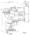
- FIG. 8 shows flow of the operations for processing a bitsteam.
- FIG. 9 shows a state machine implemented by decryptor 24 to evaluate key order.
- FIG. 10 a shows the structure of key memory 23 of FIG. 3 .
- FIG. 10 b shows the structure of the memory cells of FIG. 10 a.
- FIG. 11 shows the steps performed by control logic 23 a of FIG. 10 a to erase keys when made non-secure.
- FIG. 12 shows in more detail the battery supply switch of FIG. 10 a.
- FIGS. 13 and 14 show the level shift circuit and voltage detection circuit of the battery supply switch of FIG. 12 .
- FIG. 15 shows a state machine for erasing a design when a secure mode is exited.
- FIG. 16 shows a block diagram of elements for loading configuration memory and reading back configuration, including lines disabled when encryption is present.
- FIG. 1 shows a prior art structure for an FPGA 10 .
- the FPGA includes programmable logic 11 , typically comprising (1) logic blocks with lookup table combinatorial logic function generators, flip flops for storing lookup table outputs and other values, and multiplexers and logic gates for enhancing the logic ability of the programmable logic (2) routing lines and programmable interconnection points for routing signals around the FPGA, and (3) input/output blocks for driving signals between the routing lines and the external pins of the FPGA.
- the FPGA also includes configuration memory 12 for turning on routing transistors, controlling multiplexers, storing lookup tables and controlling the input/output blocks, all of this for the purpose of configuring the FPGA to perform the function desired by the designer(s).
- Bus 16 connects configuration memory 12 to programmable logic 11 and is typically a distributed set of control lines located throughout the FPGA.
- Some Xilinx products e.g. XC6200
- Such a structure is described by Kean in U.S. Pat. No. 5,705,938.
- FPGA 10 further includes a JTAG logic block 13 for interfacing with JTAG port 20 , especially intended for testing of the board in which the FPGA will be placed.
- JTAG logic block 13 implements the IEEE standard 1532, which is a superset of the IEEE standard 1149.1. JTAG allows debugging of a design at the board level.
- FPGA 10 includes configuration logic 14 for responding to a configuration bitstream from external source 15 on configuration access port 21 and for interfacing with JTAG logic block 13 .
- the bitstream on configuration access port 21 is treated as words, in one embodiment 32-bit words.
- Several of the words are used for setting up the configuration process and include, for example, length of a configuration memory frame, and starting address for the configuration data.
- Bus 19 allows communication between configuration logic 14 and JTAG logic block 13 so that the JTAG port can be used as another configuration access port.
- Bus 18 allows communication between configuration logic block 14 and configuration memory 12 . In particular, it carries addresses to select configuration frames in memory 12 , control signals to perform write and read operations, and data for loading into configuration memory 12 or reading back from configuration memory 12 .
- Configuration Logic block 14 receives instructions and data, and processes the data according to the instructions. These instructions come into configuration logic 14 as a bitstream. An instruction, or header, is usually followed by data to be acted upon. FIG. 2 a shows an example bitstream structure. Header A specifies an action and specifies that a single word, Data A, will follow. Header B specifies an action and in this case specifies that 4 words of data will follow to be acted upon.
- FIG. 2 b shows the default format (format type 001) for a 32-bit header word in the bitstream used in the Virtex® devices available from Xilinx, Inc. (Virtex is a registered trademark of Xilinx, Inc., assignee of the present invention).
- This format includes three bits to indicate the format type (001), two bits to specify an op code, 16 bits for a configuration logic register address, and 11 bits for a word count.
- the op code can designate a read operation, a write operation, or no operation. For example, 00 can designate no operation, 01 can designate read and 10 can designate write.
- the 11 bits for word count can specify 2 11 words or 2048 words. As shown in FIG.
- Format type 2 uses 27 bits to specify word count, and can thus specify 2 27 words or 2.68 million words.
- FIG. 2 d shows the kinds of control information that can be loaded into the registers of Configuration Logic 14 by headers for a Virtex bitstream.
- a header (of format 001) having the configuration logic register address 0000 specifies that the next 32-bit data word should be loaded into the cyclic redundancy check (CRC) register.
- CRC cyclic redundancy check
- the header includes an address 0001, the next data will be loaded into the Frame Address register in order to specify a frame (column) in configuration memory 12 to receive or provide data.
- the Configuration Logic Register address (16 bits) shown in FIG. 2 b provides the 4-bit values shown in the left column of FIG. 2 d that select one of the registers in configuration logic 14 ( FIG. 1 ) into which to place the next 32-bit data word.
- the Frame Length register (address 1011) specifies the length of the frame into which the configuration data will be loaded. (Frame length, or column height, depends upon the size of the PLD. Larger PLDs usually have taller columns or longer frames. Specifying the frame length in the bitstream and storing the frame length in a register rather than providing a different structure in the PLD for placing the data words into frames allows the internal configuration logic to be identical for PLDs of different sizes.)
- a read command is placed in the op code field and the Frame Data Output register is addressed, followed by a Word Count (using Command Header Format 2 if necessary).
- the specified number of words is read back from configuration memory 12 , starting at the address specified in the Frame Address register, and shifted out on either configuration access port 21 or JTAG port 20 . (Readback data is returned to the port that issued the readback instruction).
- Specifying a word count in a bitstream header or pair of headers sets a counter that counts down as the data words are loaded. For many configuration logic register addresses the word count is 1. But if the bitstream header has a configuration logic address of 0010 or 0011 to indicate configuration data are being loaded in or read back, the word count will be much larger. This is when header format 2 of FIG. 2 c is used. Data loaded into configuration memory 12 through the frame data input register (address 0010) or read out through the frame data output register (address 0011) is called the design data because it causes the FPGA to implement a design or shows the status of a design. The other register data are control data since they control how the configuration logic behaves while the logic is being configured or read back.
- Configuration logic 14 typically performs a cyclic redundancy check on a configuration bitstream coming in (see Erickson, U.S. Pat. No. 5,321,704 incorporated herein by reference, or see pages 39 through 40 of the above referenced Virtex Configuration Guide), reads header bits indicating the frame length of the part being configured and the word count of the configuration data, reads address instructions identifying where to load configuration data, collects frames of configuration data and loads them into columns of configuration memory 12 indicated in the addresses. Configuration logic 14 also controls readback of configuration data and flip flop values from configuration memory 12 to an external location. In a Virtex FPGA available from Xilinx, Inc., readback can be done through either JTAG port 20 or through configuration access port 21 .
- Configuration logic 14 can also receive configuration data from programmable logic 11 . More information about prior art FPGA structures in which part of the FPGA configures another part of the FPGA can be found in Kean, U.S. Pat. No. 5,705,938. More information about architectures of FPGAs similar to the Virtex architecture can be found in Young et al., U.S. Pat. No. 5,914,616. Both patents are incorporated herein by reference.
- FIG. 3 shows a block diagram of an FPGA (a type of PLD) according to one embodiment of the present invention. Some elements are the same as shown in FIG. 1 , are given the same reference numbers, and not explained again.
- FIG. 3 includes an expanded configuration logic unit 29 , a decryptor 24 and a key memory 23 .
- FIG. 3 shows an embodiment in which key memory 23 is loaded on bus 25 from JTAG access port 20 . In other embodiments, key memory 23 is loaded through another port.
- Bus 25 carries data, addresses, and control signals to perform write and read operations and allows programming of the decryption keys from JTAG port 20 .
- bus 26 allows programming of the keys from the configuration port. In another embodiment, bus 26 is eliminated.
- bus 26 is present and bus 25 is eliminated.
- bus 26 carries security data from key memory 23 to configuration logic 29 .
- bus 27 carries encrypted configuration data from configuration logic 29 to decryptor 24 and carries decrypted configuration data back to configuration logic 29 .
- Bus 28 allows decryptor 24 to access the keys for decrypting data.
- the bitstream comprises two portions, a data portion representing the user's design that can be encrypted or not, and a control portion controlling loading of the bitstream (for example giving addresses of columns in the PLD into which successive portions of the bitstream are to be loaded, providing a cyclic redundancy check (CRC) code for checking reliability of the loading operation, and a starter number for cipher block chaining (CBC), a technique that prevents a “dictionary attack” where the decrypted data can be deduced from the frequency of occurrence of the encrypted data).
- the data portion may be encrypted but the control portion is unencrypted.
- the address of the configuration data is also encrypted, but other control information in the configuration bitstream remains unencrypted.
- FIGS. 4 a – 4 d illustrate differences in bitstream format and registers of configuration logic 29 in comparison to the format and registers of configuration logic 14 of the prior art product shown in FIGS. 2 a – 2 d .
- the bitstream still includes header words followed by data words.
- FIG. 4 a shows an example in which three header words Header A, Header B, and Header C are each followed by three unencrypted control data words Data A, Data B, and Data C.
- Header D specifies that encrypted configuration data will follow and is followed by multiple words Data 1D, Data 2D, Data 3D, etc. of encrypted configuration data. These words have been shaded in FIG. 4 a to emphasize that this data is encrypted.
- a fourth op code has been added.
- the new value 11 specifies that writing is to be with decryption. (It is not important what code or what method is used to specify that decryption is to be used or even that it is specified through an op code. It is just important that optional encryption and decryption be allowed and indicated, so that designers can make use of this option.
- FIG. 4 d two new configuration logic registers are added. Shown at addresses 1100 and 1101 are the register for holding a cipher block chaining (CBC) starter value and the address for the initial encryption key.
- CBC cipher block chaining
- a PLD can accept both encrypted and unencrypted data portions of the bitstream.
- the control portion of the bitstream indicates whether the data portion of the bitstream is encrypted. If the data portion of the bitstream is encrypted, it is diverted within the PLD to a decryptor and after decryption is used to configure the PLD. If unencrypted, it is not diverted, and is used directly to configure the PLD.
- FIGS. 5 a and 5 b show example bitstream portions representing the same design, first unencrypted and then encrypted, to illustrate the differences between an unencrypted bitstream and an encrypted bitstream in one embodiment of the invention.
- An actual bitstream includes the 0's and 1's at the right of the figures and none of the text at the left. The text at the left is provided to explain the meaning of the bits to the right.
- These bitstream portions use the commands illustrated in FIGS. 4 b – 4 d .
- the differences are shown in bold.
- FIG. 5 a after a dummy word (a constant high signal interpreted as all 1's) and a sync word with a specified pattern of 1's and 0's, the next word is of type 001 with an op code of 10, has an address of 0000000000010000 and a word count of 00000000001. Thus this word addresses the command register CMD and specifies that one word will be written there.
- FIG. 5 a has been annotated to the left of the bitstream to indicate that this word is Type 1 and indicates to write 1 word to CMD.
- the following word 111 is the data to be placed in command register CMD, and resets a CRC (cyclic redundancy check) register.
- CRC cyclic redundancy check
- the PLD includes a circuit, not shown, such as described by Erickson in U.S. Pat. No. 5,598,424 to calculate a CRC value from the bitstream as the bitstream is being loaded, and protects against glitches in the bitstream voltages that might cause incorrect bits to be loaded.
- a header word specifies that the format is again type 1 and it specifies to write 1 word to the frame length register FLR.
- the data word that follows, 11001 specifies the frame length (25 words).
- several additional header and data words follow, including the header specifying the word to be written to the frame address register FAR. In this case, the following data word indicates data will start at address 0.
- FIG. 5 b is similar to FIG. 5 a , and differs only where the data and annotations are shown in bold.
- the data are encrypted, and additional commands are used to provide the initial key address and to write two words (64 bits) to the CBC (cipher block chaining) register.
- a type 1 header includes the op code 11 and indicates that data will be decrypted before being written to frame data input register FDRI.
- a type 2 header follows, again with the op code 11 , giving the instruction that 10530 words are to be decrypted and written to data input register FDRI.
- the 10530 encrypted data words then follow.
- the CRC word follows for confirming that the (encrypted) data were loaded correctly.
- the additional commands and data are sent, and place the PLD into operation mode if all is correct.
- FIG. 6 shows how optional decryption is accomplished in one embodiment.
- FIG. 6 shows the detail of configuration logic 29 and of buses 27 and 28 leading into decryptor 24 .
- Bus 27 includes the following:
- One potential attack on a design in an encrypted bitstream is to change the frame address register (starting address) in the encrypted bitstream so that when it is decrypted it is loaded into a portion of the FPGA visible when the FPGA is being used.
- the content of the block RAM is visible.
- the configuration of the input/output ports is visible and therefore the configuration bits can be determined.
- FIGS. 7 a and 7 b show the encryption and decryption portions of a triple DES algorithm, respectively, as modified according to the invention.
- the standard cipher block chaining method starts the encryption process by XORing a starting number (can be designer supplied or randomly generated) with the first word of data to be encrypted. According to the invention, part of the random number is replaced by address information, in the present example the 22-bit address of the first frame into which data will be loaded in configuration memory 12 .
- the starter CBC value a 64-bit number, has its least significant bits, labeled x, replaced by the frame address, labeled y, to produce a modified 64-bit value that depends upon the address into which data will be loaded.
- This modified CBC value is XORed with the first word of configuration information Word1.
- the encryption algorithm is used to produce the first encrypted word Encrypted Word1, which is placed into the bitstream.
- FIG. 7 a shows a triple encryption algorithm with outer cipher block chaining, comprising an encryption step enc 1 using the first key, followed by a decryption step dec 2 using the second key, followed by an encryption step enc 3 using the third key.
- This first encrypted word Encrypted Word1 is XORed with the second unencrypted word Word2 and the encryption process is repeated to produce encrypted Word2.
- the XOR chaining continues until all configuration data have been encrypted.
- the PLD must perform the reverse process to derive the decrypted words.
- the decryption sequence would be decryption step dec 1 using key 3, then encryption step enc 2 using key 2, then decryption step dec 3 using key 1.
- part of the initial value for generating Decrypted Word1 is to use the same frame address for both encryption and decryption.
- the PLD not the bitstream, generates the modified CBC value from the frame address stored in the frame address register, which is also used to specify the frame of configuration memory 12 into which configuration data are to be loaded. So if an attacker changes the frame address into which the data are to be loaded, the modified CBC value changes accordingly, and the configuration data are not correctly decrypted.
- the XOR step produces the original data that was in the designer's bitstream before it was encrypted.
- Original Word1 Decrypted Word1, for example.
- This decrypted configuration data is sent on bus 27 ( FIG. 3 ) to configuration logic 29 .
- Configuration logic 29 includes the structures to support optional encryption as well as the structures to prevent design relocation and a single key attack. As shown in FIG. 6 , configuration logic 29 includes a holding register 292 , control logic 291 , configuration registers (FDRI, FAR, CRC, and init CBC are shown), decryptor 24 interface multiplexers 294 and 295 , 64-bit assembly register 297 , and registers 298 and 299 (for interfacing with configuration access port 21 ). A 64-bit shift register 299 receives data from configuration access port 21 , which can be a single pin for 1-bit wide data or 8 pins for 8-bit wide data. This data is loaded into 64-bit shift register 299 until register 299 is full.
- multiplexer 296 b alternately selects right and left 32-bit words, and multiplexer 296 a moves the data 32 bits at a time either into holding register 292 or alternately into High and Low portions of assembly register 297 as controlled by control line M.
- line M and a clock signal not shown cause multiplexers 296 a and 296 b to move data from 64-bit transfer register 298 to holding register 292 . From there these words are applied to control logic 291 . If the word is a header, control logic 291 interprets the word.
- control logic 291 places an address on bus G to select a register, places a signal on line L to cause multiplexer 294 to connect bus B to bus D, and applies the following word on bus B. On the next clock signal (clock signals are not shown), the data on bus D are loaded into the addressed register. All registers shown in FIG. 4 d can be loaded this way.
- the init CBC register for loading the initial cipher block chaining value is a 64-bit register and receives two consecutive 32-bit words, as shown in FIG. 5 b and discussed above.
- a modified CBC value formed from (1) the original CBC value stored in the init CBC register and (2) the initial frame address stored in the FAR register is available to decryptor 24 .
- the initial frame address in the FAR register uses no more than 32 bits while the init CBC value uses 64 bits.
- the 64-bit bus providing the modified CBC value includes 22 bits from the frame address register FAR and 42 bits from the init CBC register. Important to the security provided by the present invention, note that this value depends upon where configuration data will be loaded. If an attacker were to try to load encrypted data into a different place by changing the contents of the FAR register, the modCBC value fed to decryptor 24 would also change.
- Control line M causes multiplexer 296 a to apply data from transfer register 298 to bus A leading to assembly register 297 .
- Control bus H alternately connects bus A to the High[31:0] and Low[31:01] portions of encrypted data register 297 to form a 64-bit word to be decrypted.
- Control logic 291 then asserts the Enc — data — rdy signal, which causes decryptor 24 to decrypt the data in register 297 .
- decryptor 24 applies a key address KeyAddr on bus 28 to key memory 23 ( FIG. 3 ). This causes key memory 23 to return the 56-bit key in that address on the 56-bit Key lines. It also causes key memory 23 to return two additional bits “Order” also stored in the key data at that address. For the first decryption key, these two bits must indicate that this is a first key or an only key. If not, decryptor 24 asserts the Bad — key — set signal, which causes control logic 29 to abort the configuration operation. If these two bits indicate the key is a first or only key, decryptor 24 performs the decryption, using for example the well known DES algorithm (described by Schneier, ibid).
- decryptor 24 then gets the key at the next address in key memory 23 , and checks to see if the two Order bits indicate it is a middle or last key. If not, the Bad — key — set signal is asserted and the configuration is aborted. If so, decryption is performed. If it is a middle key, another round of decryption is done. If it is the last key, decryptor 24 forms the XOR function of the decrypted word and the value modCBC. Decryptor 24 then places the resultant value on the 64-bit Decrypted — data bus and asserts the Dec — data — rdy signal.
- control logic 291 This causes control logic 291 to place signals on control line K to cause multiplexer 295 to break the 64-bit word into two sequential 32-bit words.
- Control logic 291 places a signal on line L to cause multiplexer 294 to forward the 32-bit words of decrypted data to bus D.
- Control logic 291 also places address signals on bus G to address frame data input register FDRI. The next clock signal moves the decrypted data to bus E where it is loaded into the frame register and when the frame register is full, eventually shifted into configuration memory 12 at the address indicated in the FAR register.
- the modCBC value is used only once in the decryption operation. Subsequent 64-bit words of encrypted data are decrypted and then chained using the previously decrypted data for the XOR operation. (The value stored in the FAR register is also used only once to select a frame address. Subsequently, the frame address is simply incremented every time a frame is filled.)
- FIG. 8 indicates the flow of operations performed by configuration logic 29 and decryptor 24 .
- Configuration logic 29 begins at step 70 by loading the bitstream headers and placing the corresponding data into configuration logic registers shown in FIG. 4 b , including determining bitstream length.
- configuration logic 29 reads the first configuration memory address. Recall that the bitstream format includes an op code that indicates whether encryption is being used. Step 72 branches on the op code value. If encryption is not used, the process is shown on the left portion of FIG. 8 . If encryption is used, the process is shown in the right of FIG. 8 . For no encryption, at step 73 , configuration logic 29 sets a counter equal to the bitstream word count (see FIG.
- step 74 32 bits (1 word) of configuration data are sent to the addressed frame of configuration memory 12 . If step 75 indicates the counter is not finished, then at step 76 the counter is decremented and the next 1 word of configuration data are sent to configuration memory 12 . When the counter has finished, configuration logic 29 performs cleanup activities including reading the final cyclic redundancy value to compare with a value at the end of the bitstream to determine whether there were any errors in loading the bitstream.
- step 72 indicates the bitstream is encrypted
- the counter is loaded with the word count, and at step 81 the process loads the initial key address from key address register 293 ( FIG. 6 ) into decryptor 24 .
- two words (64 bits) of encrypted configuration data are loaded into decryptor 24 .
- the addressed key is loaded into decryptor 24 .
- a 64-bit number is loaded into decryptor 24 .
- This 64-bit number includes a 56-bit key, two bits that indicate whether it is the first, middle, last, or only key, and some other bits that may be unused, used for parity, or used for another purpose.
- the 64-bit key data includes a single bit that indicates whether it is or is not the last key.
- the 64-bit key data includes an address for the next key so the keys don't need to be used in sequential order.
- extra bits are not present and the key data uses less than 64 bits.
- bitstream rather than the key indicates how many keys are to be used, but this is believed to be less secure because an attacker can see how many keys are used and perform a single key attack, breaking one key at a time, whereas using the keys to indicate how many keys are to be used does not give this information to an attacker.
- decryptor 24 decrypts the 64-bit data with the 56-bit key using, for example, the DES algorithm.
- the DES algorithm is described in the above-mentioned book by Bruce Schneier at pages 265 to 278.
- Other encryption algorithms may also be used, for example, the advanced encryption standard AES.
- Other algorithms may require more key bits. For example AES requires a key of 128 to 256 bits.
- Step 85 determines whether more keys are to be used. The two bits that indicate whether the key is first, middle, last, or only key are examined to determine whether this is the last key, and if not, the key address is incremented and decryptor 24 addresses the next key in memory 23 .
- the modified CBC value shown in FIG. 6 as a 64-bit value from combining registers FAR and init CBC is XORed with the decrypted value obtained in step 87 .
- 22 bits of the 64-bit random number loaded into the CBC register are replaced with the frame address of the beginning of the bitstream.
- the goal of the encryption process is to have every digit of the 64-bit encrypted value be a function of all previous bits plus the key.
- the goal of combining the CBC value with the first address is to cause the decrypted values to change if the bitstream is loaded into a different address from the intended starting address.
- Step 87 achieves both goals.
- the new CBC value is then stored. Storage may be in the FAR and init CBC registers shown in FIG. 6 , or in another register located in decryptor 24 .
- this decrypted configuration data is sent on bus 27 ( FIG. 3 ) to configuration logic 29 .
- Configuration logic 29 calculates an updated cyclic redundancy check value to be compared with the cyclic redundancy value stored in the CRC register at the end of the loading process. If configuration logic 29 has been set to use encryption, a multiplexer in configuration logic 29 forwards this decrypted configuration data to the addressed column of configuration memory 12 .
- step 89 the counter is checked and if not finished, at step 96 the counter is decremented and the process returns to step 82 where the next 64 bits (2 words) are loaded from the bitstream.
- step 90 a CRC (cyclic redundancy check) value in the bitstream is compared with a CRC value calculated as the bitstream is loaded. If the values agree, configuration is complete and the FPGA goes into operation. If the values do not agree, a loading error has occurred and the entire configuration process is aborted.
- CRC cyclic redundancy check
- FIG. 9 shows a state machine implemented by decryptor 24 to evaluate key order.
- the state machine remains in state S 1 until the Enc — data — ready signal is activated. This signal indicates decryption can begin and moves to decision state Q 1 where decryptor 24 applies the address specified by the address Init — key — addr on bus 27 to bus 28 , reads back a key and a key order, and from the two bits of key order data determines whether the key is a first or only key. If not, decryptor 24 sends the Bad — key — set signal to control logic 291 and causes configuration logic 29 to abort the configuration. If the address is first or only, decryptor 24 goes to state S 3 , which decrypts the data.
- state machine goes to decision state Q 2 , which determines whether the key is last or only. If so, decryption is complete and at state S 4 decryptor 24 returns the decrypted data to configuration logic 29 . If not, in state S 5 , decryptor 24 increments the key address, and gets the new key. The state machine asks question Q 3 to determine whether the next key is a middle or last key. If not, state S 2 causes the configuration to abort. If the key is middle or last, the state machine returns to state S 3 to decrypt the data again. In another embodiment, in state S 4 decryptor 24 also performs the step of XORing the decrypted data with a CBC value.
- the benefit of storing the key order within the keys is that an attacker can not implement a single key attack because the attacker can not prevent decryptor 24 from using all the keys specified by key memory 23 (as intended by the designer) when performing decryption. It is not necessary to ask the second and third questions Q 2 and Q 3 to protect against an attacker using a single key attack, since the key order is stored within the key data inside the PLD. However, it is beneficial to the designer or board tester who loads the keys to ask all three questions to make sure that each key has been labeled correctly when it is loaded.
- decryptor 24 uses the triple DES standard with a decryption-encryption-decryption sequence, alternating the algorithm (only slightly) each time another key is used. Such a combination is in accordance with the ANSI X9.52 1998 Triple DES standard. In another embodiment, decryption is used each time.
- the circuit shown in FIG. 10 a includes three components: battery supply switch 22 , control logic 23 a and key registers 23 b .
- Control logic circuit 23 a and key registers 23 b comprise key memory 23 of FIG. 3 .
- key registers 23 b comprise six 64-bit words. Of course, other key memory sizes may alternatively be used. In other embodiments, there may be far more than six keys stored in key memory 23 , and more than 3 bits needed to give the address of the key to be used.
- the power supply for key registers 23 b comes from battery supply switch 22 on line VSWITCH. When key memory supply voltage VCCI is insufficient or not present, battery supply switch 22 applies the battery backup voltage VBATT to the VSWITCH line so that VSWITCH carries a positive voltage.
- each key register has 64 memory cells.
- Each cell receives a write enable signal WE, that when high causes data to be written to the cell and when low causes data in the cell to be held.
- Cells in one register have a common write enable signal WE.
- weak pull-down transistors such as T 1 pull down the WE signal so that none of the key memory registers can be addressed, and none of the memory cells are disturbed.
- the JTAG port of a PLD is used to load decryption keys into the PLD.
- the memory cell supply voltage is at the device voltage level of VCCI during normal operation, and in one embodiment this level is between 3.0 and 3.6 volts.
- Signals applied to the JTAG port may be several different voltages. Also, there may be several different internal voltages. Thus voltage translation is needed. This voltage translation is performed in the memory cells. Detail of a memory cell is shown in FIG. 10 b .
- the latch comprising inverters I 1 and I 2 is powered by VSWITCH and is thus powered whether or not a device supply voltage VCCI is present.
- the WE signal and the inverted data signal data — b both operate at the 1.5 volt level.
- FIG. 10 b shows that when WE is low, transistors T 4 and T 5 are off, and the content of the latch comprising inverters I 1 and I 2 is retained. When WE is high, one of inverters I 1 and I 2 is pulled low, thus loading the new data into the latch.
- Control logic circuit 23 a receives signals from JTAG bus 25 (also shown in FIG. 3 ).
- JTAG bus 25 includes control signals for writing, reading, setting the secure mode, and data and address buses. This interface conforms to the IEEE 1532 JTAG standard.
- the security status (bus 26 ) is placed in non-secure mode, which can be done using the ISC — PROGRAM — SECURITY instruction (see FIG. 10 a ) and applying logic 1 to bit 0 of the key data bus.
- Key memory 23 is written to and read (for verification) from JTAG bus 25 using the ISC — PROGRAM and ISC — READ instructions of the IEEE 1532 standard.
- Control logic 23 a includes a decoder for decoding the 3-bit address signal ADDR from JTAG bus 25 to produce a low-going pulse on the addressed one of write strobe lines ws — b[5:0] if the ISC — PROGRAM instruction appears on JTAG bus 25 , or a high signal on the addressed one of read select lines rsel[5:0] if the ISC — READ instruction appears on JTAG bus 25 .
- One of the six 64-bit words can be read by applying a high signal to one of the six read select lines rsel[5:0], which causes read multiplexer 23 d to place the selected word on the 64 output lines q[63:0]. Only one of the write select lines or read select lines is selected at one time. When no read select signal is asserted, a high park low signal causes 64 transistors 23 e to pull down the 64 lines q[63:0] and prevent these lines from floating.
- the 64-bit words can be read from key registers 23 b to JTAG bus 25 where the values can be examined external to the FPGA.
- the FPGA can be tested in this non-secure mode by using 56 bits of a selected 64-bit word in registers 23 b as the 56-bit key for DES decryption.
- key memory 23 is in non-secure mode, readback of a user's design is possible even though the design has been encrypted before loading. This allows the designer to test and debug even an encrypted design. Communication of the key security status is through bus 26 (see also FIG. 3 ).
- control logic 23 a After values have been written into key registers 23 b and verified with a read operation from bus 25 , control logic 23 a is placed into secure mode by using the ISC — PROGRAM — SECURITY instruction and applying logic 0 to bit 0 of the 64-bit key data bus which is part of the IEEE 1532 standard. In the secure mode, no access to the keys is granted.
- a state machine in control logic 23 a erases all keys by writing zeros to all six words, one word at a time.
- step 110 putting zeros on the wdata[63:0] bus and at step 111 asserting the ws — b[0] signal (with a logic 0 value), then at steps 112 – 117 successively strobing the ws — b[0:0] through ws — b[5:0] signals one at a time before changing the security status at step 118 and entering the non-secure mode, and finally at step 119 releasing the wdata[63:0] logic 0 values.
- any attempt to place battery backed up memory 23 into a non-secure mode causes all values in key registers 23 b to be erased.
- control logic 23 a sends a secure mode signal on bus 26 (may be a single line) to configuration logic 29 to indicate that key memory 23 is operating in secure mode. If this signal switches to non-secure mode, configuration logic 29 clears the design from configuration memory 12 . Note that an unencrypted bitstream may be loaded by configuration logic 29 into configuration memory 12 even though keys are stored in key registers 23 b and key memory 23 is in a secure mode.
- Decryption keys must be loaded into the PLD before the PLD is put into a secure mode where a user can not learn details of the design.
- the key or keys are loaded through a JTAG port 20 .
- the encryption keys are loaded through this JTAG port 20 . It is expected that JTAG programmers will load the encryption keys during board testing.
- the RAM for storing keys is in a non-secure mode, the user has full access to it and can read out both the keys and the design, even if the design has been encrypted. This is useful for the designer while testing the keys and the use of the keys. Then once the designer is satisfied with the operation, he or she can send another instruction through the JTAG port and place the key memory into a secure mode. Once the key memory has been placed into secure mode, the keys can not be read out. Further, moving the key memory from secure to non-secure mode erases the keys by activating a circuit that starts up the memory initialization process. ( FIG. 15 , discussed below, shows a state machine for performing this function.)
- more than one key may be used to encrypt the design. For example, if three keys are to be used, the bitstream is first encrypted using the first key, then the resulting encrypted bitstream is again encrypted using the second key, then finally the resulting doubly encrypted bitstream is again encrypted using the third key.
- This triply encrypted bitstream is stored, for example in a PROM or flash memory on the printed circuit board that holds the PLD.
- these keys are used in succession (reverse order) to repeatedly decrypt the encrypted bitstream.
- the encrypted bitstream may include in an unencrypted portion an indication of how many keys are to be used, and the address of the first key.
- the keys themselves may indicate whether they are the first, middle, last, or only keys.
- the same PLD can at different times be programmed to perform different functions (configured with different designs), and information about the values of the different keys can be made available to only one or some of the designers.
- a first designer may not learn about a second design even though both designs are implemented in the same PLD (at different times).
- configuration logic 29 includes additional logic beyond configuration logic 14 of FIG. 1 .
- the bitstream on configuration access port 21 is treated as words, in one embodiment 32-bit words.
- Several of the words usually at or near the beginning of the bitstream, contain header information, for example length of the bitstream, starting address for the configuration data.
- New to the bitstream of the present invention is an indication as to whether the bitstream is encrypted, and the address of a key for decrypting configuration data in the bitstream.
- Values stored in key memory 23 are preferably retained by a battery when power to the FPGA is removed.
- a PLD can be manufactured in which the VSWITCH voltage supply is routed to all flip flops in the PLD if the purpose is to preserve data generated by the PLD when the PLD is powered down. And if the purpose is to also preserve configuration of the PLD when the PLD is powered down, configuration memory 12 ( FIG. 3 ) may alternatively be powered from VSWITCH, though such an embodiment requires considerably more battery power than does powering just the flip flops in the PLD, and powering flip flops in turn requires more battery power than does powering a very small memory for storing a few encryption keys.
- FIG. 12 shows a structure for battery supply switch 22 .
- VBATT level shift circuit 31 allows the PLD to use different voltages for the battery and main power supply. And of course the purpose of the circuit is to deal with varying voltage levels.
- battery supply switch 22 can handle VCCI voltages up to 3.6 volts, and switches to battery power when VCCI falls below about 1 volt. Battery voltage can be between 1.0 volts and 3.6 volts.
- Battery supply switch 22 includes four output driving P-channel transistors P 0 through P 3 .
- Transistors P 0 and P 1 turn on and off together as do transistors P 2 and P 3 .
- the circuit includes two transistors for each leg instead of one in order to avoid any possibility that VCCI and VBATT will be connected together.
- Transistor P 0 includes a parasitic diode (the p-n junction between the drain and substrate) that can conduct current upward in the figure even when the transistor is off. To prevent such current flow, transistor P 1 is added and has its substrate connected to its drain so that parasitic diode conduction can only be downward. A similar arrangement is made with transistors P 2 and P 3 .
- Transistor P 4 is a resistor, always on, and provides protection against electrostatic discharge. Most of the time, the structures controlled through transistor P 4 do not draw current, so there is usually no voltage drop across transistor P 4 .
- FIG. 13 shows one embodiment of VBATT level shift circuit 31 .
- Output voltage at terminal OUT is controlled by signals IN and INB. These signals are generated by inverters 33 and 34 , which derive their supply voltage from the VSWITCH node. Therefore, if VSWITCH is supplied by VBATT, one of signals IN and INB will be at voltage VBATT and the other will be at ground. However, if VSWITCH is supplied by VCCI, one of IN and INB will be at the VCCI voltage level. If IN is at VCCI and INB is at ground, transistor 45 will be on and transistor 46 will be off. The gate of P-channel transistor 43 will be low, and transistor 43 will be on, pulling the input of inverter 47 to VBATT. The output of transistor 48 will also be at VBATT. Returning to FIG. 12 , a voltage level VBATT at the gate of transistor P 0 will positively turn off transistor P 0 .
- FIG. 14 shows VCCI detect circuit 32 .
- VCCI detect circuit 32 determines when the voltage on line VSWITCH will be switched to the battery and back to VCCI.
- This embodiment of circuit 32 is essentially a string of five inverter stages I 1 through I 5 . Controlling of the switching voltage occurs primarily at inverter stage I 1 .
- Transistors 52 and 53 form a CMOS inverter. Power to this CMOS inverter must flow through P-channel transistor 51 , which doesn't turn on until VCCI reaches the threshold voltage of transistor 51 , typically 0.7–0.8 volts. If VCCI is switching slowly, taking several milliseconds to reach full voltage, transistor 51 delays the activation of circuit I 1 .
- N-channel transistor 53 typically has a threshold voltage of about 0.7–0.8 volts as well but is sized as a weak transistor relative to transistor 52 .
- transistor 53 has a width/length ratio of 1/18 whereas transistor 52 has a width/length ratio of 3/2. So transistor 53 pulls the input of inverter I 2 low only until transistor 52 turns on.
- circuit I 1 pulls the input of inverter stage I 2 high when VCCI is at about 1.0 volt. Thus the output of inverter 54 goes low.
- Inverter stage I 3 is a Schmitt trigger.
- inverter stage I 3 The zero volt input to inverter stage I 3 turns off transistors 56 and 57 and turns on transistor 55 , pulling node N 3 to VCCI and turning on transistor 58 , which pulls up node N 4 , thus raising the voltage at which transistor 56 will turn on, and preventing small variations in VCCI from switching the voltage at node N 3 .
- Inverters 59 and 60 are optional and produce a sharper edge of the output signals usebatt and usebattb that cause battery supply switch 22 of FIG. 12 to switch from VBATT to VCCI.
- Transistor 61 controlled by the VBATT′ signal, is a weak pull-down transistor and assures that the usebattb line is pulled low when VCCI is not present and therefore not providing an output signal from inverter 60 .
- a key is loaded into the PLD before sale of a system incorporating the PLD, such that after sale of a system including the PLD, the design can be loaded into the PLD and used, but an attacker can not learn the value stored in the key (or keys). Thus the unencrypted design can not be read or copied. To achieve this security, several steps are taken.
- FIG. 15 shows a state machine for performing the design clearing function.
- the state machine enters state S 1 .
- This state monitors a change from secure to non-secure mode of the secure — design flag. As long as the secure-design mode continues, the state machine stays in state S 1 .
- the state machine enters state S 2 and the data shift registers for shifting data into configuration memory 12 are reset, thereby placing zeroes on all data lines for the configuration memory bits.
- the state machine moves to state S 3 where the word line of the addressed frame is asserted. This results in the zeros on the data shift register lines being written into the memory bits at the addressed frame.
- question Q 1 indicates there are more frames to be addressed, the state machine moves to state S 4 where the frame address is advanced and the state machine returns to state S 3 .
- question Q 1 indicates there are no more frames to be addressed, the process is done and the configuration memory is cleared.
- the key loading process begins in a non-secure mode by clearing all key registers.
- a secure key flag must be kept in the non-secure mode while keys are loaded and while the keys are read back for verification.
- the secure key flag may also be kept in the non-secure mode while a configuration bitstream is loaded and decrypted. But once the secure key flag is set, returning the secure key flag to the non-secure mode clears all keys and also initiates operation of the state machine of FIG. 15 . So, not only are the keys cleared, but the configuration is also cleared.
- Some FPGAs allow a bitstream to be read back out of the FPGA so that a user may debug a design or may obtain state machine information from flip flops in the FPGA. Unless the design were re-encrypted for the read-back operation, the act of reading back the bitstream would expose the unencrypted bitstream to view.
- readback is disabled only if the decryption keys are also secured.
- FIG. 16 shows the block diagram of a structure for loading and reading back configuration memory.
- configuration logic 29 prevents readback when two conditions are present: (1) the security status line on data bus 26 (see FIGS. 3 and 10 ) indicates that the keys are in a secure mode, and (2) configuration logic 29 has responded to op codes in a configuration bitstream that indicate the bitstream is encrypted. So if either the keys are not secured or the bitstream is not encrypted, readback can be enabled. In other embodiments, different conditions control whether readback can be enabled.
- configuration logic 29 When configuration logic 29 receives in the bitstream a header indicating that readback is to be performed, it sends on line 107 the frame address stored in its frame address register, which is decoded by address decoder 110 to select the addressed line of bus 109 . Next, word line enable signal on line 108 is asserted, which asserts the selected word line of bus 109 to allow memory cells addressed by the selected word line to place their values on the n data lines 102 (n is the frame length and is stored in configuration logic 29 ). Configuration logic 29 then asserts the Load signal on line 104 to load the frame of data (in parallel) into data shift register 101 .
- configuration logic 29 asserts the shift signal on line 105 to cause data shift register 101 to shift out the frame of data in 32-bit words on bus 103 to the frame data output register (see FIG. 4 d ) and from there to an outgoing bitstream on configuration access port 21 ( FIG. 3 ).
- configuration logic 29 sets internal flags to indicate this. If these flags are set and key memory 23 is in secure mode as indicated by the security status signal on bus 26 , then configuration logic 29 responds to a readback command in the bitstream by keeping the word line enable signal on line 108 inactive and by keeping the load and shift signals on lines 104 and 105 inactive to prevent readback. However, if key memory 23 is not in secure mode, even though the design may be encrypted, readback is allowed so that testing and debugging are possible.
- Some FPGAs allow partial reconfiguration of the FPGA or allow different parts of a design to be loaded into different parts of the FPGA using separate starting addresses and separate write instructions.
- An attacker might attempt to learn the design by partially reconfiguring the design to read contents of a block RAM or flip flops directly to output ports or by adding a section to an existing design to read out information that can be used to learn the design. For example, the attacker might partially reconfigure the PLD with an unencrypted design whose only purpose is to extract information about the encrypted design.
- Such a Trojan Horse design could be loaded into the PLD with another bitstream or attached to an existing encrypted bitstream. If the attacker was interested in learning a state machine design loaded into block RAM of an FPGA, for example, the Trojan Horse design could include logic to cycle through the addresses of the block RAM and send the block RAM data contents to package pins.
- configuration logic 29 disallows partial reconfiguration once configuration with decryption is started. Configuration logic 29 disallows a further write instruction once a header with the decryption op code has been processed. Also, configuration logic 29 disallows configuration with decryption once configuration without encryption has been done. Configuration logic 29 accomplishes these restrictions by ignoring headers that write to configuration memory after a decrypt instruction has been received and ignoring headers that have a decrypt command if an unencrypted portion of a design has been loaded. Thus, if any op code indicates that writing with decryption is being used, the PLD will accept only a single write instruction.
- the starting address and the design data are both encrypted. In this embodiment, it is possible to load several segments of encrypted design data starting at different frame addresses, just as is possible with unencrypted design data.
- the key data stored in a key memory such as key memory 23 specifies the number of keys that will follow.
- the key data also specify the number of keys that precede the key. If an attacker gives a key address other than the first key address intended by the designer, the configuration may be aborted. Additionally, encryption will proceed until the number of keys specified within the keys have been used.
- the keys instead of allowing keys to be read back when the key memory is in a non-secure mode, the keys include parity bits or CRC check bits, and only these bits can be read back for verification that the key or keys were loaded correctly.
- This embodiment allows keys known to one designer to be kept secret from another designer, and is useful when the PLD is to be used at different times for loading different designs.
- embodiments can be provided in which the CRC checksum is calculated either before or after a design is encrypted.
- the checksum added to the bitstream is calculated before the design data is encrypted, then a corresponding checksum must be calculated within the PLD on the design data after it has been decrypted.
- the checksum added to the bitstream is calculated after the design data has been encrypted, then the PLD must calculate the corresponding checksum on the received bitstream before the design data have been decrypted.
Abstract
To prevent copying of a design implemented in a programmable logic device (PLD), the PLD itself stores a decryption key or keys loaded by the designer, and includes a decryptor for decrypting an encrypted configuration bitstream as it is loaded into the PLD. The PLD also includes logic for reading header information that indicates whether the bitstream is encrypted, and can accept both encrypted and unencrypted bitstreams. The encryption keys may be stored in non-volatile memory or backed up with a battery so that they are retained when power is removed.
Description
The invention relates to PLDs, more particularly to protection of designs loaded into a PLD through a bitstream.
A PLD (programmable logic device) is an integrated circuit structure that performs digital logic functions selected by a designer. PLDs include logic blocks and interconnect lines and typically both the logic blocks and interconnections are programmable. One common type of PLD is an FPGA (field programmable logic device), in which the logic blocks typically include lookup tables and flip flops, and can typically generate and store any function of their input signals. Another type is the CPLD (complex programmable logic device) in which the logic blocks perform the AND function and the OR function and the selection of input signals is programmable.
Problem with Storing Bitstream External to PLD
Designs implemented in PLDs have become complex, and it often takes months to complete and debug a design to be implemented in a PLD. When the design is going into a system of which the PLD is a part and is to be sold for profit, the designer does not want the result of this design effort to be copied by someone else. The designer often wants to keep the design a trade secret. Many PLDs, particularly FPGAs, use volatile configuration memory that must be loaded from an external device such as a PROM every time the PLD is powered up. Since configuration data is stored external to the PLD and must be transmitted through a configuration access port, the privacy of the design can easily be violated by an attacker who monitors the data on the configuration access port, e.g. by putting probes on board traces.
Current Solutions and their Disadvantages
Efforts have been made to encrypt designs, but it is difficult to make the design both secure from attackers and easy to use by legitimate users. The encryption algorithm is not a problem. Several encryption algorithms, for example, the standard Data Encryption Standard (DES) and the more secure Advanced Encryption Standard (AES) algorithm, are known for encrypting blocks of data. The process of cipher block chaining (CBC), in which an unencrypted data word is XORed with the next encrypted data word before decryption allows the DES or AES to encrypt a serial stream of data and these are therefore appropriate for encrypting a bitstream for configuring a PLD. A key used for encrypting the design must somehow be communicated in a secure way between the PLD and the structure that decrypts the design, so the design can be decrypted by the PLD before being used to configure the PLD. Then, once the PLD has been configured using the unencrypted design, the design must continue to be protected from unauthorized discovery.
A Nov. 24, 1997 publication by Peter Alfke of Xilinx, Inc. entitled “Configuration Issues: Power-up, Volatility, Security, Battery Back-up” describes several steps that can be taken to protect a design in an existing FPGA device having no particular architectural features within the FPGA to protect the design. Loading design configuration data into the FPGA and then removing the source of the configuration data but using a battery to maintain continuous power to the FPGA while holding the FPGA in a standby non-operational mode is one method. However, power requirements on the battery make this method impractical for large FPGA devices.
Nonvolatile configuration memory is another possibility. If the design is loaded at the factory before the device is sold, it is difficult for a purchaser of the configured PLD device to determine what the design is. However, a reverse engineering process in which the programmed device is decapped, metal layers are removed, and the nonvolatile memory cells are chemically treated can expose which memory cells have been charged and thus can allow an attacker to learn the design. Further, nonvolatile memory requires a more complex and more expensive process technology than standard CMOS process technology, and takes longer to bring to market.
It is also known to store a decryption key in nonvolatile memory in a PLD, load an encrypted bitstream into the PLD and decrypt the bitstream using the key within the PLD. This prevents an attacker from reading the bitstream as it is being loaded into the PLD, and does retain the key when power is removed from the PLD. Such an arrangement is described by Austin in U.S. Pat. No. 5,388,157. But this structure does not protect the user's design from all modes of attack.
In addition to design protection, some users need data protection. They may have generated data within the PLD that should not be lost when the PLD loses power. It is desirable to protect such data.
There remains a need for a design protection method that is convenient, reliable, and secure.
The invention provides several structures and methods for protecting a PLD from unauthorized use and data loss.
If the PLD is configured by static RAM memory that must be loaded on power-up, the configuration data must be protected as it is being loaded into the device. As in the prior art, this is accomplished by encrypting the configuration data for storing it in a memory outside the integrated circuit device, loading one or more decryption keys into the PLD and maintaining the keys in the PLD when powered down, including a decryption circuit within the PLD that uses the key to decrypt the configuration data, generating decrypted configuration data within the PLD and configuring the PLD using the decrypted configuration data.
For additional security, rather than using nonvolatile memory to preserve keys, the invention preferably uses a battery connected to the PLD to preserve the key when power is removed from the PLD. Whereas it is possible to remove a PLD storing keys in nonvolatile memory, decap the PLD and observe which of the nonvolatile bits are programmed to logic 1 and which are programmed to logic 0, it is believed that it is very difficult to determine the contents of keys stored only in static memory cells since power must be maintained to the memory cells storing the keys in order for the keys to even be stored, and the PLD would have to be decapped, delayered, and probed while operating power is continuous to the PLD.
Ways an Attacker can Steal a Design Once Loaded into a PLD
If a key does not offer sufficient security, an attacker may break the encryption code and determine the value of the key. The well-known Data Encryption Standard DES used a 56-bit encryption key, and has been broken in a few hours by a sophisticated computer to reveal the key. DES is described by Bruce Schneier in “Applied Cryptography Second Edition: protocols, algorithms, and source code in C” copyright 1996 by Bruce Schneier, published by John Wiley & Sons, Inc., at pages 265–278. If it is desirable to use such a well known encryption standard, then in order to increase security, the configuration data may be encrypted several times using different keys each time, thus strengthening the encryption code by about 256 each time the encryption is repeated. Or it may be encrypted using a first key, decrypted using a second key, and encrypted using a third key, a combination that is part of the triple DES standard. Other encryption algorithms may also be used, and it is not necessary to keep the algorithm secret since the security resides in the key. When the encryption method is symmetrical, the same keys used for encryption are stored in the PLD and used in reverse order for decryption.
In a PLD offering multiple keys, if the number of keys to be used and the addresses of all keys were provided in an unencrypted bitstream, an attacker might be able to attack the keys one at a time and more easily determine the key values. To avoid such attack, additional security is achieved by storing within the keys, not the bitstream, an indication of how many keys are to be used and whether a key is the last key of a set or whether more are to follow.
If the PLD offers the option of reading back the bitstream after it has been loaded into the PLD, another method that can be used by an attacker is to read back this bitstream. To avoid this method of attacking the design, in one embodiment, a PLD that offers readback and also offers encryption includes the ability to disable the readback feature when encryption has been used. In another embodiment, the PLD that offers the ability to read back encrypts the configuration data before it is read back.
Additionally, some PLDs offer the option of partial configuration (where several configuration addresses are specified for loading several portions of a design) and partial reconfiguration (where an existing design is not erased before new design data are loaded). If the PLD offers these options, an attacker could partially reconfigure a PLD to make successive portions of the design visible, and probably learn the whole design. To avoid such an attack, in one embodiment, partial configuration and reconfiguration of PLDs loaded with encrypted designs are disallowed. In another embodiment, several configuration addresses can be specified, but the addresses are encrypted.
Yet another mode of attack is to try to flip a bit that indicates the security status of the PLD. Lowering or raising the operating voltage, changing the temperature, and applying noise to certain ports come to mind. To protect against such bit-flipping, when the PLD is operating with a secured bitstream, a secure-mode flag is set, and in one embodiment, if this flag becomes unset, all configuration data is erased. In another embodiment that doesn't allow for reconfiguration while the device is still operating, the configuration data is erased before any bitstream is sent.
Another mode of attack is to relocate portions of the encrypted bitstream so that when they are unencrypted they are placed into visible portions of the PLD not intended by the designer. To prevent this relocation, address information is used in the encryption and decryption processes so that sending a portion of an encrypted bitstream to a different PLD location from that intended by the designer will cause it to decrypt differently into data with no meaning. Cipher block chaining (CBC) is one effective means of achieving this result. In cipher block chaining, the decrypted data packet (block) is combined using the XOR function with the next data block before the next block is decrypted, thus the encrypted data for each data block depends on every block that preceded it and on the order of those blocks. Identical blocks of data will encrypt to different values depending on the value of the data blocks that preceded them. This way, if the order of the blocks is changed, the bitstream will not decrypt correctly because the place where the encrypted bitstream is rearranged will scramble subsequent data. Further, the initial CBC value can be modified to incorporate the address of the data to force the decrypted data to be placed at a specific location in order to decrypt correctly.
Alternatively, if the PLD allowed part of a design to be encrypted and part to be unencrypted, the attacker could add an unencrypted portion to the encrypted portion that would read out information about the encrypted portion of the design. Thus, additional security is achieved by permitting the design to be totally encrypted or totally unencrypted, but not to be mixed. Further to this, in one embodiment, when data are being encrypted, additional security is provided by allowing only a single full-chip configuration following a single starting address for the configuration data.
Further, in order to allow convenient testing and debugging and to allow the PLD manufacturer to communicate freely with its customers (the designers who produce the designs for configuring the PLD), the PLD has both encrypted and unencrypted modes of operating, and when operating in the encrypted mode, parts of the configuration bitstream that control loading of the configuration data into the PLD are still not encrypted.
As another mode of attack, if the PLD manufacturer gives information freely about the configuration bitstream format, including header information and addresses for loading configuration data, and gives information about the encryption method used, encrypting this well known information would expose the encryption key to possible discovery. Such exposure is avoided by encrypting only the actual configuration data and leaving control information unencrypted.
If the PLD manufacturer allows the key memory to be used in both secure and non-secure modes, an attacker could simply learn the keys by placing the key memory into non-secure mode and reading out the keys. To avoid such attack, the PLD manufacturer includes a circuit that causes all keys plus any configuration data loaded into the PLD to be erased when the key memory is moved to non-secure mode.
The FPGA also includes configuration memory 12 for turning on routing transistors, controlling multiplexers, storing lookup tables and controlling the input/output blocks, all of this for the purpose of configuring the FPGA to perform the function desired by the designer(s). Bus 16 connects configuration memory 12 to programmable logic 11 and is typically a distributed set of control lines located throughout the FPGA. Some Xilinx products (e.g. XC6200) have included a bus 17 by which programmable logic 11 causes configuration logic 14 to send programming information to configuration memory 12. Such a structure is described by Kean in U.S. Pat. No. 5,705,938.
Finally FPGA 10 includes configuration logic 14 for responding to a configuration bitstream from external source 15 on configuration access port 21 and for interfacing with JTAG logic block 13. The bitstream on configuration access port 21 is treated as words, in one embodiment 32-bit words. Several of the words, usually at or near the beginning of the bitstream, are used for setting up the configuration process and include, for example, length of a configuration memory frame, and starting address for the configuration data. Bus 19 allows communication between configuration logic 14 and JTAG logic block 13 so that the JTAG port can be used as another configuration access port. Bus 18 allows communication between configuration logic block 14 and configuration memory 12. In particular, it carries addresses to select configuration frames in memory 12, control signals to perform write and read operations, and data for loading into configuration memory 12 or reading back from configuration memory 12.
The Configuration Logic Register address (16 bits) shown in FIG. 2 b provides the 4-bit values shown in the left column of FIG. 2 d that select one of the registers in configuration logic 14 (FIG. 1 ) into which to place the next 32-bit data word. The Frame Length register (address 1011) specifies the length of the frame into which the configuration data will be loaded. (Frame length, or column height, depends upon the size of the PLD. Larger PLDs usually have taller columns or longer frames. Specifying the frame length in the bitstream and storing the frame length in a register rather than providing a different structure in the PLD for placing the data words into frames allows the internal configuration logic to be identical for PLDs of different sizes.)
For readback, a read command is placed in the op code field and the Frame Data Output register is addressed, followed by a Word Count (using Command Header Format 2 if necessary). The specified number of words is read back from configuration memory 12, starting at the address specified in the Frame Address register, and shifted out on either configuration access port 21 or JTAG port 20. (Readback data is returned to the port that issued the readback instruction).
Specifying a word count in a bitstream header or pair of headers (FIGS. 2 b and 2 c) sets a counter that counts down as the data words are loaded. For many configuration logic register addresses the word count is 1. But if the bitstream header has a configuration logic address of 0010 or 0011 to indicate configuration data are being loaded in or read back, the word count will be much larger. This is when header format 2 of FIG. 2 c is used. Data loaded into configuration memory 12 through the frame data input register (address 0010) or read out through the frame data output register (address 0011) is called the design data because it causes the FPGA to implement a design or shows the status of a design. The other register data are control data since they control how the configuration logic behaves while the logic is being configured or read back.
Further detail about configuration of Virtex devices can be found in the “Virtex Configuration Guide” published Oct. 9, 2000 by Xilinx, Inc. (assignee of the present invention), 2100 Logic Drive, San Jose, Calif. 95124. This configuration guide is incorporated herein by reference.
PLD with Decryption
Partially Encrypted Bitstream
According to another aspect of the invention, the bitstream comprises two portions, a data portion representing the user's design that can be encrypted or not, and a control portion controlling loading of the bitstream (for example giving addresses of columns in the PLD into which successive portions of the bitstream are to be loaded, providing a cyclic redundancy check (CRC) code for checking reliability of the loading operation, and a starter number for cipher block chaining (CBC), a technique that prevents a “dictionary attack” where the decrypted data can be deduced from the frequency of occurrence of the encrypted data). In a preferred embodiment of the invention, the data portion may be encrypted but the control portion is unencrypted. This provides additional security because the PLD manufacturer needs to describe freely the control features of the bitstream, and if this relatively well known control information were encrypted, an attacker might be able to decrypt this information and use this information to decrypt the entire bitstream. Further, keeping the control portion of the bitstream unencrypted makes it easier for the PLD to use the information.
In another embodiment, used when the order of addresses in which configuration data is loaded may be useful to an attacker in analyzing the design, the address of the configuration data is also encrypted, but other control information in the configuration bitstream remains unencrypted.
Bitstream Format
As shown in FIGS. 4 b and 4 c, a fourth op code has been added. In addition to the values 00 for no operation, 01 and 10 for read and write without decryption, the new value 11 specifies that writing is to be with decryption. (It is not important what code or what method is used to specify that decryption is to be used or even that it is specified through an op code. It is just important that optional encryption and decryption be allowed and indicated, so that designers can make use of this option. In the embodiment of FIG. 4 d, two new configuration logic registers are added. Shown at addresses 1100 and 1101 are the register for holding a cipher block chaining (CBC) starter value and the address for the initial encryption key.
Optional Encryption
According to another aspect of the invention, a PLD can accept both encrypted and unencrypted data portions of the bitstream. The control portion of the bitstream indicates whether the data portion of the bitstream is encrypted. If the data portion of the bitstream is encrypted, it is diverted within the PLD to a decryptor and after decryption is used to configure the PLD. If unencrypted, it is not diverted, and is used directly to configure the PLD.
There are some occasions for which it is preferable not to encrypt the bitstream. Certain test activities used during debugging a design require reading back the configuration information. It is more straight forward to diagnose a configuration problem if an encryption step has not been performed (especially if the designer is trying to determine whether encryption has anything to do with the problem). Also, if several designers are writing code to be implemented in parts of the PLD and different parts of the PLD are to be configured at different times, it may be necessary to make all portions of the bitstream visible, and to allow the PLD to be partly reconfigured.
Looking at FIG. 5 a, after a dummy word (a constant high signal interpreted as all 1's) and a sync word with a specified pattern of 1's and 0's, the next word is of type 001 with an op code of 10, has an address of 0000000000010000 and a word count of 00000000001. Thus this word addresses the command register CMD and specifies that one word will be written there. FIG. 5 a has been annotated to the left of the bitstream to indicate that this word is Type 1 and indicates to write 1 word to CMD. The following word 111 is the data to be placed in command register CMD, and resets a CRC (cyclic redundancy check) register. (In a preferred embodiment, the PLD includes a circuit, not shown, such as described by Erickson in U.S. Pat. No. 5,598,424 to calculate a CRC value from the bitstream as the bitstream is being loaded, and protects against glitches in the bitstream voltages that might cause incorrect bits to be loaded.) Next, a header word specifies that the format is again type 1 and it specifies to write 1 word to the frame length register FLR. The data word that follows, 11001, specifies the frame length (25 words). Similarly, several additional header and data words follow, including the header specifying the word to be written to the frame address register FAR. In this case, the following data word indicates data will start at address 0. Finally, after these registers have been loaded, a command comes to write data to the frame data input register FDRI, and since quite a bit of data will be written, the word count is given as 00000000000 and a header of type 2 specifies that 10530 words will be written to the FDRI register. This is the actual design data that causes the PLD to be configured. Thus the next 10530 words in the bitstream are design data. Finally, to assure that data have been loaded correctly, the CRC value calculated by the device that originated the configuration data is loaded and compared to the CRC value that has been calculated by the PLD. Additional commands and data are loaded in order to indicate that configuration is complete and to move the PLD into operation mode.
Decryption Process
-
- the 3-bit initial decryption key address “Init—key—addr” taken from register address 1101 (
FIG. 4 d) inconfiguration logic 29, - the 64-bit modified cipher block chaining value “modCBC”. This value is formed by replacing the lower order bits of the 64-bit CBC value taken from register address 1100 (
FIG. 4 d) inconfiguration logic 29 with the 22-bit Frame Address value specified inRegister 0001. - the 64 lines “Encrypted—data” for loading encrypted data, taken from the bitstream,
- the 64 lines “Decrypted—data” for returning the decrypted data produced by
decryptor 24 toconfiguration logic 29, - a line for the signal “Enc—data—rdy” that tells
decryptor 24 that data is on the “Encrypted—data—lines and thatdecryptor 24 can start decrypting, - a line for the signal “Dec—data—rdy” that tells
configuration logic 29 that decryption on a 64-bit word is complete and is available on the “Decrypted—data” lines, and - a Bad—key—set line used by
decryptor 24 to causeconfiguration logic 29 to abort the configuration and set a status register accordingly when the keys have not been used as specified, for example, by the bits in key memory that designate whether the keys are to be first, middle, or last of a set. In the embodiment shown inFIG. 4 d, the status register is ataddress 0111, and the Bad—key—set error is indicated by storing alogic 1 in one of the bits.
Bus 28 is comprised of the following: - 3 lines for the key address, which is initially the key address provided from
bus 27, but which is updated each time a new key is used, - 56 lines for the decryption key, and
- 2 lines for indicating whether the decryption key is the first, middle, last, or only key to be used.
Preventing Design Relocation
- the 3-bit initial decryption key address “Init—key—addr” taken from register address 1101 (
One potential attack on a design in an encrypted bitstream is to change the frame address register (starting address) in the encrypted bitstream so that when it is decrypted it is loaded into a portion of the FPGA visible when the FPGA is being used. In some designs the content of the block RAM is visible. In all designs the configuration of the input/output ports is visible and therefore the configuration bits can be determined. Thus if successive portions of the design were moved to visible portions of the FPGA, even though the FPGA did not function properly, an attacker could in repeated relocation learn the contents of the unencrypted bitstream.
To prevent design relocation, in one embodiment, an initial value used by the cipher block chaining method used with the DES standard is modified. FIGS. 7 a and 7 b show the encryption and decryption portions of a triple DES algorithm, respectively, as modified according to the invention. The standard cipher block chaining method starts the encryption process by XORing a starting number (can be designer supplied or randomly generated) with the first word of data to be encrypted. According to the invention, part of the random number is replaced by address information, in the present example the 22-bit address of the first frame into which data will be loaded in configuration memory 12. The starter CBC value, a 64-bit number, has its least significant bits, labeled x, replaced by the frame address, labeled y, to produce a modified 64-bit value that depends upon the address into which data will be loaded. This modified CBC value is XORed with the first word of configuration information Word1. Then the encryption algorithm is used to produce the first encrypted word Encrypted Word1, which is placed into the bitstream. FIG. 7 a shows a triple encryption algorithm with outer cipher block chaining, comprising an encryption step enc1 using the first key, followed by a decryption step dec2 using the second key, followed by an encryption step enc3 using the third key. This first encrypted word Encrypted Word1 is XORed with the second unencrypted word Word2 and the encryption process is repeated to produce encrypted Word2. The XOR chaining continues until all configuration data have been encrypted.
As shown in FIG. 7 b, the PLD must perform the reverse process to derive the decrypted words. For the above encryption sequence, the decryption sequence would be decryption step dec1 using key 3, then encryption step enc2 using key 2, then decryption step dec3 using key 1. Importantly, part of the initial value for generating Decrypted Word1 is to use the same frame address for both encryption and decryption. The PLD, not the bitstream, generates the modified CBC value from the frame address stored in the frame address register, which is also used to specify the frame of configuration memory 12 into which configuration data are to be loaded. So if an attacker changes the frame address into which the data are to be loaded, the modified CBC value changes accordingly, and the configuration data are not correctly decrypted.
The XOR step produces the original data that was in the designer's bitstream before it was encrypted. Original Word1=Decrypted Word1, for example. This decrypted configuration data is sent on bus 27 (FIG. 3 ) to configuration logic 29.
A modified CBC value formed from (1) the original CBC value stored in the init CBC register and (2) the initial frame address stored in the FAR register is available to decryptor 24. In one embodiment, the initial frame address in the FAR register uses no more than 32 bits while the init CBC value uses 64 bits. In the embodiment of FIG. 6 , the 64-bit bus providing the modified CBC value includes 22 bits from the frame address register FAR and 42 bits from the init CBC register. Important to the security provided by the present invention, note that this value depends upon where configuration data will be loaded. If an attacker were to try to load encrypted data into a different place by changing the contents of the FAR register, the modCBC value fed to decryptor 24 would also change.
When the op code command to decrypt a number of words of configuration data is received by control logic 291, the decryption process begins. Control line M causes multiplexer 296 a to apply data from transfer register 298 to bus A leading to assembly register 297. Control bus H alternately connects bus A to the High[31:0] and Low[31:01] portions of encrypted data register 297 to form a 64-bit word to be decrypted. Control logic 291 then asserts the Enc—data—rdy signal, which causes decryptor 24 to decrypt the data in register 297.
To perform the decryption, decryptor 24 applies a key address KeyAddr on bus 28 to key memory 23 (FIG. 3 ). This causes key memory 23 to return the 56-bit key in that address on the 56-bit Key lines. It also causes key memory 23 to return two additional bits “Order” also stored in the key data at that address. For the first decryption key, these two bits must indicate that this is a first key or an only key. If not, decryptor 24 asserts the Bad—key—set signal, which causes control logic 29 to abort the configuration operation. If these two bits indicate the key is a first or only key, decryptor 24 performs the decryption, using for example the well known DES algorithm (described by Schneier, ibid). If the key isn't an only key, decryptor 24 then gets the key at the next address in key memory 23, and checks to see if the two Order bits indicate it is a middle or last key. If not, the Bad—key—set signal is asserted and the configuration is aborted. If so, decryption is performed. If it is a middle key, another round of decryption is done. If it is the last key, decryptor 24 forms the XOR function of the decrypted word and the value modCBC. Decryptor 24 then places the resultant value on the 64-bit Decrypted—data bus and asserts the Dec—data—rdy signal. This causes control logic 291 to place signals on control line K to cause multiplexer 295 to break the 64-bit word into two sequential 32-bit words. Control logic 291 places a signal on line L to cause multiplexer 294 to forward the 32-bit words of decrypted data to bus D. Control logic 291 also places address signals on bus G to address frame data input register FDRI. The next clock signal moves the decrypted data to bus E where it is loaded into the frame register and when the frame register is full, eventually shifted into configuration memory 12 at the address indicated in the FAR register.
The modCBC value is used only once in the decryption operation. Subsequent 64-bit words of encrypted data are decrypted and then chained using the previously decrypted data for the XOR operation. (The value stored in the FAR register is also used only once to select a frame address. Subsequently, the frame address is simply incremented every time a frame is filled.)
Flow of Operations
If step 72 indicates the bitstream is encrypted, the counter is loaded with the word count, and at step 81 the process loads the initial key address from key address register 293 (FIG. 6 ) into decryptor 24.
At step 82, two words (64 bits) of encrypted configuration data are loaded into decryptor 24. At step 83 the addressed key is loaded into decryptor 24. In one embodiment, a 64-bit number is loaded into decryptor 24. This 64-bit number includes a 56-bit key, two bits that indicate whether it is the first, middle, last, or only key, and some other bits that may be unused, used for parity, or used for another purpose. In another embodiment, the 64-bit key data includes a single bit that indicates whether it is or is not the last key. In yet another embodiment, the 64-bit key data includes an address for the next key so the keys don't need to be used in sequential order. In another embodiment, extra bits are not present and the key data uses less than 64 bits. In yet another embodiment, the bitstream rather than the key indicates how many keys are to be used, but this is believed to be less secure because an attacker can see how many keys are used and perform a single key attack, breaking one key at a time, whereas using the keys to indicate how many keys are to be used does not give this information to an attacker.
At step 84, decryptor 24 decrypts the 64-bit data with the 56-bit key using, for example, the DES algorithm. The DES algorithm is described in the above-mentioned book by Bruce Schneier at pages 265 to 278. Other encryption algorithms may also be used, for example, the advanced encryption standard AES. Other algorithms may require more key bits. For example AES requires a key of 128 to 256 bits.
After the last key has been used, at step 87, the modified CBC value shown in FIG. 6 as a 64-bit value from combining registers FAR and init CBC is XORed with the decrypted value obtained in step 87. In one embodiment, 22 bits of the 64-bit random number loaded into the CBC register are replaced with the frame address of the beginning of the bitstream. The goal of the encryption process is to have every digit of the 64-bit encrypted value be a function of all previous bits plus the key. The goal of combining the CBC value with the first address is to cause the decrypted values to change if the bitstream is loaded into a different address from the intended starting address. Step 87 achieves both goals. The new CBC value is then stored. Storage may be in the FAR and init CBC registers shown in FIG. 6 , or in another register located in decryptor 24.
At step 88, this decrypted configuration data is sent on bus 27 (FIG. 3 ) to configuration logic 29. Configuration logic 29 calculates an updated cyclic redundancy check value to be compared with the cyclic redundancy value stored in the CRC register at the end of the loading process. If configuration logic 29 has been set to use encryption, a multiplexer in configuration logic 29 forwards this decrypted configuration data to the addressed column of configuration memory 12.
At step 89 the counter is checked and if not finished, at step 96 the counter is decremented and the process returns to step 82 where the next 64 bits (2 words) are loaded from the bitstream.
Finally, when step 89 indicates the counter is finished, at step 90, a CRC (cyclic redundancy check) value in the bitstream is compared with a CRC value calculated as the bitstream is loaded. If the values agree, configuration is complete and the FPGA goes into operation. If the values do not agree, a loading error has occurred and the entire configuration process is aborted.
Evaluating Key Order—Preventing Single Key Attack
The benefit of storing the key order within the keys is that an attacker can not implement a single key attack because the attacker can not prevent decryptor 24 from using all the keys specified by key memory 23 (as intended by the designer) when performing decryption. It is not necessary to ask the second and third questions Q2 and Q3 to protect against an attacker using a single key attack, since the key order is stored within the key data inside the PLD. However, it is beneficial to the designer or board tester who loads the keys to ask all three questions to make sure that each key has been labeled correctly when it is loaded.
In one embodiment, decryptor 24 uses the triple DES standard with a decryption-encryption-decryption sequence, alternating the algorithm (only slightly) each time another key is used. Such a combination is in accordance with the ANSI X9.52 1998 Triple DES standard. In another embodiment, decryption is used each time.
The circuit shown in FIG. 10 a includes three components: battery supply switch 22, control logic 23 a and key registers 23 b. Control logic circuit 23 a and key registers 23 b comprise key memory 23 of FIG. 3 . In the embodiment of FIG. 10 a, key registers 23 b comprise six 64-bit words. Of course, other key memory sizes may alternatively be used. In other embodiments, there may be far more than six keys stored in key memory 23, and more than 3 bits needed to give the address of the key to be used. The power supply for key registers 23 b comes from battery supply switch 22 on line VSWITCH. When key memory supply voltage VCCI is insufficient or not present, battery supply switch 22 applies the battery backup voltage VBATT to the VSWITCH line so that VSWITCH carries a positive voltage.
In this embodiment each key register has 64 memory cells. Each cell receives a write enable signal WE, that when high causes data to be written to the cell and when low causes data in the cell to be held. Cells in one register have a common write enable signal WE. When the PLD supply voltage (different from VCCI) is absent such that the WE signals are not actively driven, weak pull-down transistors such as T1 pull down the WE signal so that none of the key memory registers can be addressed, and none of the memory cells are disturbed.
In one embodiment, the JTAG port of a PLD is used to load decryption keys into the PLD. The memory cell supply voltage is at the device voltage level of VCCI during normal operation, and in one embodiment this level is between 3.0 and 3.6 volts. Signals applied to the JTAG port may be several different voltages. Also, there may be several different internal voltages. Thus voltage translation is needed. This voltage translation is performed in the memory cells. Detail of a memory cell is shown in FIG. 10 b. The latch comprising inverters I1 and I2 is powered by VSWITCH and is thus powered whether or not a device supply voltage VCCI is present. The WE signal and the inverted data signal data—b both operate at the 1.5 volt level. These signals drive NMOS transistors T4, T5, and T6, and through inverter I3 (also using the 1.5 volt supply voltage) transistor T7. FIG. 10 b shows that when WE is low, transistors T4 and T5 are off, and the content of the latch comprising inverters I1 and I2 is retained. When WE is high, one of inverters I1 and I2 is pulled low, thus loading the new data into the latch.
If key memory 23 is operating in non-secure mode, the 64-bit words can be read from key registers 23 b to JTAG bus 25 where the values can be examined external to the FPGA. The FPGA can be tested in this non-secure mode by using 56 bits of a selected 64-bit word in registers 23 b as the 56-bit key for DES decryption. In one embodiment, when key memory 23 is in non-secure mode, readback of a user's design is possible even though the design has been encrypted before loading. This allows the designer to test and debug even an encrypted design. Communication of the key security status is through bus 26 (see also FIG. 3 ).
After values have been written into key registers 23 b and verified with a read operation from bus 25, control logic 23 a is placed into secure mode by using the ISC—PROGRAM—SECURITY instruction and applying logic 0 to bit 0 of the 64-bit key data bus which is part of the IEEE 1532 standard. In the secure mode, no access to the keys is granted.
As shown in FIG. 11 , to assure that an attacker can not return to the non-secure mode by using the ISC—PROGRAM—SECURITY instruction and then reading out the keys, if the security is eliminated (if the ISC—PROGRAM—SECURITY signal moves to the non-secure logic level), a state machine in control logic 23 a erases all keys by writing zeros to all six words, one word at a time. This is done by: in step 110 putting zeros on the wdata[63:0] bus and at step 111 asserting the ws—b[0] signal (with a logic 0 value), then at steps 112–117 successively strobing the ws—b[0:0] through ws—b[5:0] signals one at a time before changing the security status at step 118 and entering the non-secure mode, and finally at step 119 releasing the wdata[63:0] logic 0 values. Thus, any attempt to place battery backed up memory 23 into a non-secure mode causes all values in key registers 23 b to be erased.
To communicate whether key memory 23 is in secure mode, control logic 23 a sends a secure mode signal on bus 26 (may be a single line) to configuration logic 29 to indicate that key memory 23 is operating in secure mode. If this signal switches to non-secure mode, configuration logic 29 clears the design from configuration memory 12. Note that an unencrypted bitstream may be loaded by configuration logic 29 into configuration memory 12 even though keys are stored in key registers 23 b and key memory 23 is in a secure mode.
Loading the Keys, Multiple Encryption Keys
Decryption keys must be loaded into the PLD before the PLD is put into a secure mode where a user can not learn details of the design. In the embodiment shown in FIG. 3 , the key or keys are loaded through a JTAG port 20.
As a feature of the invention, the encryption keys are loaded through this JTAG port 20. It is expected that JTAG programmers will load the encryption keys during board testing. When the RAM for storing keys is in a non-secure mode, the user has full access to it and can read out both the keys and the design, even if the design has been encrypted. This is useful for the designer while testing the keys and the use of the keys. Then once the designer is satisfied with the operation, he or she can send another instruction through the JTAG port and place the key memory into a secure mode. Once the key memory has been placed into secure mode, the keys can not be read out. Further, moving the key memory from secure to non-secure mode erases the keys by activating a circuit that starts up the memory initialization process. (FIG. 15 , discussed below, shows a state machine for performing this function.)
According to one aspect of the invention, more than one key may be used to encrypt the design. For example, if three keys are to be used, the bitstream is first encrypted using the first key, then the resulting encrypted bitstream is again encrypted using the second key, then finally the resulting doubly encrypted bitstream is again encrypted using the third key. This triply encrypted bitstream is stored, for example in a PROM or flash memory on the printed circuit board that holds the PLD.
For decryption, these keys are used in succession (reverse order) to repeatedly decrypt the encrypted bitstream. Further to this, if more keys are stored in the PLD than are used for decrypting a particular design, the encrypted bitstream may include in an unencrypted portion an indication of how many keys are to be used, and the address of the first key. Such an embodiment may make it easier for an attacker to decrypt the bitstream because the attacker need only deal with one key at a time. Alternatively, the keys themselves may indicate whether they are the first, middle, last, or only keys. Thus the same PLD can at different times be programmed to perform different functions (configured with different designs), and information about the values of the different keys can be made available to only one or some of the designers. Thus a first designer may not learn about a second design even though both designs are implemented in the same PLD (at different times).
Regarding FIG. 3 , configuration logic 29 includes additional logic beyond configuration logic 14 of FIG. 1 . As in the structure of FIG. 1 , the bitstream on configuration access port 21 is treated as words, in one embodiment 32-bit words. Several of the words, usually at or near the beginning of the bitstream, contain header information, for example length of the bitstream, starting address for the configuration data. New to the bitstream of the present invention is an indication as to whether the bitstream is encrypted, and the address of a key for decrypting configuration data in the bitstream.
Battery Backed up Memory
Values stored in key memory 23 are preferably retained by a battery when power to the FPGA is removed.
Further, other memories than encryption keys can also be backed up using a battery supply switch such as switch 22. In particular, a PLD can be manufactured in which the VSWITCH voltage supply is routed to all flip flops in the PLD if the purpose is to preserve data generated by the PLD when the PLD is powered down. And if the purpose is to also preserve configuration of the PLD when the PLD is powered down, configuration memory 12 (FIG. 3 ) may alternatively be powered from VSWITCH, though such an embodiment requires considerably more battery power than does powering just the flip flops in the PLD, and powering flip flops in turn requires more battery power than does powering a very small memory for storing a few encryption keys.
Key Not Available to Purchaser of a Product Containing the Configured PLD
In order to prevent an attacker from learning the design that has been used to configure the PLD, several additional steps may be taken.
According to another aspect, a key is loaded into the PLD before sale of a system incorporating the PLD, such that after sale of a system including the PLD, the design can be loaded into the PLD and used, but an attacker can not learn the value stored in the key (or keys). Thus the unencrypted design can not be read or copied. To achieve this security, several steps are taken.
Secure Mode Preservation (Tamper-Proofing)
In one embodiment, there are two security flags in configuration logic 29 of the PLD. One indicates whether the decryption keys are secured, and the other indicates whether the design is a decrypted design and must be protected. If JTAG logic 13 (FIG. 3 ) selects secure mode with the ISC—PROGRAM—SECURITY instruction, a secure—key flag in control logic 23 a (FIG. 10 a) is set. If the bitstream loaded into the PLD has the indication that design data in the bitstream is encrypted, a secure—design flag in configuration logic 29 (not shown) is set. If either flag is later unset, the entire configuration memory is cleared, thereby removing the decrypted design. If the secure—key flag is reset (by an ISC—PROGRAM—SECURITY instruction), then the keys are also erased.
It is also necessary to protect the keys from being accessed by an attacker. Loading of the keys is performed before a system containing the design is made available to an end customer. When designers are in the process of developing the design, they may wish to operate the PLD in a non-secure mode for debugging. In order to allow for this debugging operation and also to preserve security of the keys, the key loading process begins in a non-secure mode by clearing all key registers. A secure key flag must be kept in the non-secure mode while keys are loaded and while the keys are read back for verification. The secure key flag may also be kept in the non-secure mode while a configuration bitstream is loaded and decrypted. But once the secure key flag is set, returning the secure key flag to the non-secure mode clears all keys and also initiates operation of the state machine of FIG. 15 . So, not only are the keys cleared, but the configuration is also cleared.
Readback Attack and Readback Disabled
Some FPGAs allow a bitstream to be read back out of the FPGA so that a user may debug a design or may obtain state machine information from flip flops in the FPGA. Unless the design were re-encrypted for the read-back operation, the act of reading back the bitstream would expose the unencrypted bitstream to view.
Further security of the design is provided by disabling readback when an encrypted design is loaded into the FPGA. In one embodiment, readback is disabled only if the decryption keys are also secured.
When configuration logic 29 receives in the bitstream a header indicating that readback is to be performed, it sends on line 107 the frame address stored in its frame address register, which is decoded by address decoder 110 to select the addressed line of bus 109. Next, word line enable signal on line 108 is asserted, which asserts the selected word line of bus 109 to allow memory cells addressed by the selected word line to place their values on the n data lines 102 (n is the frame length and is stored in configuration logic 29). Configuration logic 29 then asserts the Load signal on line 104 to load the frame of data (in parallel) into data shift register 101. Next, configuration logic 29 asserts the shift signal on line 105 to cause data shift register 101 to shift out the frame of data in 32-bit words on bus 103 to the frame data output register (see FIG. 4 d) and from there to an outgoing bitstream on configuration access port 21 (FIG. 3 ).
If decryption is indicated in the bitstream, configuration logic 29 sets internal flags to indicate this. If these flags are set and key memory 23 is in secure mode as indicated by the security status signal on bus 26, then configuration logic 29 responds to a readback command in the bitstream by keeping the word line enable signal on line 108 inactive and by keeping the load and shift signals on lines 104 and 105 inactive to prevent readback. However, if key memory 23 is not in secure mode, even though the design may be encrypted, readback is allowed so that testing and debugging are possible.
Partial Reconfiguration Attack and Prevention
Some FPGAs allow partial reconfiguration of the FPGA or allow different parts of a design to be loaded into different parts of the FPGA using separate starting addresses and separate write instructions. An attacker might attempt to learn the design by partially reconfiguring the design to read contents of a block RAM or flip flops directly to output ports or by adding a section to an existing design to read out information that can be used to learn the design. For example, the attacker might partially reconfigure the PLD with an unencrypted design whose only purpose is to extract information about the encrypted design. Such a Trojan Horse design could be loaded into the PLD with another bitstream or attached to an existing encrypted bitstream. If the attacker was interested in learning a state machine design loaded into block RAM of an FPGA, for example, the Trojan Horse design could include logic to cycle through the addresses of the block RAM and send the block RAM data contents to package pins.
In order to prevent an attacker from making such changes, if the original design is encrypted, configuration logic 29 disallows partial reconfiguration once configuration with decryption is started. Configuration logic 29 disallows a further write instruction once a header with the decryption op code has been processed. Also, configuration logic 29 disallows configuration with decryption once configuration without encryption has been done. Configuration logic 29 accomplishes these restrictions by ignoring headers that write to configuration memory after a decrypt instruction has been received and ignoring headers that have a decrypt command if an unencrypted portion of a design has been loaded. Thus, if any op code indicates that writing with decryption is being used, the PLD will accept only a single write instruction.
The above description of the drawings gives detail on a few embodiments. However, many additional embodiments are also possible. For example, instead of the cipher block chaining algorithm discussed above, one can use an encryption method called cipher feedback mode in which data can be encrypted in units smaller than the block size, for example one 8-bit byte at a time. This cipher-feedback mode is described by Schneier, ibid, at pages 200–203.
In yet another embodiment, if encryption is used, all bitstreams must be loaded starting at address 0. One implementation of this embodiment replaces any address loaded into the starting frame address register FAR (FIG. 6 ) with address 0 when an op code specifying encryption is received.
In still another embodiment, the starting address and the design data are both encrypted. In this embodiment, it is possible to load several segments of encrypted design data starting at different frame addresses, just as is possible with unencrypted design data.
In another embodiment, the key data stored in a key memory such as key memory 23 specifies the number of keys that will follow. In a variation on this embodiment, the key data also specify the number of keys that precede the key. If an attacker gives a key address other than the first key address intended by the designer, the configuration may be aborted. Additionally, encryption will proceed until the number of keys specified within the keys have been used.
In another embodiment, instead of allowing keys to be read back when the key memory is in a non-secure mode, the keys include parity bits or CRC check bits, and only these bits can be read back for verification that the key or keys were loaded correctly. This embodiment allows keys known to one designer to be kept secret from another designer, and is useful when the PLD is to be used at different times for loading different designs.
Regarding the CRC checksum calculation discussed above, embodiments can be provided in which the CRC checksum is calculated either before or after a design is encrypted. Of course, if the checksum added to the bitstream is calculated before the design data is encrypted, then a corresponding checksum must be calculated within the PLD on the design data after it has been decrypted. Likewise, if the checksum added to the bitstream is calculated after the design data has been encrypted, then the PLD must calculate the corresponding checksum on the received bitstream before the design data have been decrypted.
A further note regarding the process of loading the decryption keys, when the process illustrated in FIG. 8 is used, it is not necessary to use a device programmer for loading decryption keys. The keys may simply be loaded as part of the board test procedure.
It is also possible to use the structures and methods described above for programming more than one PLD. It is well known to use a single bitstream for programming more than one PLD or FPGA, either by arranging several devices in a daisy chain and passing the bitstream through the devices in series or addressing the devices in series. It is possible to arrange several PLDs in such an arrangement when one or more of the devices is to receive encrypted design data.
As yet another embodiment, although one embodiment was described in which only a single address could be specified for a bitstream having encrypted design data, in another embodiment, several addresses, preferably encrypted, can be specified for loading separate portions of a design. Further, these separate portions may use the same encryption key or keys, or the separate portions may use different encryption keys or different sets of keys.
Variations that have become obvious from the above description are intended to be included in the scope of the invention.
Claims (27)
1. A programmable logic device (PLD) comprising:
configurable logic configured by a configuration memory;
structure for receiving a bitstream from a source external to the PLD, wherein the bitstream includes unencrypted configuration bits and encrypted configuration bits;
a key memory for storing a decryption key;
a decryptor having a decryption algorithm for decrypting the encrypted configuration bits in the bitstream using the key, and thereby forming configuration data; and
structure for loading the configuration data into the configuration memory.
2. The PLD of claim 1 further comprising structure for placing the key memory into a secure mode and a non-secure mode, and wherein keys are loaded while the key memory is in the non-secure mode.
3. The PLD of claim 2 wherein the keys can be read while the key memory is in the non-secure mode.
4. The PLD of claim 3 wherein moving the key memory from the secure mode to the non-secure mode causes all keys to be erased.
5. The PLD of claim 4 wherein moving the key memory from the secure mode to the non-secure mode also causes the configuration data to be erased.
6. The PLD of claim 1 wherein the bitstream comprises a plurality of words of data, and the decryption algorithm uses both the key and a previously decrypted word of the configuration data for decrypting a current word of the encrypted configuration bits.
7. The PLD of claim 1 wherein the unencrypted configuration bits are control bits and the encrypted configuration bits are configuration data bits.
8. A programmable logic device (PLD) comprising:
configurable logic configured by a configuration memory;
structure for receiving a bitstream from a source external to the PLD;
a key memory for storing a decryption key;
a decryptor having a decryption algorithm for decrypting data in the bitstream using the key;
structure for loading the decrypted data into the configuration memory;
structure for reading header information from the bitstream indicating whether the bitstream includes encrypted data; and
structure for directing the bitstream to the decryptor if the header information indicates the bitstream includes encrypted data and bypassing the decryptor if the header information indicates the bitstream does not include encrypted data.
9. The PLD of claim 8 further comprising:
structure for reading back configuration from the configuration memory; and
structure for disabling the structure for reading back configuration when the header information indicates the bitstream includes encrypted data.
10. The PLD of claim 8 further comprising:
structure for reconfiguring the PLD after the PLD has been configured; and
structure for disabling the structure for reconfiguring the PLD when the header information indicates the bitstream includes encrypted data.
11. A programmable logic device (PLD) comprising:
configurable logic configured by a configuration memory;
structure for receiving a bitstream from a source external to the PLD;
a key memory for storing a plurality of decryption keys, wherein the key memory includes a plurality of registers for storing the plurality of decryption keys;
a decryptor having a decryption algorithm for decrypting data in the bitstream using at least one of the keys; and
structure for loading the decrypted data into the configuration memory.
12. The PLD of claim 11 wherein the decryptor reads from one of the registers for storing a plurality of decryption keys a value indicating whether another key will also be used for decryption.
13. The PLD of claim 11 wherein the decryptor includes a circuit for aborting decryption if an attempt is made to use the keys differently from the way specified by the keys.
14. The PLD of claim 11 wherein a key specifies whether it is a first, middle, last, or only key of a key set.
15. The PLD of claim 11 wherein a key specifies whether it is a last key or not a last key of a key set.
16. The PLD of claim 11 wherein the PLD reads an address of a key from the bitstream.
17. The PLD of claim 11 wherein a first group of words in the bitstream is encrypted with a first key known to a first designer and a second group of words in the bitstream is encrypted with a second key known to a second designer.
18. A programmable logic device (PLD) comprising:
configurable logic configured by a configuration memory;
structure for receiving a bitstream from a source external to the PLD;
a key memory for storing a decryption key;
a decryptor having a decryption algorithm for decrypting encrypted configuration bits in the bitstream using the key, and thereby forming configuration data; and
structure for loading the configuration data into the configuration memory.
19. The PLD of claim 18 wherein the structure for loading the configuration data into the configuration memory includes a CRC checksum calculation circuit.
20. A programmable logic device (PLD), comprising:
a configuration memory;
programmable logic circuitry coupled to the configuration memory;
a decryptor circuit coupled to the configuration control circuit and adapted to decrypt input data and output decrypted data; and
a configuration control circuit coupled to the configuration memory, to the decryptor circuit, and to a configuration input port, the configuration control circuit adapted to receive configuration data via the input port, transmit an first portion of the configuration data to the decryptor circuit responsive to a code in a second portion of the configuration data having a first value, and load the configuration memory with decrypted data from the decryptor circuit.
21. The PLD of claim 20 further comprising a key storage element coupled to the decryptor circuit and adapted for storage of at least one decryption key.
22. The PLD of claim 20 , wherein the configuration control circuit is further adapted to bypass transmission of the first portion of the configuration data to the decryptor circuit responsive to the code having a second value.
23. The PLD of claim 20 , wherein the configuration control circuit is further adapted to disable partial reconfiguration of the PLD and disable readback of configuration data from the PLD responsive to input of encrypted configuration data, decryption of the encrypted configuration data, and loading of the configuration memory.
24. The PLD of claim 20 , further comprising a key storage element coupled to the decryptor circuit and adapted to store plurality of decryption keys.
25. The PLD of claim 24 , wherein the decryptor circuit is adapted to decrypt a single input set of encrypted data using the plurality of encryption keys.
26. The PLD of claim 24 , further comprising a key control register coupled to the decryptor circuit, wherein the decryptor circuit is adapted decrypt a single input set of encrypted data using a number of encryption keys from the key memory responsive to a value in the key control register.
27. The PLD of claim 24 , wherein the decryptor circuit is adapted to decrypt input encrypted data using one of the plurality of decryption keys addressed by a value in the second portion of the configuration data.
Priority Applications (5)
| Application Number | Priority Date | Filing Date | Title |
|---|---|---|---|
| US09/724,652 US6931543B1 (en) | 2000-11-28 | 2000-11-28 | Programmable logic device with decryption algorithm and decryption key |
| PCT/US2001/045056 WO2002044876A2 (en) | 2000-11-28 | 2001-11-28 | Programmable logic device with decryption algorithm and decryption key |
| CA002428031A CA2428031C (en) | 2000-11-28 | 2001-11-28 | Programmable logic device with decryption algorithm and decryption key |
| JP2002546976A JP2004515001A (en) | 2000-11-28 | 2001-11-28 | Programmable logic device with decryption algorithm and decryption key |
| EP01998884.9A EP1358531B1 (en) | 2000-11-28 | 2001-11-28 | Programmable logic device with decryption algorithm and decryption key |
Applications Claiming Priority (1)
| Application Number | Priority Date | Filing Date | Title |
|---|---|---|---|
| US09/724,652 US6931543B1 (en) | 2000-11-28 | 2000-11-28 | Programmable logic device with decryption algorithm and decryption key |
Publications (1)
| Publication Number | Publication Date |
|---|---|
| US6931543B1 true US6931543B1 (en) | 2005-08-16 |
Family
ID=24911289
Family Applications (1)
| Application Number | Title | Priority Date | Filing Date |
|---|---|---|---|
| US09/724,652 Expired - Lifetime US6931543B1 (en) | 2000-11-28 | 2000-11-28 | Programmable logic device with decryption algorithm and decryption key |
Country Status (5)
| Country | Link |
|---|---|
| US (1) | US6931543B1 (en) |
| EP (1) | EP1358531B1 (en) |
| JP (1) | JP2004515001A (en) |
| CA (1) | CA2428031C (en) |
| WO (1) | WO2002044876A2 (en) |
Cited By (51)
| Publication number | Priority date | Publication date | Assignee | Title |
|---|---|---|---|---|
| US20030028780A1 (en) * | 2001-07-27 | 2003-02-06 | Burnett Alan Mark | Software controlled device |
| US20030068038A1 (en) * | 2001-09-28 | 2003-04-10 | Bedros Hanounik | Method and apparatus for encrypting data |
| US20030163715A1 (en) * | 2001-09-13 | 2003-08-28 | Actel Corporation | Encryption for a stream file in an FPGA integrated circuit |
| US20030229798A1 (en) * | 2002-06-10 | 2003-12-11 | Jaideep Dastidar | Secure read and write access to configuration registers in computer devices |
| US20040034789A1 (en) * | 2001-02-09 | 2004-02-19 | Helmut Horvat | Data processing device |
| US20050069128A1 (en) * | 2003-09-30 | 2005-03-31 | Daihen Corporation | Data-generating device and data-writing device for FPGA |
| US20050221797A1 (en) * | 2002-06-26 | 2005-10-06 | Joe Howard | Method of controlling a network entity and a mobile station |
| US7134025B1 (en) | 2002-03-29 | 2006-11-07 | Xilinx, Inc. | Methods and circuits for preventing the overwriting of memory frames in programmable logic devices |
| US20060265603A1 (en) * | 2005-03-24 | 2006-11-23 | Sony United Kingdom Limited | Programmable logic device |
| US20080288780A1 (en) * | 2004-09-02 | 2008-11-20 | Beukema Bruce L | Low-latency data decryption interface |
| US20090144564A1 (en) * | 2004-09-02 | 2009-06-04 | International Business Machines Corporation | Data encryption interface for reducing encrypt latency impact on standard traffic |
| US7702927B2 (en) | 2004-11-12 | 2010-04-20 | Verayo, Inc. | Securely field configurable device |
| US7747025B1 (en) | 2005-11-22 | 2010-06-29 | Xilinx, Inc. | Method and apparatus for maintaining privacy of data decryption keys in configuration bitstream decryption |
| US7757294B1 (en) | 2004-08-27 | 2010-07-13 | Xilinx, Inc. | Method and system for maintaining the security of design information |
| US7788502B1 (en) | 2005-03-10 | 2010-08-31 | Xilinx, Inc. | Method and system for secure exchange of IP cores |
| US7902863B1 (en) * | 2008-03-14 | 2011-03-08 | Xilinx, Inc. | Methods and apparatus for device-specific configuration of a programmable integrated circuit |
| US7941673B1 (en) * | 2001-01-19 | 2011-05-10 | Xilinx, Inc. | Copy protection without non-volatile memory |
| US20110113254A1 (en) * | 2008-07-19 | 2011-05-12 | The University Court of the University of St. Andr ews | Multipad encryption |
| US7971072B1 (en) | 2005-03-10 | 2011-06-28 | Xilinx, Inc. | Secure exchange of IP cores |
| US20110302329A1 (en) * | 2010-06-03 | 2011-12-08 | Asad Azam | Embedded Programmable Module for Host Controller Configurability |
| US8183881B1 (en) * | 2004-03-29 | 2012-05-22 | Xilinx, Inc. | Configuration memory as buffer memory for an integrated circuit |
| US20120278632A1 (en) * | 2011-04-29 | 2012-11-01 | Altera Corporation | Method and apparatus for securing programming data of a programmable device |
| US8379850B1 (en) | 2010-10-08 | 2013-02-19 | Xilinx, Inc. | Method and integrated circuit for secure encryption and decryption |
| US8386990B1 (en) | 2010-12-07 | 2013-02-26 | Xilinx, Inc. | Unique identifier derived from an intrinsic characteristic of an integrated circuit |
| US8418006B1 (en) | 2010-12-07 | 2013-04-09 | Xilinx, Inc. | Protecting a design for an integrated circuit using a unique identifier |
| US8427193B1 (en) | 2010-12-07 | 2013-04-23 | Xilinx, Inc. | Intellectual property core protection for integrated circuits |
| US8539254B1 (en) * | 2010-06-01 | 2013-09-17 | Xilinx, Inc. | Method and integrated circuit for protecting against differential power analysis attacks |
| US8650408B2 (en) | 2010-09-08 | 2014-02-11 | Xilinx, Inc. | Protecting against differential power analysis attacks on decryption keys |
| US8832462B2 (en) | 2010-09-08 | 2014-09-09 | Xilinx, Inc. | Protecting against differential power analysis attacks on sensitive data |
| US9026873B2 (en) | 2013-07-23 | 2015-05-05 | Altera Coporation | Method and apparatus for securing configuration scan chains of a programmable device |
| US20150229616A1 (en) * | 2008-04-21 | 2015-08-13 | Samsung Electronics Co., Ltd. | Home network controlling apparatus and method to obtain encrypted control information |
| US9130561B1 (en) * | 2013-02-28 | 2015-09-08 | Altera Corporation | Configuring a programmable logic device using a configuration bit stream without phantom bits |
| CN105190642A (en) * | 2013-03-14 | 2015-12-23 | 密克罗奇普技术公司 | Programmable device personalization |
| US9367693B2 (en) | 2009-12-04 | 2016-06-14 | Cryptography Research, Inc. | Bitstream confirmation for configuration of a programmable logic device |
| US20170078105A1 (en) * | 2014-02-19 | 2017-03-16 | Renesas Electronics Europe Gmbh | Integrated Circuit with Parts Activated Based on Intrinsic Features |
| US10489609B1 (en) | 2017-06-06 | 2019-11-26 | Xilinx, Inc. | Restricting programmable integrated circuits to specific applications |
| US10782759B1 (en) * | 2019-04-23 | 2020-09-22 | Arbor Company, Lllp | Systems and methods for integrating batteries with stacked integrated circuit die elements |
| US10802735B1 (en) | 2019-04-23 | 2020-10-13 | Arbor Company, Lllp | Systems and methods for reconfiguring dual-function cell arrays |
| US10992955B2 (en) | 2011-01-05 | 2021-04-27 | Divx, Llc | Systems and methods for performing adaptive bitrate streaming |
| US11012641B2 (en) | 2003-12-08 | 2021-05-18 | Divx, Llc | Multimedia distribution system for multimedia files with interleaved media chunks of varying types |
| US11017816B2 (en) | 2003-12-08 | 2021-05-25 | Divx, Llc | Multimedia distribution system |
| US11050808B2 (en) | 2007-01-05 | 2021-06-29 | Divx, Llc | Systems and methods for seeking within multimedia content during streaming playback |
| US11102553B2 (en) | 2009-12-04 | 2021-08-24 | Divx, Llc | Systems and methods for secure playback of encrypted elementary bitstreams |
| US11115450B2 (en) | 2011-08-31 | 2021-09-07 | Divx, Llc | Systems, methods, and media for playing back protected video content by using top level index file |
| US11457054B2 (en) | 2011-08-30 | 2022-09-27 | Divx, Llc | Selection of resolutions for seamless resolution switching of multimedia content |
| US11463524B2 (en) | 2020-06-29 | 2022-10-04 | Arbor Company, Lllp | Mobile IoT edge device using 3D-die stacking re-configurable processor module with 5G processor-independent modem |
| US11495266B2 (en) | 2007-11-16 | 2022-11-08 | Divx, Llc | Systems and methods for playing back multimedia files incorporating reduced index structures |
| US11683542B2 (en) | 2011-09-01 | 2023-06-20 | Divx, Llc | Systems and methods for distributing content using a common set of encryption keys |
| US11711410B2 (en) | 2015-01-06 | 2023-07-25 | Divx, Llc | Systems and methods for encoding and sharing content between devices |
| US11785066B2 (en) | 2012-12-31 | 2023-10-10 | Divx, Llc | Systems, methods, and media for controlling delivery of content |
| US11886545B2 (en) | 2006-03-14 | 2024-01-30 | Divx, Llc | Federated digital rights management scheme including trusted systems |
Families Citing this family (11)
| Publication number | Priority date | Publication date | Assignee | Title |
|---|---|---|---|---|
| JP2004007472A (en) | 2002-03-22 | 2004-01-08 | Toshiba Corp | Semiconductor integrated circuit, data transfer system, and data transfer method |
| JP2004295358A (en) | 2003-03-26 | 2004-10-21 | Internatl Business Mach Corp <Ibm> | Information processor, encryption processing system thereof and method for controlling external storing device |
| JP2005140823A (en) | 2003-11-04 | 2005-06-02 | Sony Corp | Information processor, control method, program, and recording medium |
| US20060059372A1 (en) * | 2004-09-10 | 2006-03-16 | International Business Machines Corporation | Integrated circuit chip for encryption and decryption having a secure mechanism for programming on-chip hardware |
| US8189773B2 (en) * | 2005-04-21 | 2012-05-29 | Panasonic Corporation | Circuit updating system |
| JP5370424B2 (en) * | 2011-07-15 | 2013-12-18 | 横河電機株式会社 | Wireless communication apparatus and encryption key leakage prevention method |
| EP2624081B1 (en) | 2012-01-31 | 2018-01-10 | Nxp B.V. | Configuration method, configuration device, computer program product and control system |
| EP2954440B1 (en) * | 2013-02-11 | 2022-01-12 | dSPACE digital signal processing and control engineering GmbH | Alteration of a signal value for an fpga at runtime |
| EP2765528B1 (en) | 2013-02-11 | 2018-11-14 | dSPACE digital signal processing and control engineering GmbH | Unrestricted access to signal values of an FPGA during runtime |
| JP6026324B2 (en) * | 2013-03-14 | 2016-11-16 | 株式会社富士通アドバンストエンジニアリング | Electronic device, circuit data protection device, and circuit data protection method |
| US10797722B2 (en) * | 2016-06-10 | 2020-10-06 | The Boeing Company | System and method for providing hardware based fast and secure expansion and compression functions |
Citations (27)
| Publication number | Priority date | Publication date | Assignee | Title |
|---|---|---|---|---|
| US5081675A (en) | 1989-11-13 | 1992-01-14 | Kitti Kittirutsunetorn | System for protection of software in memory against unauthorized use |
| US5121359A (en) | 1989-09-29 | 1992-06-09 | Sgs-Thomson Microelectronics, Inc. | Configuration memory for programmable logic device |
| US5321704A (en) | 1991-01-16 | 1994-06-14 | Xilinx, Inc. | Error detection structure and method using partial polynomial check |
| US5341034A (en) | 1993-02-11 | 1994-08-23 | Benchmarq Microelectronics, Inc. | Backup battery power controller having channel regions of transistors being biased by power supply or battery |
| US5388157A (en) | 1991-10-11 | 1995-02-07 | Pilkington Micro-Electronics Limited | Data security arrangements for semiconductor programmable devices |
| US5615263A (en) | 1995-01-06 | 1997-03-25 | Vlsi Technology, Inc. | Dual purpose security architecture with protected internal operating system |
| US5705938A (en) | 1995-05-02 | 1998-01-06 | Xilinx, Inc. | Programmable switch for FPGA input/output signals |
| US5764076A (en) | 1996-06-26 | 1998-06-09 | Xilinx, Inc. | Circuit for partially reprogramming an operational programmable logic device |
| US5838901A (en) | 1996-08-05 | 1998-11-17 | Xilinx, Inc. | Overridable data protection mechanism for PLDs |
| US5892961A (en) | 1995-02-17 | 1999-04-06 | Xilinx, Inc. | Field programmable gate array having programming instructions in the configuration bitstream |
| US5914616A (en) | 1997-02-26 | 1999-06-22 | Xilinx, Inc. | FPGA repeatable interconnect structure with hierarchical interconnect lines |
| US5931959A (en) | 1997-05-21 | 1999-08-03 | The United States Of America As Represented By The Secretary Of The Air Force | Dynamically reconfigurable FPGA apparatus and method for multiprocessing and fault tolerance |
| US5970142A (en) | 1996-08-26 | 1999-10-19 | Xilinx, Inc. | Configuration stream encryption |
| US6028939A (en) | 1997-01-03 | 2000-02-22 | Redcreek Communications, Inc. | Data security system and method |
| WO2000049717A2 (en) | 1999-02-19 | 2000-08-24 | Xilinx, Inc. | Method and apparatus for protecting proprietary configuration data for programmable logic devices |
| US6118869A (en) | 1998-03-11 | 2000-09-12 | Xilinx, Inc. | System and method for PLD bitstream encryption |
| US6172520B1 (en) | 1997-12-30 | 2001-01-09 | Xilinx, Inc. | FPGA system with user-programmable configuration ports and method for reconfiguring the FPGA |
| US6246768B1 (en) | 1998-05-06 | 2001-06-12 | Penta Security Systems, Inc. | Data encryption system for encrypting plaintext data |
| US20010015919A1 (en) | 1999-12-22 | 2001-08-23 | Kean Thomas A. | Method and apparatus for secure configuration of a field programmable gate array |
| US20010032318A1 (en) | 1999-12-03 | 2001-10-18 | Yip Kun Wah | Apparatus and method for protecting configuration data in a programmable device |
| US6323679B1 (en) | 1999-11-12 | 2001-11-27 | Sandia Corporation | Flexible programmable logic module |
| US6326806B1 (en) | 2000-03-29 | 2001-12-04 | Xilinx, Inc. | FPGA-based communications access point and system for reconfiguration |
| US6366117B1 (en) | 2000-11-28 | 2002-04-02 | Xilinx, Inc. | Nonvolatile/battery-backed key in PLD |
| US6441641B1 (en) | 2000-11-28 | 2002-08-27 | Xilinx, Inc. | Programmable logic device with partial battery backup |
| US6480954B2 (en) | 1995-08-18 | 2002-11-12 | Xilinx Inc. | Method of time multiplexing a programmable logic device |
| US6560709B1 (en) | 1999-04-30 | 2003-05-06 | 3Com Corporation | Method and apparatus for the transfer of sensitive card data over an unsecure computer network |
| US6664807B1 (en) | 2002-01-22 | 2003-12-16 | Xilinx, Inc. | Repeater for buffering a signal on a long data line of a programmable logic device |
-
2000
- 2000-11-28 US US09/724,652 patent/US6931543B1/en not_active Expired - Lifetime
-
2001
- 2001-11-28 JP JP2002546976A patent/JP2004515001A/en active Pending
- 2001-11-28 EP EP01998884.9A patent/EP1358531B1/en not_active Expired - Lifetime
- 2001-11-28 WO PCT/US2001/045056 patent/WO2002044876A2/en active Application Filing
- 2001-11-28 CA CA002428031A patent/CA2428031C/en not_active Expired - Lifetime
Patent Citations (29)
| Publication number | Priority date | Publication date | Assignee | Title |
|---|---|---|---|---|
| US5121359A (en) | 1989-09-29 | 1992-06-09 | Sgs-Thomson Microelectronics, Inc. | Configuration memory for programmable logic device |
| US5081675A (en) | 1989-11-13 | 1992-01-14 | Kitti Kittirutsunetorn | System for protection of software in memory against unauthorized use |
| US5321704A (en) | 1991-01-16 | 1994-06-14 | Xilinx, Inc. | Error detection structure and method using partial polynomial check |
| US5388157A (en) | 1991-10-11 | 1995-02-07 | Pilkington Micro-Electronics Limited | Data security arrangements for semiconductor programmable devices |
| US5341034A (en) | 1993-02-11 | 1994-08-23 | Benchmarq Microelectronics, Inc. | Backup battery power controller having channel regions of transistors being biased by power supply or battery |
| US5615263A (en) | 1995-01-06 | 1997-03-25 | Vlsi Technology, Inc. | Dual purpose security architecture with protected internal operating system |
| US5892961A (en) | 1995-02-17 | 1999-04-06 | Xilinx, Inc. | Field programmable gate array having programming instructions in the configuration bitstream |
| US5705938A (en) | 1995-05-02 | 1998-01-06 | Xilinx, Inc. | Programmable switch for FPGA input/output signals |
| US6480954B2 (en) | 1995-08-18 | 2002-11-12 | Xilinx Inc. | Method of time multiplexing a programmable logic device |
| US5764076A (en) | 1996-06-26 | 1998-06-09 | Xilinx, Inc. | Circuit for partially reprogramming an operational programmable logic device |
| US5838901A (en) | 1996-08-05 | 1998-11-17 | Xilinx, Inc. | Overridable data protection mechanism for PLDs |
| US5970142A (en) | 1996-08-26 | 1999-10-19 | Xilinx, Inc. | Configuration stream encryption |
| US6212639B1 (en) | 1996-08-26 | 2001-04-03 | Xilinx, Inc. | Encryption of configuration stream |
| US6028939A (en) | 1997-01-03 | 2000-02-22 | Redcreek Communications, Inc. | Data security system and method |
| US5914616A (en) | 1997-02-26 | 1999-06-22 | Xilinx, Inc. | FPGA repeatable interconnect structure with hierarchical interconnect lines |
| US5931959A (en) | 1997-05-21 | 1999-08-03 | The United States Of America As Represented By The Secretary Of The Air Force | Dynamically reconfigurable FPGA apparatus and method for multiprocessing and fault tolerance |
| US6172520B1 (en) | 1997-12-30 | 2001-01-09 | Xilinx, Inc. | FPGA system with user-programmable configuration ports and method for reconfiguring the FPGA |
| US6118869A (en) | 1998-03-11 | 2000-09-12 | Xilinx, Inc. | System and method for PLD bitstream encryption |
| US6246768B1 (en) | 1998-05-06 | 2001-06-12 | Penta Security Systems, Inc. | Data encryption system for encrypting plaintext data |
| WO2000049717A2 (en) | 1999-02-19 | 2000-08-24 | Xilinx, Inc. | Method and apparatus for protecting proprietary configuration data for programmable logic devices |
| US6654889B1 (en) | 1999-02-19 | 2003-11-25 | Xilinx, Inc. | Method and apparatus for protecting proprietary configuration data for programmable logic devices |
| US6560709B1 (en) | 1999-04-30 | 2003-05-06 | 3Com Corporation | Method and apparatus for the transfer of sensitive card data over an unsecure computer network |
| US6323679B1 (en) | 1999-11-12 | 2001-11-27 | Sandia Corporation | Flexible programmable logic module |
| US20010032318A1 (en) | 1999-12-03 | 2001-10-18 | Yip Kun Wah | Apparatus and method for protecting configuration data in a programmable device |
| US20010015919A1 (en) | 1999-12-22 | 2001-08-23 | Kean Thomas A. | Method and apparatus for secure configuration of a field programmable gate array |
| US6326806B1 (en) | 2000-03-29 | 2001-12-04 | Xilinx, Inc. | FPGA-based communications access point and system for reconfiguration |
| US6366117B1 (en) | 2000-11-28 | 2002-04-02 | Xilinx, Inc. | Nonvolatile/battery-backed key in PLD |
| US6441641B1 (en) | 2000-11-28 | 2002-08-27 | Xilinx, Inc. | Programmable logic device with partial battery backup |
| US6664807B1 (en) | 2002-01-22 | 2003-12-16 | Xilinx, Inc. | Repeater for buffering a signal on a long data line of a programmable logic device |
Non-Patent Citations (18)
| Title |
|---|
| An SRAM-programmable field-configurable memory NGai, T.; Rose, J.; Wilton, S.J.E.; Custom Integrated Circuits Conference, 1995, Proceedings of the IEEE 1995, May 1-4, 1995. * |
| Arm; "Versatile FPGA and PLD configuration images", update Sep. 13, 2004, p. 1 of 1, available at http://www.arm.com/support/downloads/info/4804.html. |
| Bruce Schneier "Applied Cryptography: Protocols, Algorithms, and Source Code in C", Second Edition, Copyright 1996, published by John Wiley & Sons, Inc.; Chapter 9, pp. 193-194 and 200-203; Chapter 12, pp. 265-301 and Chapter 15, pp. 360-361. |
| Cahners EDN Access Web Page, "Cunning circuits confound crooks," Oct. 12, 2000; pp. 1-8; http://www.ednmag.com/ednmag/reg/2000/10122000/21df2.htm. |
| Configurable memory organisation for communication applications Sioninen, J.-P.; Pelkonen, A.; Roivainen, J.; Digital System Design, 2002. Proceedings. Euromicro Symposium on, Sept. 4-6, 2002. * |
| Evaluating the effects of SEUs affecting the configuration memory of an SRAM-based FPGA, Bellato, M. et al. Design, Automation and Test in Europe Conference and Exhibition, 2004. Proceedings, vol.: 1, Feb. 16-20, 2004 pp.: 584-589 vol. 1. * |
| http://investor.xilinx.com/phoenix.zhtml?c=75919&p=irol-newsArticle&t=Regular&id=52147&. * |
| http://www.arm.com/support/downloads/info/4804.html. * |
| U.S. Appl. No. 09/724,734, filed Nov. 28, 2000, Trimberger et al. |
| U.S. Appl. No. 09/724,865, filed Nov. 28, 2000, Trimberger et al. |
| U.S. Appl. No. 09/724,873, filed Nov. 28, 2000, Pang et al. |
| U.S. Appl. No. 09/724,972, filed Nov. 28, 2000, Trimberger et al. |
| U.S. Appl. No. 09/724,974, filed Nov. 28, 2000, Trimberger et al. |
| U.S. Appl. No. 09/724,975, filed Nov. 28, 2000, Pang et al. |
| Virtex Configuration Guide, published by Xilinx, Inc., 2100 Logic Drive, San Jose, CA 95124, Oct. 9, 2000 (Version 1.0). |
| Xilinx Application Note, "Configuration Issues: Power-Up, Volatility, Security, Battery Back-Up", XAPP 092, Nov. 24, 1997 (Version 1.1). |
| Xilinx, Application Note, XAPP138, "Virtex FPGA Series Configuration and Readback", published Oct. 4, 2000, available from Xilinx, Inc., 2100 Logic Drive, San Jose, California 95124. |
| Xilinx, Inc., News Release, sep. 20, 1999, pp 1-2, available from Xilinx, Inc., 2100 Logic Drive, San Jose, CA 95124 or; http://investor.xilinx.com/phoenix.zhtml?c=75919&p=irol-newsArticle&t=Regular&id=5214 . . . |
Cited By (99)
| Publication number | Priority date | Publication date | Assignee | Title |
|---|---|---|---|---|
| US8416950B1 (en) | 2001-01-19 | 2013-04-09 | Xilinx, Inc. | Copy protection without non-volatile memory |
| US7941673B1 (en) * | 2001-01-19 | 2011-05-10 | Xilinx, Inc. | Copy protection without non-volatile memory |
| US7739520B2 (en) * | 2001-02-09 | 2010-06-15 | Infineon Technologies Ag | Data processing device |
| US20040034789A1 (en) * | 2001-02-09 | 2004-02-19 | Helmut Horvat | Data processing device |
| US20030028780A1 (en) * | 2001-07-27 | 2003-02-06 | Burnett Alan Mark | Software controlled device |
| US7558967B2 (en) * | 2001-09-13 | 2009-07-07 | Actel Corporation | Encryption for a stream file in an FPGA integrated circuit |
| US20030163715A1 (en) * | 2001-09-13 | 2003-08-28 | Actel Corporation | Encryption for a stream file in an FPGA integrated circuit |
| US20030068038A1 (en) * | 2001-09-28 | 2003-04-10 | Bedros Hanounik | Method and apparatus for encrypting data |
| US7366306B1 (en) | 2002-03-29 | 2008-04-29 | Xilinx, Inc. | Programmable logic device that supports secure and non-secure modes of decryption-key access |
| US7219237B1 (en) * | 2002-03-29 | 2007-05-15 | Xilinx, Inc. | Read- and write-access control circuits for decryption-key memories on programmable logic devices |
| US7134025B1 (en) | 2002-03-29 | 2006-11-07 | Xilinx, Inc. | Methods and circuits for preventing the overwriting of memory frames in programmable logic devices |
| US7162644B1 (en) | 2002-03-29 | 2007-01-09 | Xilinx, Inc. | Methods and circuits for protecting proprietary configuration data for programmable logic devices |
| US7373668B1 (en) | 2002-03-29 | 2008-05-13 | Xilinx, Inc. | Methods and circuits for protecting proprietary configuration data for programmable logic devices |
| US7389429B1 (en) | 2002-03-29 | 2008-06-17 | Xilinx, Inc. | Self-erasing memory for protecting decryption keys and proprietary configuration data |
| US7200235B1 (en) | 2002-03-29 | 2007-04-03 | Xilinx, Inc. | Error-checking and correcting decryption-key memory for programmable logic devices |
| US20030229798A1 (en) * | 2002-06-10 | 2003-12-11 | Jaideep Dastidar | Secure read and write access to configuration registers in computer devices |
| US8051303B2 (en) * | 2002-06-10 | 2011-11-01 | Hewlett-Packard Development Company, L.P. | Secure read and write access to configuration registers in computer devices |
| US7283804B2 (en) * | 2002-06-26 | 2007-10-16 | Telefonaktiebolaget Lm Ericsson (Publ) | Method of controlling a network entity and a mobile station |
| US20050221797A1 (en) * | 2002-06-26 | 2005-10-06 | Joe Howard | Method of controlling a network entity and a mobile station |
| US20050069128A1 (en) * | 2003-09-30 | 2005-03-31 | Daihen Corporation | Data-generating device and data-writing device for FPGA |
| US11159746B2 (en) | 2003-12-08 | 2021-10-26 | Divx, Llc | Multimedia distribution system for multimedia files with packed frames |
| US11735228B2 (en) | 2003-12-08 | 2023-08-22 | Divx, Llc | Multimedia distribution system |
| US11735227B2 (en) | 2003-12-08 | 2023-08-22 | Divx, Llc | Multimedia distribution system |
| US11012641B2 (en) | 2003-12-08 | 2021-05-18 | Divx, Llc | Multimedia distribution system for multimedia files with interleaved media chunks of varying types |
| US11017816B2 (en) | 2003-12-08 | 2021-05-25 | Divx, Llc | Multimedia distribution system |
| US11355159B2 (en) | 2003-12-08 | 2022-06-07 | Divx, Llc | Multimedia distribution system |
| US11509839B2 (en) | 2003-12-08 | 2022-11-22 | Divx, Llc | Multimedia distribution system for multimedia files with packed frames |
| US11297263B2 (en) | 2003-12-08 | 2022-04-05 | Divx, Llc | Multimedia distribution system for multimedia files with packed frames |
| US8183881B1 (en) * | 2004-03-29 | 2012-05-22 | Xilinx, Inc. | Configuration memory as buffer memory for an integrated circuit |
| US7757294B1 (en) | 2004-08-27 | 2010-07-13 | Xilinx, Inc. | Method and system for maintaining the security of design information |
| US8220060B1 (en) | 2004-08-27 | 2012-07-10 | Xilinx, Inc. | Method and system for maintaining the security of design information |
| US8069353B2 (en) | 2004-09-02 | 2011-11-29 | International Business Machines Corporation | Low-latency data decryption interface |
| US20080288780A1 (en) * | 2004-09-02 | 2008-11-20 | Beukema Bruce L | Low-latency data decryption interface |
| US20090144564A1 (en) * | 2004-09-02 | 2009-06-04 | International Business Machines Corporation | Data encryption interface for reducing encrypt latency impact on standard traffic |
| US20100272255A1 (en) * | 2004-11-12 | 2010-10-28 | Verayo, Inc. | Securely field configurable device |
| US7702927B2 (en) | 2004-11-12 | 2010-04-20 | Verayo, Inc. | Securely field configurable device |
| US8756438B2 (en) * | 2004-11-12 | 2014-06-17 | Verayo, Inc. | Securely field configurable device |
| US7788502B1 (en) | 2005-03-10 | 2010-08-31 | Xilinx, Inc. | Method and system for secure exchange of IP cores |
| US7971072B1 (en) | 2005-03-10 | 2011-06-28 | Xilinx, Inc. | Secure exchange of IP cores |
| US7783897B2 (en) * | 2005-03-24 | 2010-08-24 | Sony United Kingdom Limited | Programmable logic device |
| US20060265603A1 (en) * | 2005-03-24 | 2006-11-23 | Sony United Kingdom Limited | Programmable logic device |
| US7747025B1 (en) | 2005-11-22 | 2010-06-29 | Xilinx, Inc. | Method and apparatus for maintaining privacy of data decryption keys in configuration bitstream decryption |
| US11886545B2 (en) | 2006-03-14 | 2024-01-30 | Divx, Llc | Federated digital rights management scheme including trusted systems |
| US11706276B2 (en) | 2007-01-05 | 2023-07-18 | Divx, Llc | Systems and methods for seeking within multimedia content during streaming playback |
| US11050808B2 (en) | 2007-01-05 | 2021-06-29 | Divx, Llc | Systems and methods for seeking within multimedia content during streaming playback |
| US11495266B2 (en) | 2007-11-16 | 2022-11-08 | Divx, Llc | Systems and methods for playing back multimedia files incorporating reduced index structures |
| US7902863B1 (en) * | 2008-03-14 | 2011-03-08 | Xilinx, Inc. | Methods and apparatus for device-specific configuration of a programmable integrated circuit |
| US10218681B2 (en) * | 2008-04-21 | 2019-02-26 | Samsung Electronics Co., Ltd. | Home network controlling apparatus and method to obtain encrypted control information |
| US20150229616A1 (en) * | 2008-04-21 | 2015-08-13 | Samsung Electronics Co., Ltd. | Home network controlling apparatus and method to obtain encrypted control information |
| US8688996B2 (en) * | 2008-07-19 | 2014-04-01 | University Court Of The University Of St Andrews | Multipad encryption |
| US20110113254A1 (en) * | 2008-07-19 | 2011-05-12 | The University Court of the University of St. Andr ews | Multipad encryption |
| US11102553B2 (en) | 2009-12-04 | 2021-08-24 | Divx, Llc | Systems and methods for secure playback of encrypted elementary bitstreams |
| US11797683B2 (en) | 2009-12-04 | 2023-10-24 | Cryptography Research, Inc. | Security chip with resistance to external monitoring attacks |
| US11074349B2 (en) | 2009-12-04 | 2021-07-27 | Cryptography Research, Inc. | Apparatus with anticounterfeiting measures |
| US10262141B2 (en) | 2009-12-04 | 2019-04-16 | Cryptography Research, Inc. | Secure processor with resistance to external monitoring attacks |
| US9367693B2 (en) | 2009-12-04 | 2016-06-14 | Cryptography Research, Inc. | Bitstream confirmation for configuration of a programmable logic device |
| US9569623B2 (en) | 2009-12-04 | 2017-02-14 | Cryptography Research, Inc. | Secure boot with resistance to differential power analysis and other external monitoring attacks |
| US9576133B2 (en) | 2009-12-04 | 2017-02-21 | Cryptography Research, Inc. | Detection of data tampering of encrypted data |
| US9940463B2 (en) | 2009-12-04 | 2018-04-10 | Cryptography Research, Inc. | System and method for secure authentication |
| US8539254B1 (en) * | 2010-06-01 | 2013-09-17 | Xilinx, Inc. | Method and integrated circuit for protecting against differential power analysis attacks |
| US20110302329A1 (en) * | 2010-06-03 | 2011-12-08 | Asad Azam | Embedded Programmable Module for Host Controller Configurability |
| WO2011153099A3 (en) * | 2010-06-03 | 2012-04-05 | Intel Corporation | Embedded programmable module for host controller configurability |
| US8650408B2 (en) | 2010-09-08 | 2014-02-11 | Xilinx, Inc. | Protecting against differential power analysis attacks on decryption keys |
| US8832462B2 (en) | 2010-09-08 | 2014-09-09 | Xilinx, Inc. | Protecting against differential power analysis attacks on sensitive data |
| US8379850B1 (en) | 2010-10-08 | 2013-02-19 | Xilinx, Inc. | Method and integrated circuit for secure encryption and decryption |
| US8386990B1 (en) | 2010-12-07 | 2013-02-26 | Xilinx, Inc. | Unique identifier derived from an intrinsic characteristic of an integrated circuit |
| US8427193B1 (en) | 2010-12-07 | 2013-04-23 | Xilinx, Inc. | Intellectual property core protection for integrated circuits |
| US8418006B1 (en) | 2010-12-07 | 2013-04-09 | Xilinx, Inc. | Protecting a design for an integrated circuit using a unique identifier |
| US10992955B2 (en) | 2011-01-05 | 2021-04-27 | Divx, Llc | Systems and methods for performing adaptive bitrate streaming |
| US11638033B2 (en) | 2011-01-05 | 2023-04-25 | Divx, Llc | Systems and methods for performing adaptive bitrate streaming |
| CN103493062A (en) * | 2011-04-29 | 2014-01-01 | 阿尔特拉公司 | Method and apparatus for securing programming data of a programmable device |
| US20120278632A1 (en) * | 2011-04-29 | 2012-11-01 | Altera Corporation | Method and apparatus for securing programming data of a programmable device |
| US8627105B2 (en) * | 2011-04-29 | 2014-01-07 | Altera Corporation | Method and apparatus for securing programming data of a programmable device |
| CN103493062B (en) * | 2011-04-29 | 2017-04-19 | 阿尔特拉公司 | Method and apparatus for securing programming data of a programmable device |
| US9152822B2 (en) | 2011-04-29 | 2015-10-06 | Altera Corporation | Method and apparatus for securing programming data of a programmable device |
| US11457054B2 (en) | 2011-08-30 | 2022-09-27 | Divx, Llc | Selection of resolutions for seamless resolution switching of multimedia content |
| US11716371B2 (en) | 2011-08-31 | 2023-08-01 | Divx, Llc | Systems and methods for automatically generating top level index files |
| US11115450B2 (en) | 2011-08-31 | 2021-09-07 | Divx, Llc | Systems, methods, and media for playing back protected video content by using top level index file |
| US11683542B2 (en) | 2011-09-01 | 2023-06-20 | Divx, Llc | Systems and methods for distributing content using a common set of encryption keys |
| US11785066B2 (en) | 2012-12-31 | 2023-10-10 | Divx, Llc | Systems, methods, and media for controlling delivery of content |
| US9130561B1 (en) * | 2013-02-28 | 2015-09-08 | Altera Corporation | Configuring a programmable logic device using a configuration bit stream without phantom bits |
| TWI641967B (en) * | 2013-03-14 | 2018-11-21 | 微晶片科技公司 | Semiconductor device and method for configuring the same |
| US20160085997A9 (en) * | 2013-03-14 | 2016-03-24 | Michael Simmons | Programmable Device Personalization |
| CN105190642A (en) * | 2013-03-14 | 2015-12-23 | 密克罗奇普技术公司 | Programmable device personalization |
| CN105190642B (en) * | 2013-03-14 | 2018-11-02 | 密克罗奇普技术公司 | The personalization of programmable device |
| US9754133B2 (en) * | 2013-03-14 | 2017-09-05 | Microchip Technology Incorporated | Programmable device personalization |
| US9026873B2 (en) | 2013-07-23 | 2015-05-05 | Altera Coporation | Method and apparatus for securing configuration scan chains of a programmable device |
| US20170078105A1 (en) * | 2014-02-19 | 2017-03-16 | Renesas Electronics Europe Gmbh | Integrated Circuit with Parts Activated Based on Intrinsic Features |
| US10833878B2 (en) * | 2014-02-19 | 2020-11-10 | Renesas Electronics Europe Gmbh | Integrated circuit with parts activated based on intrinsic features |
| US11711410B2 (en) | 2015-01-06 | 2023-07-25 | Divx, Llc | Systems and methods for encoding and sharing content between devices |
| US10489609B1 (en) | 2017-06-06 | 2019-11-26 | Xilinx, Inc. | Restricting programmable integrated circuits to specific applications |
| US10782759B1 (en) * | 2019-04-23 | 2020-09-22 | Arbor Company, Lllp | Systems and methods for integrating batteries with stacked integrated circuit die elements |
| US11435800B2 (en) | 2019-04-23 | 2022-09-06 | Arbor Company, Lllp | Systems and methods for reconfiguring dual-function cell arrays |
| US11061455B2 (en) * | 2019-04-23 | 2021-07-13 | Arbor Company, Lllp | Systems and methods for integrating batteries with stacked integrated circuit die elements |
| US11797067B2 (en) | 2019-04-23 | 2023-10-24 | Arbor Company, Lllp | Systems and methods for reconfiguring dual-function cell arrays |
| US10969977B2 (en) | 2019-04-23 | 2021-04-06 | Arbor Company, Lllp | Systems and methods for reconfiguring dual function cell arrays |
| US10802735B1 (en) | 2019-04-23 | 2020-10-13 | Arbor Company, Lllp | Systems and methods for reconfiguring dual-function cell arrays |
| US11463524B2 (en) | 2020-06-29 | 2022-10-04 | Arbor Company, Lllp | Mobile IoT edge device using 3D-die stacking re-configurable processor module with 5G processor-independent modem |
| US11895191B2 (en) | 2020-06-29 | 2024-02-06 | Arbor Company, Lllp | Mobile IoT edge device using 3D-die stacking re-configurable processor module with 5G processor-independent modem |
Also Published As
| Publication number | Publication date |
|---|---|
| EP1358531A2 (en) | 2003-11-05 |
| WO2002044876A2 (en) | 2002-06-06 |
| EP1358531B1 (en) | 2018-03-28 |
| JP2004515001A (en) | 2004-05-20 |
| CA2428031C (en) | 2007-06-12 |
| CA2428031A1 (en) | 2002-06-06 |
| WO2002044876A3 (en) | 2003-09-12 |
Similar Documents
| Publication | Publication Date | Title |
|---|---|---|
| US6931543B1 (en) | Programmable logic device with decryption algorithm and decryption key | |
| US6366117B1 (en) | Nonvolatile/battery-backed key in PLD | |
| US6441641B1 (en) | Programmable logic device with partial battery backup | |
| US6981153B1 (en) | Programmable logic device with method of preventing readback | |
| US7058177B1 (en) | Partially encrypted bitstream method | |
| US7117373B1 (en) | Bitstream for configuring a PLD with encrypted design data | |
| US6957340B1 (en) | Encryption key for multi-key encryption in programmable logic device | |
| US6965675B1 (en) | Structure and method for loading encryption keys through a test access port | |
| US7117372B1 (en) | Programmable logic device with decryption and structure for preventing design relocation | |
| US8209545B1 (en) | FPGA configuration bitstream protection using multiple keys | |
| US6118869A (en) | System and method for PLD bitstream encryption | |
| US7366306B1 (en) | Programmable logic device that supports secure and non-secure modes of decryption-key access | |
| US7716497B1 (en) | Bitstream protection without key storage | |
| US5970142A (en) | Configuration stream encryption | |
| US20010032318A1 (en) | Apparatus and method for protecting configuration data in a programmable device | |
| EP2702526B1 (en) | Method and apparatus for securing programming data of a programmable device | |
| US8433930B1 (en) | One-time programmable memories for key storage | |
| JP2004519111A (en) | Field programmable gate array with program encryption | |
| US7143295B1 (en) | Methods and circuits for dedicating a programmable logic device for use with specific designs | |
| US7734043B1 (en) | Encryption key obfuscation and storage | |
| US7868646B1 (en) | Soft error upset hardened integrated circuit systems and methods | |
| US7581117B1 (en) | Method for secure delivery of configuration data for a programmable logic device | |
| US20050033961A1 (en) | Method and apparatus for scrambling cell content in an integrated circuit | |
| WO2001046810A1 (en) | Method and apparatus for secure configuration of a field programmable gate array |
Legal Events
| Date | Code | Title | Description |
|---|---|---|---|
| AS | Assignment |
Owner name: XILINX, INC., CALIFORNIA Free format text: ASSIGNMENT OF ASSIGNORS INTEREST;ASSIGNORS:PANG, RAYMOND C.;SZE, WALTER N.;WONG, JENNIFER;AND OTHERS;REEL/FRAME:011338/0660 Effective date: 20001128 |
|
| STCF | Information on status: patent grant |
Free format text: PATENTED CASE |
|
| FPAY | Fee payment |
Year of fee payment: 4 |
|
| FPAY | Fee payment |
Year of fee payment: 8 |
|
| FPAY | Fee payment |
Year of fee payment: 12 |