US4901273A - Electronic postage meter having a memory map decoder - Google Patents
Electronic postage meter having a memory map decoder Download PDFInfo
- Publication number
- US4901273A US4901273A US06/710,800 US71080085A US4901273A US 4901273 A US4901273 A US 4901273A US 71080085 A US71080085 A US 71080085A US 4901273 A US4901273 A US 4901273A
- Authority
- US
- United States
- Prior art keywords
- microprocessor
- signal
- address
- memory
- volatile memory
- Prior art date
- Legal status (The legal status is an assumption and is not a legal conclusion. Google has not performed a legal analysis and makes no representation as to the accuracy of the status listed.)
- Expired - Lifetime
Links
Images


Classifications
-
- G—PHYSICS
- G07—CHECKING-DEVICES
- G07B—TICKET-ISSUING APPARATUS; FARE-REGISTERING APPARATUS; FRANKING APPARATUS
- G07B17/00—Franking apparatus
- G07B17/00185—Details internally of apparatus in a franking system, e.g. franking machine at customer or apparatus at post office
- G07B17/00362—Calculation or computing within apparatus, e.g. calculation of postage value
-
- G—PHYSICS
- G07—CHECKING-DEVICES
- G07B—TICKET-ISSUING APPARATUS; FARE-REGISTERING APPARATUS; FRANKING APPARATUS
- G07B17/00—Franking apparatus
- G07B17/00185—Details internally of apparatus in a franking system, e.g. franking machine at customer or apparatus at post office
- G07B17/00193—Constructional details of apparatus in a franking system
- G07B2017/00258—Electronic hardware aspects, e.g. type of circuits used
-
- G—PHYSICS
- G07—CHECKING-DEVICES
- G07B—TICKET-ISSUING APPARATUS; FARE-REGISTERING APPARATUS; FRANKING APPARATUS
- G07B17/00—Franking apparatus
- G07B17/00185—Details internally of apparatus in a franking system, e.g. franking machine at customer or apparatus at post office
- G07B17/00362—Calculation or computing within apparatus, e.g. calculation of postage value
- G07B2017/00395—Memory organization
- G07B2017/00403—Memory zones protected from unauthorized reading or writing
Definitions
- the invention relates to postage meters and in particular to electronic postage meters having microcomputer control of printing and accounting functions.
- U.S. Pat. No. 4,481,604 describes an electronic postage meter having a redundant memory system in which for each postal printing operation identical data is stored, respectively, in two separate but identical CMOS battery-backed nonvolatile memories.
- the microprocessor high order address bits or combination thereof are utilized in a standard decoder for selecting or enabling a particular memory or peripheral device to be accessed in accordance with the microcomputer instructions. While this normally works well, in many cases of improper operation of the microcomputer or failure of one of the address lines of the bus, an improper bit may be decoded and the select logic gate which then enables the wrong device may cause wrong data to be read from memory or in the worst case cause data to be written into an unknown memory or peripheral with no indication of any malfunction. When this happens there is a strong possibility of service personnel's not being able to recover essential information from the nonvolatile memory in the postage meter when the postage meter fails.
- a logic circuit in order to assure that data is written only to the appropriate nonvolatile memory a logic circuit is provided which will decode the addresses called by the microprocessor in such manner as to ensure the selection of the appropriate memory or device, and particularly the NVM, only when the addresses appropriate to that device are communicated.
- FIG. 1 is a block diagram of an electronic postage meter in accordance with the invention
- FIGS. 2a-2d are a block diagram of a specific arrangement of a processor interface circuit in accordance with the invention.
- FIGS. 3a-3b are a schematic of a decoder arrangement in accordance with the invention.
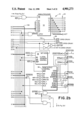
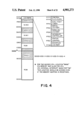
- FIG. 4 is a default memory map showing a preferred arrangement of memory locations in accordance with the invention.
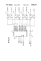
- FIG. 5 is an embodiment of a circuit for providing a plurality of control output signals for NVM access
- FIG. 6 shows a preferred embodiment for providing a signal in response to an illegal address selection
- FIG. 7 shows in schematic form a preferred embodiment of a circuit for providing NVM selection
- FIG. 8 shows in schematic form a status and control circuit arrangement
- FIG. 9 is a schematic of a circuit for control of interrupts to the system microprocessor
- FIG. 10 is a timing diagram of the events.
- FIG. 11 is a timing diagram.
- FIG. 1 is a block diagram of a meter in which the invention may be incorporated.
- Such meters are known and are described forinstance in U.S. Pat. No. 3,978,457 to Check, et al and assigned to the assignee of the present invention, specifically incorporated herein by reference.
- the working memory under control of the CPU is a Random Access Memory from which data must be transferred to anonvolatile memory upon loss or shutdown of power to the meter.
- U.S. Pat. No. 4,481,604 assigned to Roneo Alcatel discloses an electronic postage meter where the Random Access Memory and the nonvolatile storage memories are combined in battery backed CMOS RAMs which are used both for the real time operation and for long term storage of information in postalregisters.
- EPC Application No. 0 085 385 published Aug. 10, 1983, and assigned to the assignee of the present invention discloses an improved dual non-memory system and is specifically incorporated by reference. It will be appreciated by those skilled in the art that such a device may be combined with the electronic postage meter described in Check and is also suitable for the invention disclosed herein.
- decoder arrangement disclosed herein is conveniently used to provide a method and apparatus for further protecting essential postal data in conjunction with the circuit described in application Ser. No. 710,802 filed on even date herewith entitled POSTAGE METER WITH NONVOLATILE MEMORY PROTECTION and assigned to the assignee of the present invention.
- the heart of the general functional arrangement of the system is the CPU which is utilized with specific instructions programmed in the Read Only Memory (PM), for the performance of control ofthe basic meter functions, for the performance of calculations based on anyinput data and for controlling the flow of data into the various memories.
- PM Read Only Memory
- the system may operate in accordance with data applied from an appropriate input means “I” or from a communications means “C” such as described for instance in U.S. Pat. No. 4,301,507 to Soderberg also specifically incorporated herein by reference.
- the data is fed into the CPU under control of the program in Read Only emory and at any time during the operation of the system, should the contents of the memory storing the appropriate credit/debit balances or other cumulations in accordance with various features of the system be desired to be displayed, appropriate instructions provided by the input means "I” cause the CPU to access the desired locations in memory which store the information requested.
- the information may be displayed on an output unit "O".
- the input and output units may be multiplexed by a suitable multiplex unit "MP" for transferring data to and from the CPU.
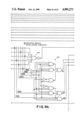
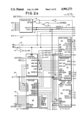
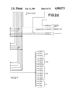
- FIG. 2 is a block diagram of a specific arrangement of a processor interface circuit in accordance with the invention and comprises an address decoder and associated selection circuitry for the selection and control of various elements of the Electronic Postage Meter. It will be appreciated that the circuit arrangement herein described is preferably embodied in a custom LSI microchip, however, it will be understood that the use of conventional logic components is also contemplated.
- the demultiplexer 12 in conventional manner demultiplexesthe address/data bus 14 of a microprocessor (not shown in FIG. 2), suitablyan 8085 series microprocessor available from the Intel Corporation or an NSC800 Series microprocessor available from the National Semiconductor Corporation.
- the bus 14 communicates with the demultiplexer 12 on communication lines 16 through a conventional transceiver circuit arrangement 18.
- ADDRESS LATCH ENABLE (ALE) signal 20 from the microprocessor is "anded" with the microprocessor read strobe signal 22 to provide the latching signal for latching the address information for the demultiplexer 12.
- ALE ADDRESS LATCH ENABLE
- the demultiplexed address information is fed out on lines 24 for use in other parts of the EPM and are internally connected at 26 to the decoder section 28.
- the high order address signals directly from the microprocessor are communicated on lines 30 to the decoder section 26.
- An external decode signal, EXTDEC is also input to the decoder section 28.
- the decoder section 28 receives and decodes a complete input address received at 26 and 30 to provide select outputs for the various parts of the system.
- the low order demultiplexed address lines A0, A1 and A2 are utilized as inputs to control flip-flops 32 along with the microprocessor write strobe WR received at 34 from the microprocessor.
- the control flip-flop section generates four control signals in response to these inputs in addition to a decoder reset signal and other derived signals, i.e. EXT-INTP, a pulse signal generated at the activation of the illegal memory access output pin, and a select signal CONTRL-s for the selection of the Control Flip Flop block.
- NVM output control block 36 Outputs from the decoder 28 are provided to NVM output control block 36.
- This control block 36 in accordance with the invention provides a fail-safe NVM device selection. The selection of either NVM is disabled if the NVM write line is shorted to the "active" state. The NVM write strobe is disabled whenever the other devices are selected or in the event that both NVMs are simultaneously selected.
- an illegal address control block 38 in conjunction with the decoder 28 detects when the microprocessor read or write strobes attempt to access an illegal, i.e. unused, memory space and,as discussed below, provides a signal output for interrupting the processor.
- Status and control block 40 monitors the outputs from the control Flip-Flopsection and provides a control port to generate a decoder reset and to control the selection of an internal or external communication through an "Echoplex" I/0 section 42.
- the section also includes an 8-bit timer to set the Transmit Baud rate for the serial communications.
- Dual Timer section 44 provides two programmable 16-bit timers.
- the system clock is the clock input to the timers.
- each is programmable for continuous or for one-shot operation for generating an interrupt when the programmed count is completed.
- an 8-bit counter divider can be selected to prescale the clock input or the ripple output of the first timer may be selected as the clock input to the secondtimer.
- serial I/O block 46 and parallel I/O block 48 are utilized forcommunication with a keyboard and display and for motor control, sensing postal value and miscellaneous control functions.
- an Interrupt Status and Control Block 50 is provided along with an interrupt mask control port for enabling selected interruptsto interrupt the systems processor.
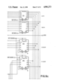
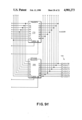
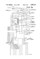
- FIG. 3 shows a schematic of an embodiment of a decoder block for providing a decoded memory map in accordance with the invention.
- the crossed lines with a circle superposed are used to indicate the preferred conductive path in a customized chip arrangement. It will be appreciated that the illustrated arrangement is extremely convenient in that the decoded memorymap as described below may be modified easily with only a few mask changes.
- the various addresses communicated in known manner from the microprocessor and demultiplexer as described previously are each fed to leads A1 throughA15 of the decoder block 28.
- the address bits on address lines A11 through A15 are supplied to NAND gates 52, 54, 56, 58, and 60 and inverted at inverters 62, 64, 66, 68, and 70 and applied as illustrated to the NAND gates 52, 54, 56, and 58.
- An external decode signal 72 (see also FIG. 2) is applied to NAND gate 60.
- the output of NAND gate 60 is NOR'D with the outputs of gates 52, 54, and 56.
- the EXTDEC signal is also applied directed to gate 58. It will be noted that when "active" this signal will disable the decode function.
- the decoded outputs from the connections illustrated in FIG. 3 for the preferred embodiment are as shown in Table Iand in FIG. 4.
- an active DVOID output is provided from NAND gate 74 when one of the system's blocks are selected.
- the address bits when appropriately decoded as in the illustrated circuit by NAND gates 76, 78, 80, 82, 84, and 86 and inverters 88, 90, 92, 94, and 96 provide an "active" output I/O whenever any of the I/O functions is selected and an "active" I/O read output whenever any of the internal circuit functional blocks are selected.
- Address bits A3 and A4 are appliedto 2-to-4 demultiplexer 98 and decoded with other low order address bits for providing output signals as defined in Table I for selecting the appropriate blocks.
- the signal DVOID is not necessarily limited to its previously described function.
- a signal VINT from the control flip-flop block further described below may be used to convert this DVOID signal to another decodeoutput.
- This signal shown as “ECHO/VOID” in FIG. 3 is available if the circuits internal ECHOPLEX block 42 is utilized.
- an external "echoplex” section that is, when thesignal “EXTECHO” is “active” the “ECHO/VOID#” output becomes the “select” signal for the external block and the “select” signal for the internal echoplex section, "ECHO-S" is disabled.
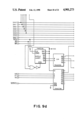
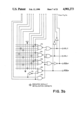
- Control Flip-Flop section 32 As mentioned previously, the Control Flip-Flop section 32, more particularly shown in FIG. 5, generates four control output signals and their complements for controlling the generation of an illegal address interrupt signal to the processor, to provide an independent enable/disable for the access to two separate NVM storage devices, to enable and disable meter postage printing and access to nonvolatile storage.
- the low order address signals A0, A1, and A2 are fedto a 3-to-8 Line Decoder Multiplexer 102 equivalent to a 74HC138 available from RCA to set and reset flip-flops 104, 106, 108, and 110.
- the processorstrobe signal WR and the select signal CNTRL-S are applied to the enable inputs of decoder 102. As illustrated, it is apparent that the control flip-flops are selectively controlled when both these signals are "active".
- the decoder reset signal RST and EXT-INTP (a pulse signal generated at the activation of the illegal memory access interrupt signal) are "NAND'D" at "NAND” gate 112, inverted at inverter and applied to each of the flip-flops 104 and 110.
- Table II shows the preferred decoded control signals in response to the appropriate addresses.
- the outputs from flip-flop 104 designated UNLOCK are preferably active to enable postage printing and for NVM access.
- the preset value is inactive to prevent printing and NVM access.
- the signal WR1-EN and WR2-EN are "active" for write access to respective NVM devices #1 and #2. Again, for best results the preset values are "inactive”.
- the output VINT which as previously discussed is fed to the decoder section28 is active to enable an interrupt generation whenever an illegal memory access is attempted. It will be appreciated that this is preferred since in the "inactive" state it may be used to reset the generated interrupt signal or to disable the interrupt so that it may be used as a spare decode output.
- the VINT preset signal is “active" to enable the interrupt.
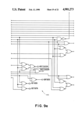
- the illegal address control block 38 is shown more particularly in FIG. 6. This circuit is used to provide an indication of when access to unused memory space is attempted.
- the DVOID decoded signal output from the decoder section 28 is nanded at NAND gate 106 with the Q output from a D Flip-Flop 108.
- the processors read strobe RD and write strobe WR are NAND'D at NAND gate 110, inverted and applied to the clock input of the D flip-flop 108.
- the decoder reset signal is NAND'D with the "VINT" signal from the control flip-flop section32 at NAND gate 112 and applied to the RESET input shown as CLR in the Figure.
- the decoded void memory space indication will be latched at the lead edge of either the read or the write strobe of the microprocessor to provide the output INT-VOID from the Q terminal of flip-flop 108.
- the INT-VOID signal is provided to the system microprocessor as an interrupt signal. Preferably this indication will remain latched until reset by the reset signal from the microprocessor.
- the output is inverted at inverter 116 and supplied at 118 at INT-VOID.
- this INT-VOIDoutput pin in open-drain so as to permit anyof a number of open-drain outputs wire-ored to this pin to activate the output signal.
- This output pin is then suitably tapped as the input signalEXT-INT which is furnished to the Status and Control Block. There, this signal is provided as a status port bit and upon its actuation, a 1 clock period pulse is generated on signal EXT-INTP.
- This EXT-INTP is provided from the status and control section to reset the control flip-flop and parallel I/O sections to their default (safe) states when the INT-VOID output pin is activated.
- the NVM Output Control Block 36 is shown in greaterdetail.
- the WRITE access tothe two independent NVM devices is independently enabled and disabled undersoftware control.
- the NVM OUTPUT CONTROL will block the microprocessor write strobe WR unlesseither of the NVM decoded select signals SEL1 and SEL2 is available and theappropriate write enable signal from the control flip-flops are available at NAND gates 118 and 120.
- the output of these gates are inputs to NAND gate 122 whose output is applied to NAND gate 124.
- the output of this gate is inverted and supplied to NAND gate 126.
- the other signals applied to NAND gate 124 are the decoded select signals NVM1, NVM2, ROM, RAM and VOID are taken from the output drivers and applied to NAND gate 124, with NVM 1 and NVM2 being NOR'D at NOR gate 128 and inverted before being applied to 124. It will be appreciated that the write strobe WR is blocked if the appropriate memory space is not selected. It will also be appreciated that if both NVMs are selected simultaneously the write strobe will also be blocked.
- a further protection feature is provided in the event that the NVM write strobe output is shorted "active".
- the address enable strobe at 20 is applied as the clock signal to a D flip-flop 130. If the NVMWR is shorted active, the ALE signal clocks the Q output low to block both of the NVM device selection signals at NAND gates 132 and 134.
- FIG. 8 is a schematic of the status and control block.
- the block comprises a status port to allow monitoring of the control flip-flop outputs.
- the outputs of the control flip-flop block 32 are applied to buffer 136 for output to data bus 138, see also FIG. 2.
- the system clock input from 140 (see FIG. 2) is used in conventional fashion for timing the internal resetoutput by counting through D flip-flops 142, 144, and 146 to provide signalIRST which is the control signal for resetting all of the flip-flops in thecircuit and is applied along with the System Reset to AND gate 148, (see FIG. 2).
- the block select signal STAT-S for this block, the write strobe, read strobe, and lowest order address bit are decoded to clock the writing of data at octal flip-flop 150, for initiating a general decoder reset under the control of appropriate software commands and for setting a baud-rate divider circuit if desired.
- the EXTECHO signal from D flip-flop 152 is used as previously discussed for selection of an external communication device (not shown).
- the Interrupt Controller block 50 is shown in more detail in FIG. 9.
- the interrupt controller in accordance with the invention provides great flexibility in the servicing of the various interrupt signals to the microprocessor.
- Signal INTA from the system microprocessor is an interrupt acknowledge. It will be appreciated that if the INTA line is held or tied in the "inactive" state, each interrupt signal input applied through gates indicated generally at 156 and fed to NAND gate 158 will create an interrupt request signal INTR for communication to the system's microprocessor.
- mask bits may be fed as data on data input bus16 for providing masking bits to D-flip-flops 160 for latching.
- the latchedoutputs from 160 are applied to gates 156 so that the interrupt request will be generated whenever an unmasked device requests service. The particular device requesting service may be determined by reading the status buffer 154.
- the interrupt lines are also coded at the gates indicated generally at 162 for feeding to latch 164 which also provides similar information.
- a vectored interrupt for the handling of service requests.
- a non-masked interrupt results in the generation of an interrupt-request signal to the systems microprocessor.
- the microprocessor upon receiving this signal will transmit an interrupt acknowledge signal INTA.
- This signal places the contents of the opcode latch 166 onto the data bus.
- the processor interprets this data as an opcode, normally a call instruction for the microprocessor.
- the microprocessor Upon executionof the instruction, the microprocessor generates another INTA pulse to enable the lower vector latch 168.
- the encoding of bits on this latch desirably reflects a predetermined code representing the highest priority interrupt.
- the next INTA pulse in response to the call of this OPCODE, will place the data residing in latch 170, preferably the upper vector address data, onto the data bus 138.
- the INTR-S signal is utilized to select this block.
- the low order address signals A0 through A2 are used as illustrated to decode the various control signals on the gates indicated generally at 140.
- Echoplex circuits suitable for use in block 42 are discussed in U.S. Pat. No. 4,301,507 incorporated by reference herein. Ser. I/O and parallel I/O port circuits are well known and will not be discussed further herein.
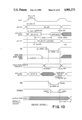
- FIG. 10 and FIG. 11 are timing diagrams showing the interrelationship of signals previously discussed. The designated parameters and preferred timing are shown in TABLE III. It is believed that these diagrams will be readily understood by those skilled in the art so they will not be furtherdescribed except with regard to the operation of the circuit.
- the circuit 10 in accordance with the invention receives and decodes the periodic address signals communicated from the microprocessor and received at decoder block28 and control flip-flop block 32.
- the address signals are decoded to provide an "active" selection signal for each of the various blocks of thecircuit 10 and the memory devices of the electronic postage meter dependingupon the communication of the appropriate addresses for the particular device.
- the DVOID signal from the decoder block 28 goes “active” causing the output of gate 106 (FIG. 6) to go high and latching the Q output of flip-flop 108 active.
- a latched interrupt signal is sent to the interrupt control block 50 for communication to the microprocessor which responds as previously described above in conjunctionwith FIG. 9 whenever an illegal access is attempted.
- Protection is also provided during system power up with the use of the unlock control flip-flop signal. It is a master control of access to the NVM's and postage printing which will disable these functions until the software operating system is ready to enable them.
- the output from gate 126 is not shorted active and so to assure that writing to the NVM is being commandedby the microprocessor, the selection of a nonvolatile memory is blocked if NVMWR is held active.
- the output write enable signal NVMWR is fed to latch130 (FIG. 7) which is clocked by the address-latch-enable signal (ALE) fromthe microprocessor.
- ALE address-latch-enable signal
- NVMWR is active when the ALE signal becomes active, the Q output of latch 130 goes high and blocks the output of gates 132 and 134.
- a nonvolatile memory there must be a periodicallyactive nonvolatile memory write enabling signal and selection of only one nonvolatile memory to assure that the microprocessor is providing the appropriate data to the appropriately selected NVM.
Abstract
An electronic postage meter has an improved memory selection circuit wherein custom memory map decoder circuit with resolution down to a single byte location is used to provide selection enabling signals to insure the selection of an appropriate device only when the addresses appropriate to that device are communicated. In accordance with the invention, at least two nonvolatile memories are provided. Writing to either of these nonvolatile memories is inhibited unless one and only one memory is selected. The circuit also prevents the selection of either of the nonvolatile memories in the event that the write strobe signal to the memories is held active.
Description
The invention relates to postage meters and in particular to electronic postage meters having microcomputer control of printing and accounting functions.
Devices of this type are generally known, and are discussed for example in U.S. Pat. No. 3,978,457. This patent discloses a system for a postage meter which includes a keyboard for the manual introduction of data corresponding to the postage to be printed in a Random Access Memory for real time operation. Data is stored in a nonvolatile memory upon power down and read into the Random Access Memory upon power up.
U.S. Pat. No. 4,481,604 describes an electronic postage meter having a redundant memory system in which for each postal printing operation identical data is stored, respectively, in two separate but identical CMOS battery-backed nonvolatile memories.
In these known devices, there have been found to be times when essential data has not properly been stored in the nonvolatile memory of the meter. It has been found that one reason might be the improper selection of access to a particular device.
In known electronic postage meters, the microprocessor high order address bits or combination thereof are utilized in a standard decoder for selecting or enabling a particular memory or peripheral device to be accessed in accordance with the microcomputer instructions. While this normally works well, in many cases of improper operation of the microcomputer or failure of one of the address lines of the bus, an improper bit may be decoded and the select logic gate which then enables the wrong device may cause wrong data to be read from memory or in the worst case cause data to be written into an unknown memory or peripheral with no indication of any malfunction. When this happens there is a strong possibility of service personnel's not being able to recover essential information from the nonvolatile memory in the postage meter when the postage meter fails.
In accordance with the invention, in order to assure that data is written only to the appropriate nonvolatile memory a logic circuit is provided which will decode the addresses called by the microprocessor in such manner as to ensure the selection of the appropriate memory or device, and particularly the NVM, only when the addresses appropriate to that device are communicated.
It is accordingly a first object of the invention to provide a decoded output which provides the proper select signal only when the appropriate addresses are communicated from the microprocessor so as to particularly insure the reading and writing of the appropriate data into the appropriate location.
It is further object of the invention to provide in an electronic postage meter an address decode logic arrangement with a resolution down to a single byte location.
Other features and objects of the invention will become apparent in conjunction with the description of the drawing wherein;
FIG. 1 is a block diagram of an electronic postage meter in accordance with the invention;
FIGS. 2a-2d are a block diagram of a specific arrangement of a processor interface circuit in accordance with the invention;
FIGS. 3a-3b are a schematic of a decoder arrangement in accordance with the invention;
FIG. 4 is a default memory map showing a preferred arrangement of memory locations in accordance with the invention;
FIG. 5 is an embodiment of a circuit for providing a plurality of control output signals for NVM access;
FIG. 6 shows a preferred embodiment for providing a signal in response to an illegal address selection;
FIG. 7 shows in schematic form a preferred embodiment of a circuit for providing NVM selection;
FIG. 8 shows in schematic form a status and control circuit arrangement;
FIG. 9 is a schematic of a circuit for control of interrupts to the system microprocessor;
FIG. 10 is a timing diagram of the events; and
FIG. 11 is a timing diagram.
Referring now to FIG. 1 which is a block diagram of a meter in which the invention may be incorporated. Such meters are known and are described forinstance in U.S. Pat. No. 3,978,457 to Check, et al and assigned to the assignee of the present invention, specifically incorporated herein by reference. In this referenced patent, the working memory under control of the CPU is a Random Access Memory from which data must be transferred to anonvolatile memory upon loss or shutdown of power to the meter.
U.S. Pat. No. 4,481,604 assigned to Roneo Alcatel discloses an electronic postage meter where the Random Access Memory and the nonvolatile storage memories are combined in battery backed CMOS RAMs which are used both for the real time operation and for long term storage of information in postalregisters. EPC Application No. 0 085 385 published Aug. 10, 1983, and assigned to the assignee of the present invention discloses an improved dual non-memory system and is specifically incorporated by reference. It will be appreciated by those skilled in the art that such a device may be combined with the electronic postage meter described in Check and is also suitable for the invention disclosed herein. The decoder arrangement disclosed herein is conveniently used to provide a method and apparatus for further protecting essential postal data in conjunction with the circuit described in application Ser. No. 710,802 filed on even date herewith entitled POSTAGE METER WITH NONVOLATILE MEMORY PROTECTION and assigned to the assignee of the present invention.
Still referring to FIG. 1, the heart of the general functional arrangement of the system is the CPU which is utilized with specific instructions programmed in the Read Only Memory (PM), for the performance of control ofthe basic meter functions, for the performance of calculations based on anyinput data and for controlling the flow of data into the various memories.
The system may operate in accordance with data applied from an appropriate input means "I" or from a communications means "C" such as described for instance in U.S. Pat. No. 4,301,507 to Soderberg also specifically incorporated herein by reference. The data is fed into the CPU under control of the program in Read Only emory and at any time during the operation of the system, should the contents of the memory storing the appropriate credit/debit balances or other cumulations in accordance with various features of the system be desired to be displayed, appropriate instructions provided by the input means "I" cause the CPU to access the desired locations in memory which store the information requested. The information may be displayed on an output unit "O". As well known, the input and output units may be multiplexed by a suitable multiplex unit "MP" for transferring data to and from the CPU.
FIG. 2 is a block diagram of a specific arrangement of a processor interface circuit in accordance with the invention and comprises an address decoder and associated selection circuitry for the selection and control of various elements of the Electronic Postage Meter. It will be appreciated that the circuit arrangement herein described is preferably embodied in a custom LSI microchip, however, it will be understood that the use of conventional logic components is also contemplated.
Turning now to FIG. 2, the overall block diagram of the circuit is shown generally at 10. The demultiplexer 12 in conventional manner demultiplexesthe address/data bus 14 of a microprocessor (not shown in FIG. 2), suitablyan 8085 series microprocessor available from the Intel Corporation or an NSC800 Series microprocessor available from the National Semiconductor Corporation. The bus 14 communicates with the demultiplexer 12 on communication lines 16 through a conventional transceiver circuit arrangement 18. For best results the ADDRESS LATCH ENABLE (ALE) signal 20 from the microprocessor is "anded" with the microprocessor read strobe signal 22 to provide the latching signal for latching the address information for the demultiplexer 12.
The demultiplexed address information is fed out on lines 24 for use in other parts of the EPM and are internally connected at 26 to the decoder section 28. The high order address signals directly from the microprocessor are communicated on lines 30 to the decoder section 26. An external decode signal, EXTDEC, is also input to the decoder section 28.
The decoder section 28 receives and decodes a complete input address received at 26 and 30 to provide select outputs for the various parts of the system. The low order demultiplexed address lines A0, A1 and A2 are utilized as inputs to control flip-flops 32 along with the microprocessor write strobe WR received at 34 from the microprocessor. As described further below, the control flip-flop section generates four control signals in response to these inputs in addition to a decoder reset signal and other derived signals, i.e. EXT-INTP, a pulse signal generated at the activation of the illegal memory access output pin, and a select signal CONTRL-s for the selection of the Control Flip Flop block.
Outputs from the decoder 28 are provided to NVM output control block 36. This control block 36 in accordance with the invention provides a fail-safe NVM device selection. The selection of either NVM is disabled ifthe NVM write line is shorted to the "active" state. The NVM write strobe is disabled whenever the other devices are selected or in the event that both NVMs are simultaneously selected.
In accordance with the invention, an illegal address control block 38, in conjunction with the decoder 28 detects when the microprocessor read or write strobes attempt to access an illegal, i.e. unused, memory space and,as discussed below, provides a signal output for interrupting the processor.
Status and control block 40 monitors the outputs from the control Flip-Flopsection and provides a control port to generate a decoder reset and to control the selection of an internal or external communication through an "Echoplex" I/0 section 42. Preferably the section also includes an 8-bit timer to set the Transmit Baud rate for the serial communications.
Dual Timer section 44 provides two programmable 16-bit timers. Preferably the system clock is the clock input to the timers. Suitably each is programmable for continuous or for one-shot operation for generating an interrupt when the programmed count is completed. Conveniently an 8-bit counter divider can be selected to prescale the clock input or the ripple output of the first timer may be selected as the clock input to the secondtimer.
Conveniently serial I/O block 46 and parallel I/O block 48 are utilized forcommunication with a keyboard and display and for motor control, sensing postal value and miscellaneous control functions.
For best results, an Interrupt Status and Control Block 50 is provided along with an interrupt mask control port for enabling selected interruptsto interrupt the systems processor.
FIG. 3 shows a schematic of an embodiment of a decoder block for providing a decoded memory map in accordance with the invention. The crossed lines with a circle superposed are used to indicate the preferred conductive path in a customized chip arrangement. It will be appreciated that the illustrated arrangement is extremely convenient in that the decoded memorymap as described below may be modified easily with only a few mask changes.
The various addresses communicated in known manner from the microprocessor and demultiplexer as described previously are each fed to leads A1 throughA15 of the decoder block 28. The address bits on address lines A11 through A15 are supplied to NAND gates 52, 54, 56, 58, and 60 and inverted at inverters 62, 64, 66, 68, and 70 and applied as illustrated to the NAND gates 52, 54, 56, and 58. An external decode signal 72 (see also FIG. 2) is applied to NAND gate 60. The output of NAND gate 60 is NOR'D with the outputs of gates 52, 54, and 56. The EXTDEC signal is also applied directed to gate 58. It will be noted that when "active" this signal will disable the decode function. The decoded outputs from the connections illustrated in FIG. 3 for the preferred embodiment are as shown in Table Iand in FIG. 4.
                                  TABLE I
__________________________________________________________________________
OUTPUTS
__________________________________________________________________________
ROM#      SELECT FOR EXTERNAL PROM MEMORY
RAM#      SELECT FOR EXTERNAL RAM MEMORY
SEL1      FOR GENERATING THE SELECT FOR EXTERNAL NVM#1
SEL2      FOR GENERATING THE SELECT FOR EXTERNAL NVM#2
CNTRL-S   SELECT FOR INTERNAL CONTROL FLIP-FLOP BLOCK
INTR-S    SELECT FOR INTERNAL INTERRUPT CONTROLLER
STAT-S    SELECT FOR INTERNAL STATUS BLOCK
TIMER-S   SELECT FOR INTERNAL DUAL-TIMER BLOCK
ECHO-S    SELECT FOR INTERNAL ECHOPLEX BLOCK
SERIAL-S  SELECT FOR INTERNAL SERIAL I/O BLOCK
PARALLEL-S
          SELECT FOR INTERNAL PARALLEL I/O BLOCK
ECHO/VOID#
          SELECT FOR EXTERNAL ECHOPLEX BLOCK OR SPARE
          DECODE SIGNAL WHEN UNUSED MEMORY SPACE IS
          SELECTED (OR NEITHER)
IO        ACTIVE WHEN ANY I/O SELECTS ARE ACTIVE
IOREAD    ACTIVE WHEN ANY OF THE INTERNAL SELECTS ARE
          ACTIVE
DVOID     ACTIVE WHEN "ExtDec " IS INACTIVE AND WHEN
          NONE OF THE SELECT OUTPUTS ARE ACTIVE
__________________________________________________________________________
OUTPUT SIGNAL ADDRESS RANGE(S)
                           SIZE
__________________________________________________________________________
7FFF          .0..0..0..0. 32   KBYTES
C7FF          C.0..0..0.
              2            KBYTES
D7FF          D.0..0..0.
              2            KBYTES
E7FF          E.0..0..0.
              2            KBYTES
ECHO-S        FFD8 - FFDF  8    BYTES
FFE1-S        FFE.0.
              2            BYTES
INTR-S        FFE2 - FFE7  6    BYTES
PARALLEL-S    FFE8 - FFEB  4    BYTES
SERIAL-S      FFEC - FFEF  4    BYTES
FFF7R-S       FFF.0.
              8            BYTES
CNTRL-S       FFF8 - FFFF  8    BYTES
IO            FFD8 - FFFF  48   BYTES
IOREAD        FFD8 - FFFF; IF "EXTECHO " INACTIVE
FFFF; IF "EXTECHO " ACTIVE
__________________________________________________________________________
It will be noted that in accordance with the invention, an active DVOID output is provided from NAND gate 74 when one of the system's blocks are selected. It will be also be clear to one skilled in the art that the address bits, when appropriately decoded as in the illustrated circuit by NAND gates 76, 78, 80, 82, 84, and 86 and inverters 88, 90, 92, 94, and 96provide an "active" output I/O whenever any of the I/O functions is selected and an "active" I/O read output whenever any of the internal circuit functional blocks are selected. Address bits A3 and A4 are appliedto 2-to-4 demultiplexer 98 and decoded with other low order address bits for providing output signals as defined in Table I for selecting the appropriate blocks.
It will be understood that the signal DVOID is not necessarily limited to its previously described function. For instance, in the illustrated embodiment, a signal VINT from the control flip-flop block further described below may be used to convert this DVOID signal to another decodeoutput. This signal shown as "ECHO/VOID" in FIG. 3 is available if the circuits internal ECHOPLEX block 42 is utilized. Alternatively it will be seen that if an external "echoplex" section is utilized, that is, when thesignal "EXTECHO" is "active" the "ECHO/VOID#" output becomes the "select" signal for the external block and the "select" signal for the internal echoplex section, "ECHO-S" is disabled.
As mentioned previously, the Control Flip-Flop section 32, more particularly shown in FIG. 5, generates four control output signals and their complements for controlling the generation of an illegal address interrupt signal to the processor, to provide an independent enable/disable for the access to two separate NVM storage devices, to enable and disable meter postage printing and access to nonvolatile storage.
As best seen in FIG. 5 the low order address signals A0, A1, and A2 are fedto a 3-to-8 Line Decoder Multiplexer 102 equivalent to a 74HC138 available from RCA to set and reset flip-flops 104, 106, 108, and 110. The processorstrobe signal WR and the select signal CNTRL-S are applied to the enable inputs of decoder 102. As illustrated, it is apparent that the control flip-flops are selectively controlled when both these signals are "active".
The decoder reset signal RST and EXT-INTP (a pulse signal generated at the activation of the illegal memory access interrupt signal) are "NAND'D" at "NAND" gate 112, inverted at inverter and applied to each of the flip-flops 104 and 110. Table II shows the preferred decoded control signals in response to the appropriate addresses.
              TABLE II
______________________________________
     DECODED       FLIP-
A.0.-2
     CNTRL         FLOP      OUTPUT
______________________________________
.0.  VINT-CLR      VINT      INACTIVE
1    VINT-EN       VINT      ACTIVE   PRESET
2    WR2-RESET     WR2-EN    INACTIVE PRESET
3    WR2-SET       WR2-EN    ACTIVE
4    WR1-RESET     WR1-EN    INACTIVE PRESET
5    WR1-SET       WR1-EN    ACTIVE
6    UNLOCK-SET    UNLOCK    ACTIVE
7    UNLOCK-CLR    UNLOCK    INACTIVE PRESET
______________________________________
The outputs from flip-flop 104 designated UNLOCK are preferably active to enable postage printing and for NVM access. For best results, the preset value is inactive to prevent printing and NVM access. The signal WR1-EN and WR2-EN are "active" for write access to respective NVM devices #1 and #2. Again, for best results the preset values are "inactive".
The output VINT which as previously discussed is fed to the decoder section28 is active to enable an interrupt generation whenever an illegal memory access is attempted. It will be appreciated that this is preferred since in the "inactive" state it may be used to reset the generated interrupt signal or to disable the interrupt so that it may be used as a spare decode output. The VINT preset signal is "active" to enable the interrupt.
The illegal address control block 38 is shown more particularly in FIG. 6. This circuit is used to provide an indication of when access to unused memory space is attempted.
The DVOID decoded signal output from the decoder section 28 is nanded at NAND gate 106 with the Q output from a D Flip-Flop 108. The processors read strobe RD and write strobe WR are NAND'D at NAND gate 110, inverted and applied to the clock input of the D flip-flop 108. The decoder reset signal is NAND'D with the "VINT" signal from the control flip-flop section32 at NAND gate 112 and applied to the RESET input shown as CLR in the Figure.
Thus, depending upon the status of the signal VINT as discussed previously,the decoded void memory space indication will be latched at the lead edge of either the read or the write strobe of the microprocessor to provide the output INT-VOID from the Q terminal of flip-flop 108. In accordance with the invention, the INT-VOID signal is provided to the system microprocessor as an interrupt signal. Preferably this indication will remain latched until reset by the reset signal from the microprocessor.
Conveniently as seen in FIG. 2 the output is inverted at inverter 116 and supplied at 118 at INT-VOID.
For best results, this INT-VOIDoutput pin in open-drain so as to permit anyof a number of open-drain outputs wire-ored to this pin to activate the output signal. This output pin is then suitably tapped as the input signalEXT-INT which is furnished to the Status and Control Block. There, this signal is provided as a status port bit and upon its actuation, a 1 clock period pulse is generated on signal EXT-INTP. This EXT-INTP is provided from the status and control section to reset the control flip-flop and parallel I/O sections to their default (safe) states when the INT-VOID output pin is activated.
Turning now the FIG. 7, the NVM Output Control Block 36 is shown in greaterdetail. In order to insure secure accounting in the NVM the WRITE access tothe two independent NVM devices is independently enabled and disabled undersoftware control.
The NVM OUTPUT CONTROL will block the microprocessor write strobe WR unlesseither of the NVM decoded select signals SEL1 and SEL2 is available and theappropriate write enable signal from the control flip-flops are available at NAND gates 118 and 120. The output of these gates are inputs to NAND gate 122 whose output is applied to NAND gate 124. The output of this gateis inverted and supplied to NAND gate 126.
The other signals applied to NAND gate 124 are the decoded select signals NVM1, NVM2, ROM, RAM and VOID are taken from the output drivers and applied to NAND gate 124, with NVM 1 and NVM2 being NOR'D at NOR gate 128 and inverted before being applied to 124. It will be appreciated that the write strobe WR is blocked if the appropriate memory space is not selected. It will also be appreciated that if both NVMs are selected simultaneously the write strobe will also be blocked.
A further protection feature is provided in the event that the NVM write strobe output is shorted "active". The address enable strobe at 20 is applied as the clock signal to a D flip-flop 130. If the NVMWR is shorted active, the ALE signal clocks the Q output low to block both of the NVM device selection signals at NAND gates 132 and 134.
FIG. 8 is a schematic of the status and control block. The block comprises a status port to allow monitoring of the control flip-flop outputs. The outputs of the control flip-flop block 32 are applied to buffer 136 for output to data bus 138, see also FIG. 2. The system clock input from 140 (see FIG. 2) is used in conventional fashion for timing the internal resetoutput by counting through D flip-flops 142, 144, and 146 to provide signalIRST which is the control signal for resetting all of the flip-flops in thecircuit and is applied along with the System Reset to AND gate 148, (see FIG. 2).
The block select signal STAT-S for this block, the write strobe, read strobe, and lowest order address bit are decoded to clock the writing of data at octal flip-flop 150, for initiating a general decoder reset under the control of appropriate software commands and for setting a baud-rate divider circuit if desired. The EXTECHO signal from D flip-flop 152 is used as previously discussed for selection of an external communication device (not shown).
The Interrupt Controller block 50 is shown in more detail in FIG. 9. The interrupt controller in accordance with the invention provides great flexibility in the servicing of the various interrupt signals to the microprocessor. The signal INT-VOID from the illegal address control block38, signals INT-TO and INT-TI generated by the time-out of timers in timer block 44, signal INT-ECHO from the ECHOPLEX block 42 which is "active" to indicate the start of an echoplex message, signal INT-SERIAL from serial I/O block 46 which is "active" when new data is received or when the port is read for sending data, and signal INT-MOTOR from PARALLEL I/O block 48 which is preferably "active" when an illegal motor control output has beencommunicated are each input to the INTERRUPT CONTROLLER block 50. The status of each of these signals may be read out directly from buffer 154 when the RD-INTR signal is "active".
Signal INTA from the system microprocessor is an interrupt acknowledge. It will be appreciated that if the INTA line is held or tied in the "inactive" state, each interrupt signal input applied through gates indicated generally at 156 and fed to NAND gate 158 will create an interrupt request signal INTR for communication to the system's microprocessor. Preferably, mask bits may be fed as data on data input bus16 for providing masking bits to D-flip-flops 160 for latching. The latchedoutputs from 160 are applied to gates 156 so that the interrupt request will be generated whenever an unmasked device requests service. The particular device requesting service may be determined by reading the status buffer 154. The interrupt lines are also coded at the gates indicated generally at 162 for feeding to latch 164 which also provides similar information.
Preferably, as shown, there is also included a vectored interrupt for the handling of service requests. As discussed previously, a non-masked interrupt results in the generation of an interrupt-request signal to the systems microprocessor. For best results, the microprocessor upon receiving this signal will transmit an interrupt acknowledge signal INTA. This signal places the contents of the opcode latch 166 onto the data bus.In accordance with the invention, the processor interprets this data as an opcode, normally a call instruction for the microprocessor. Upon executionof the instruction, the microprocessor generates another INTA pulse to enable the lower vector latch 168. The encoding of bits on this latch as described above. The vector thus generated, desirably reflects a predetermined code representing the highest priority interrupt. The next INTA pulse, in response to the call of this OPCODE, will place the data residing in latch 170, preferably the upper vector address data, onto the data bus 138.
The INTR-S signal is utilized to select this block. The low order address signals A0 through A2 are used as illustrated to decode the various control signals on the gates indicated generally at 140.
Echoplex circuits suitable for use in block 42 are discussed in U.S. Pat. No. 4,301,507 incorporated by reference herein. Ser. I/O and parallel I/O port circuits are well known and will not be discussed further herein.
FIG. 10 and FIG. 11 are timing diagrams showing the interrelationship of signals previously discussed. The designated parameters and preferred timing are shown in TABLE III. It is believed that these diagrams will be readily understood by those skilled in the art so they will not be furtherdescribed except with regard to the operation of the circuit.
                                  TABLE III
__________________________________________________________________________
SYMBOL
      PARAMETER         MIN MAX UNIT
                                    NOTE
__________________________________________________________________________
t.sub.ALE
      ALE STROBE WIDTH  75      ns  CONDITION
t.sub.AHS
      A8-15 SET-UP TIME 5.0.    ns  CONDITION
t.sub.ALS
      ADl-7 SET-UP TIME 4.0.    ns  CONDITION
t.sub.ALH
      ADl-7 HOLD TIME   3.0.    ns  CONDITION
t.sub.ARW
      ALE TO RD  OR WR  STROBE
                        125     ns  CONDITION
t.sub.RDW
      RD  STROBE WIDTH  225     ns  CONDITION
t.sub.WRW
      WR  STROBE WIDTH  22.0.   ns  CONDITION
t.sub.WS
      WRITE DATA SET-UP TIME
                        5.0.
                            ns  CONDITION
t.sub.INW
      INTERRUPT PULSE WIDTH
                        125     ns
t.sub.ACC
      ALE TO VALID DATA     3.0..0.
                                ns
t.sub.ALD
      ALE TO VALID Al-7     5.0.
                                ns  t.sub.ACCMAX - 25.0. ns
t.sub.(CE)PD
      A8-15 TO :
      ROM  ENABLE STROBE    5.0.
                                ns  t.sub.ACCMAX - 25.0. ns
                                    + t.sub.AHMIN
      RAM  ENABLE STROBE    5.0.
                                ns  t.sub.ACCMAX - 25.0. ns
                                    + t.sub.AHMIN
      NVM1  ENABLE STROBE   6.0.
                                ns  t.sub.ACCMAX - 28.0. ns
                                    + t.sub.AHMIN
      NVM2   ENABLE STROBE  6.0.
                                ns  t.sub.ACCMAX - 28.0. ns
                                    + t.sub.AHMIN
      ECHO/VOID  STROBE     7.0.
                                ns  t.sub.ACCMAX - 28.0. ns
                                    + t.sub.AHMIN
t.sub.DS
      INPUT PORT DATA
      SET-UP TIME       5.0.    ns
t.sub.WH
      WRITE DATA HOLD TIME
                        75      ns
t.sub.NWD
      WR  TO NVMWR  DELAY   35  ns  t.sub.WHMIN - t.sub.NWDMAX
t.sub.NVMH
      WRITE DATA HOLD TIME
      AFTER NVMWR           5.0.
                                ns  t.sub.WHMIN - t.sub.NWD
t.sub.DO
      WR  TO OUTPUT PORT
      DATA VALID            75  ns  t.sub.WHMIN
t.sub.RH
      Al-7 HOLD TIME AFTER RD
                        .0.     ns
t.sub.RDH
      DATA HOLD TIME AFTER RD
                        .0. 5.0.
                                ns
t.sub.RWI
      RD  OR WR  TO INTR    9.0.
                                ns
t.sub.DMLT
      DMLDIS  TO Al-7 FLOAT 25  ns
t.sub.EXT
      EXTDEC  to CE's FLOAT 25  ns
__________________________________________________________________________
The operation of the circuit has been particularly described with respect to each of the functional units. Broadly, however, the circuit 10 in accordance with the invention receives and decodes the periodic address signals communicated from the microprocessor and received at decoder block28 and control flip-flop block 32. The address signals are decoded to provide an "active" selection signal for each of the various blocks of thecircuit 10 and the memory devices of the electronic postage meter dependingupon the communication of the appropriate addresses for the particular device. In the event that an illegal address is communicated either because of a microprocessor or software failure or because of a failure inthe instant circuit, the DVOID signal from the decoder block 28 goes "active" causing the output of gate 106 (FIG. 6) to go high and latching the Q output of flip-flop 108 active. Thus a latched interrupt signal is sent to the interrupt control block 50 for communication to the microprocessor which responds as previously described above in conjunctionwith FIG. 9 whenever an illegal access is attempted.
As discussed previously, further protection is provided in the event that both nonvolatile memories are selected. As seen in FIG. 7, if both the NVM1 and the NVM2 signals are active the output of gate 128 is high. This output is inverted and applied to gate 124 whose output is then held high so long as both devices are selected. The output of 124 is inverted and the low input to gate 126 blocks the microprocessor's write strobe WR to the NVM. It will also be appreciated that an additional interlock exists on the write access to each NVM by way of control flip-flops WR1-EN and WR2-EN. Under software control, write access is provided to NVM1 only whenWR1-EN is set. Similarly, write access is provided to NVM2 only when WR2-ENis set.
Protection is also provided during system power up with the use of the unlock control flip-flop signal. It is a master control of access to the NVM's and postage printing which will disable these functions until the software operating system is ready to enable them.
In order to assure that signal NVMWR, the output from gate 126 is not shorted active and so to assure that writing to the NVM is being commandedby the microprocessor, the selection of a nonvolatile memory is blocked if NVMWR is held active. The output write enable signal NVMWR is fed to latch130 (FIG. 7) which is clocked by the address-latch-enable signal (ALE) fromthe microprocessor. The Q output from the latch which is normally high is used to enable gates 132 and 134.
If NVMWR is active when the ALE signal becomes active, the Q output of latch 130 goes high and blocks the output of gates 132 and 134. Thus in order for a nonvolatile memory to be selected there must be a periodicallyactive nonvolatile memory write enabling signal and selection of only one nonvolatile memory to assure that the microprocessor is providing the appropriate data to the appropriately selected NVM.
It will be understood that the claims are intended to cover all changes andmodifications of the embodiment herein chosen for the purpose of illustration which do not constitute departures from the scope and spirit of the invention.
Claims (3)
1. In a postage meter having a microprocessor for controlling the printing of value and for accounting for the printing of such value, a first non-volatile memory for storage of accounting data, said microprocessor controlling the printing and accounting in accordance with a program stored in another memory, the first non-volatile memory having a first range of predetermined addresses for accessing thereof by said microprocessor, the improvement comprising selection means connected to the microprocessor to receive address information and to compare it to the first range for providing a first signal whenever the microprocessor selects addresses within said first range, the microprocessor also providing address information at a predetermined address that does not include addresses of said first range, decoding means responsive to said address information at a predetermined address for producing a second signal of longer duration than said address information at a predetermined address, and means responsive to said first and second signals for producing an enabling signal to enable access to said non-volatile memory so as to assure that the selection of the non-volatile memory by the microprocessor is not due to erroneous address information.
2. The device of claim 1 further comprising a second non-volatile memory coupled to receive data and address information from said microprocessor and connected to said selection means, said second non-volatile memory having a second range of predetermined addresses associated therewith for access thereto, said selection means receiving address signals from the microprocessor for producing said first signal in accordance with the address information received from said microprocessor in said second range.
3. A postage meter comprising a microprocessor, a printing means for printing postal value under control of the microprocessor, a plurality of memory means connected to said microprocessor for communication of information therebetween, said memory means including a ROM for storing a program for operation of the microprocessor and a non-volatile memory for storing accounting data for accounting for postal value printed by said printing means, each of said plurality of said memory means having distinct predetermined addresses associated respectively therewith, and further comprising selection means coupled to said microprocessor and said plurality of memory means, said selection means receiving address signals from the microprocessor to produce a first signal when said address signals are in accordance with the predetermined addresses of said non-volatile memory, said microprocessor comprising means for providing an address signal of a predetermined address that is not within said predetermined addresses, and further comprising means for decoding said address signal to provide a second signal of longer duration than said address signal, and means responsive to said first and second signals to enable access to said non-volatile memory so as to assure that access to the non-volatile memory is not due to erroneous address information.
Priority Applications (4)
| Application Number | Priority Date | Filing Date | Title |
|---|---|---|---|
| US06/710,800 US4901273A (en) | 1985-03-12 | 1985-03-12 | Electronic postage meter having a memory map decoder |
| CA000503777A CA1250052A (en) | 1985-03-12 | 1986-03-11 | Electronic postage meter having a memory map decoder |
| EP86103281A EP0194660B1 (en) | 1985-03-12 | 1986-03-12 | Electronic postage meter having a memory map decoder and an illegal-memory-access warning signal, respectively |
| DE8686103281T DE3684496D1 (en) | 1985-03-12 | 1986-03-12 | Franking machine with a decoder of the memory routinelist, or WITH A WARNING SIGNAL ABOUT ILLEGAL MEMORY ACCESS. |
Applications Claiming Priority (1)
| Application Number | Priority Date | Filing Date | Title |
|---|---|---|---|
| US06/710,800 US4901273A (en) | 1985-03-12 | 1985-03-12 | Electronic postage meter having a memory map decoder |
Publications (1)
| Publication Number | Publication Date |
|---|---|
| US4901273A true US4901273A (en) | 1990-02-13 |
Family
ID=24855600
Family Applications (1)
| Application Number | Title | Priority Date | Filing Date |
|---|---|---|---|
| US06/710,800 Expired - Lifetime US4901273A (en) | 1985-03-12 | 1985-03-12 | Electronic postage meter having a memory map decoder |
Country Status (2)
| Country | Link |
|---|---|
| US (1) | US4901273A (en) |
| CA (1) | CA1250052A (en) |
Cited By (2)
| Publication number | Priority date | Publication date | Assignee | Title |
|---|---|---|---|---|
| US5546561A (en) * | 1991-02-11 | 1996-08-13 | Intel Corporation | Circuitry and method for selectively protecting the integrity of data stored within a range of addresses within a non-volatile semiconductor memory |
| US20020131085A1 (en) * | 2001-03-15 | 2002-09-19 | Kazunori Kobayashi | Nonvolatile memory life prolonging circuit and image forming apparatus |
Citations (10)
| Publication number | Priority date | Publication date | Assignee | Title |
|---|---|---|---|---|
| US3938095A (en) * | 1971-11-04 | 1976-02-10 | Pitney-Bowes, Inc. | Computer responsive postage meter |
| US3978457A (en) * | 1974-12-23 | 1976-08-31 | Pitney-Bowes, Inc. | Microcomputerized electronic postage meter system |
| US4038645A (en) * | 1976-04-30 | 1977-07-26 | International Business Machines Corporation | Non-translatable storage protection control system |
| US4053735A (en) * | 1975-08-07 | 1977-10-11 | Foudos James N | Assured-check computer-based bank credit disbursing system |
| US4087856A (en) * | 1976-06-30 | 1978-05-02 | International Business Machines Corporation | Location dependence for assuring the security of system-control operations |
| GB2101370A (en) * | 1981-06-26 | 1983-01-12 | Philips Electronic Associated | Digital data apparatus with memory interrogation |
| US4506364A (en) * | 1982-09-30 | 1985-03-19 | International Business Machines Corporation | Memory address permutation apparatus |
| US4566106A (en) * | 1982-01-29 | 1986-01-21 | Pitney Bowes Inc. | Electronic postage meter having redundant memory |
| US4573119A (en) * | 1983-07-11 | 1986-02-25 | Westheimer Thomas O | Computer software protection system |
| US4584666A (en) * | 1984-06-21 | 1986-04-22 | Motorola, Inc. | Method and apparatus for signed and unsigned bounds check |
-
1985
- 1985-03-12 US US06/710,800 patent/US4901273A/en not_active Expired - Lifetime
-
1986
- 1986-03-11 CA CA000503777A patent/CA1250052A/en not_active Expired
Patent Citations (10)
| Publication number | Priority date | Publication date | Assignee | Title |
|---|---|---|---|---|
| US3938095A (en) * | 1971-11-04 | 1976-02-10 | Pitney-Bowes, Inc. | Computer responsive postage meter |
| US3978457A (en) * | 1974-12-23 | 1976-08-31 | Pitney-Bowes, Inc. | Microcomputerized electronic postage meter system |
| US4053735A (en) * | 1975-08-07 | 1977-10-11 | Foudos James N | Assured-check computer-based bank credit disbursing system |
| US4038645A (en) * | 1976-04-30 | 1977-07-26 | International Business Machines Corporation | Non-translatable storage protection control system |
| US4087856A (en) * | 1976-06-30 | 1978-05-02 | International Business Machines Corporation | Location dependence for assuring the security of system-control operations |
| GB2101370A (en) * | 1981-06-26 | 1983-01-12 | Philips Electronic Associated | Digital data apparatus with memory interrogation |
| US4566106A (en) * | 1982-01-29 | 1986-01-21 | Pitney Bowes Inc. | Electronic postage meter having redundant memory |
| US4506364A (en) * | 1982-09-30 | 1985-03-19 | International Business Machines Corporation | Memory address permutation apparatus |
| US4573119A (en) * | 1983-07-11 | 1986-02-25 | Westheimer Thomas O | Computer software protection system |
| US4584666A (en) * | 1984-06-21 | 1986-04-22 | Motorola, Inc. | Method and apparatus for signed and unsigned bounds check |
Cited By (3)
| Publication number | Priority date | Publication date | Assignee | Title |
|---|---|---|---|---|
| US5546561A (en) * | 1991-02-11 | 1996-08-13 | Intel Corporation | Circuitry and method for selectively protecting the integrity of data stored within a range of addresses within a non-volatile semiconductor memory |
| US20020131085A1 (en) * | 2001-03-15 | 2002-09-19 | Kazunori Kobayashi | Nonvolatile memory life prolonging circuit and image forming apparatus |
| US7221468B2 (en) * | 2001-03-15 | 2007-05-22 | Ricoh Company, Ltd. | Nonvolatile memory life prolonging circuit and image forming apparatus |
Also Published As
| Publication number | Publication date |
|---|---|
| CA1250052A (en) | 1989-02-14 |
Similar Documents
| Publication | Publication Date | Title |
|---|---|---|
| US4710882A (en) | Electronic postage meter having a nonvolatile memory selection means | |
| US4694394A (en) | Microprocessor system having a multiplexed address/data bus which communicates with a plurality of memory and input/output devices including TTL output gates | |
| US3938095A (en) | Computer responsive postage meter | |
| US4566106A (en) | Electronic postage meter having redundant memory | |
| GB2080205A (en) | A postage meter | |
| US4998203A (en) | Postage meter with a non-volatile memory security circuit | |
| US5954813A (en) | Data processor with transparent operation during a background mode and method therefor | |
| US4525785A (en) | Electronic postage meter having plural computing system | |
| US4747057A (en) | Electronic postage meter having power up and power down protection circuitry | |
| US4901273A (en) | Electronic postage meter having a memory map decoder | |
| EP0194660B1 (en) | Electronic postage meter having a memory map decoder and an illegal-memory-access warning signal, respectively | |
| US4916623A (en) | Electronic postage meter having redundant memory | |
| US4706215A (en) | Data protection system for electronic postage meters having multiple non-volatile multiple memories | |
| JPS59112380A (en) | Method and apparatus for controlling farm ware branch point for electronic postage meter | |
| US4701856A (en) | Reset delay circuit for an electronic postage meter | |
| US4635223A (en) | Fail safe protection circuitry for a commerical microprocessor in encryption equipment | |
| US5552991A (en) | Control system for an electronic pastage meter having a programmable application specific intergrated circuit | |
| US5438519A (en) | Electronic postage meter having memory write access second chance hard timer means | |
| GB1577592A (en) | Data processing apparatus | |
| US4635204A (en) | Postal meter with date check reminder means | |
| US4611282A (en) | Postage meter using a flag to indicate interuption of accounting register updating due to power failure or microprocessor failure | |
| EP0356052B1 (en) | Franking machine | |
| US4509141A (en) | Postage meter with keyboard keys used for changing operating constants | |
| US5109507A (en) | Electronic postage meter having redundant memory | |
| US5974402A (en) | Address decoder with memory wait state circuit |
Legal Events
| Date | Code | Title | Description |
|---|---|---|---|
| AS | Assignment |
Owner name: PITNEY BOWES INC., WALTER H. WHEELER, JR. DRIVE ST Free format text: ASSIGNMENT OF ASSIGNORS INTEREST.;ASSIGNOR:DI GIULIO, PETER C.;REEL/FRAME:004382/0540 Effective date: 19850211 |
|
| STCF | Information on status: patent grant |
Free format text: PATENTED CASE |
|
| FEPP | Fee payment procedure |
Free format text: PAYOR NUMBER ASSIGNED (ORIGINAL EVENT CODE: ASPN); ENTITY STATUS OF PATENT OWNER: LARGE ENTITY |
|
| FPAY | Fee payment |
Year of fee payment: 4 |
|
| FPAY | Fee payment |
Year of fee payment: 8 |
|
| FPAY | Fee payment |
Year of fee payment: 12 |