US4675813A - Program assignable I/O addresses for a computer - Google Patents
Program assignable I/O addresses for a computer Download PDFInfo
- Publication number
- US4675813A US4675813A US06/688,548 US68854885A US4675813A US 4675813 A US4675813 A US 4675813A US 68854885 A US68854885 A US 68854885A US 4675813 A US4675813 A US 4675813A
- Authority
- US
- United States
- Prior art keywords
- address
- input
- memory
- unit
- output
- Prior art date
- Legal status (The legal status is an assumption and is not a legal conclusion. Google has not performed a legal analysis and makes no representation as to the accuracy of the status listed.)
- Expired - Lifetime
Links
Images
Classifications
-
- G—PHYSICS
- G06—COMPUTING; CALCULATING OR COUNTING
- G06F—ELECTRIC DIGITAL DATA PROCESSING
- G06F12/00—Accessing, addressing or allocating within memory systems or architectures
-
- G—PHYSICS
- G06—COMPUTING; CALCULATING OR COUNTING
- G06F—ELECTRIC DIGITAL DATA PROCESSING
- G06F12/00—Accessing, addressing or allocating within memory systems or architectures
- G06F12/02—Addressing or allocation; Relocation
- G06F12/06—Addressing a physical block of locations, e.g. base addressing, module addressing, memory dedication
- G06F12/0646—Configuration or reconfiguration
- G06F12/0653—Configuration or reconfiguration with centralised address assignment
- G06F12/0661—Configuration or reconfiguration with centralised address assignment and decentralised selection
Definitions
- This invention relates to an arrangement for addressing a peripheral input/output (I/O) unit for a computer and more particularly to one in which the I/O addresses are program assignable.
- I/O peripheral input/output
- IBM PC International Business Machines' personal computer
- 1024 I/O addresses ranging from hexadecimal 000 to 3FF, with 8 to 16 of these addresses being typically assigned to each peripheral unit. While 1024 I/O addresses are adequate to support any anticipated combination of I/O units which might be installed in a particular IBM PC, they are not adequate to allow each unit type being marketed to have one or more addresses assigned for its exclusive use. As a result, one or more I/O units installed in the same computer (particularly those from different manufacturers) could have overlapping I/O addresses.
- switches in the I/O units so that the addresses are hardware programmable.
- the switches are then programmed so as to avoid any conflict between addresses of the peripheral units installed in a particular computer.
- the hardware switches when programmed, the software in the computer must also be changed so that it will access the new hardware programmed addresses. It will be evident that such an arrangement is both costly to manufacture and time consuming to install because the computer must be disassembled. This disassembly and reassembly process could result in damage to the I/O unit or the computer whenever the switch positions are being altered.
- the present invention provides a unique solution to this problem by providing circuitry in the I/O unit for receiving data that defines the programmable I/O address or group of I/O addresses. This data however is written to a memory address which corresponds to one in the read only memory (ROM) of the main memory of the computer.
- ROM read only memory
- an input/output unit for a computer in which the computer comprises a random access memory (RAM) which responds to a first set of memory addresses, a read only memory (ROM) which responds to a non-overlapping second set of memory addresses, and a microprocessor for selectively addressing the read only memory to read data therefrom when applying a memory read control signal thereto, and for selectively addressing the random access memory to read data therefrom or write data thereto when applying respectively memory read or write control signals thereto.
- the I/O unit is characterized by a register for receiving data from the microprocessor in the presence of a memory write control signal and a particular address which is a duplicate of one in the ROM area of memory.
- the first is an initiating address which is used to establish contact between the peripheral I/O unit and the computer after a power-up or reset.
- the second is a programmable I/O operating address which provides the communication link to the computer once established.
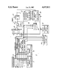
- the peripheral I/O unit 10 of the invention is shown connected to a general purpose microcomputer 11, which for illustrative purposes has the same address or memory map as the IBM PC.
- a conventional known type of peripheral I/O unit 30 is also shown to illustrate the difference in structure between it and the unit 10.
- the computer 11 includes a microprocessor 12 which is coupled via a 20-bit address bus 13, an 8-bit data bus 14, a memory write strobe 15 and a memory read strobe 16 to a random access memory (RAM) 17 which has been assigned a first set of hexadecimal addresses 00000 to 3FFFF (basic system) or to 9FFFF (extended system).
- the address and data buses 13 and 14 and the read strobe 16 from the microprocessor 12 are also connected to a read only memory (ROM) which has been assigned a second non-overlapping set of hexadecimal addresses F0000 to FFFFF.
- ROM read only memory
- the peripheral unit 10 comprises an AND gate 20 having inverted and non-inverted inputs connected to the address bus 13 so as to respond to an initiating address hexadecimal FFF8E which is within the range of the second set of addresses assigned to the ROM 18.
- the microprocessor 12 concurrently transmits this address on the bus 13, and a memory write strobe on the lead 15.
- the simultaneous presence of these two signals produces an output from AND gate 21 which in turn sets a D-type flip-flop 22 and strobes an I/O address register 23 to store data being transmitted simultaneously on the bus 14.
- this data is the 8 of 10 most significant bits of the I/O operating address which ranges from hexadecimal 000 to 3FF.
- the AND gate 21 is disabled by the Q output of the D-type flip-flop 22 which is connected to the gate's inverted input via a switch 24.
- the register 23 is then latched with this address.
- This Q output also enables an I/O match detector 25 which has one input connected to the output of the I/O address register 23 and the other input to the address bus 13.
- the peripheral unit 10 does not respond to any I/O address until after data defining the 8 most significant bits of the 10-bit I/O address has been transmitted via the data bus 14 to the register 23. Thereafter, any transmission of this I/O address on the bus 13 will result in a match being detected in the address match detector 25 which generates a gating signal that in conjunction with control signals on either I/O read or write strobes 27 or 28, transfers data to or from an I/O unit 26 on the data bus 14.
- the conventional peripheral I/O unit 30 includes a preset I/O address match detector 32 which enables an I/O unit 33 whenever there is a match between it and the incoming 10-bit I/O address on the bus 13.
- the I/O unit 33 then transmits or receives data on the bus 14 under control of the I/O read or write strobes 27 or 28 in a well known manner.
- no alteration in this operating I/O address is possible since it is preset by the hardware in the unit 30.
- data can be written to the peripheral unit 10 at several different ROM addresses so that a complete 20-bit operating address can be transmitted over the 8-bit data bus 14.
- consecutive data can be written to the same ROM address in the peripheral unit 10. It will be evident however that no information can be read from the peripheral unit 10 at these ROM addresses since any attempt to do so would clash with information stored in the corresponding address of the ROM 18.
Abstract
Description
Claims (6)
Priority Applications (6)
| Application Number | Priority Date | Filing Date | Title |
|---|---|---|---|
| US06/688,548 US4675813A (en) | 1985-01-03 | 1985-01-03 | Program assignable I/O addresses for a computer |
| CA000476374A CA1217873A (en) | 1985-01-03 | 1985-03-13 | Program assignable i/o addresses for a computer |
| DE8585308349T DE3573849D1 (en) | 1985-01-03 | 1985-11-15 | Program assignable i/o addresses for a computer |
| EP85308349A EP0187453B1 (en) | 1985-01-03 | 1985-11-15 | Program assignable i/o addresses for a computer |
| KR1019850009426A KR870006466A (en) | 1985-01-03 | 1985-12-16 | Programmable Input / Output Address Providing Circuit for Computer |
| JP60293341A JPS61163457A (en) | 1985-01-03 | 1985-12-27 | Peripheral input/output unit |
Applications Claiming Priority (1)
| Application Number | Priority Date | Filing Date | Title |
|---|---|---|---|
| US06/688,548 US4675813A (en) | 1985-01-03 | 1985-01-03 | Program assignable I/O addresses for a computer |
Publications (1)
| Publication Number | Publication Date |
|---|---|
| US4675813A true US4675813A (en) | 1987-06-23 |
Family
ID=24764853
Family Applications (1)
| Application Number | Title | Priority Date | Filing Date |
|---|---|---|---|
| US06/688,548 Expired - Lifetime US4675813A (en) | 1985-01-03 | 1985-01-03 | Program assignable I/O addresses for a computer |
Country Status (6)
| Country | Link |
|---|---|
| US (1) | US4675813A (en) |
| EP (1) | EP0187453B1 (en) |
| JP (1) | JPS61163457A (en) |
| KR (1) | KR870006466A (en) |
| CA (1) | CA1217873A (en) |
| DE (1) | DE3573849D1 (en) |
Cited By (20)
| Publication number | Priority date | Publication date | Assignee | Title |
|---|---|---|---|---|
| US4875158A (en) * | 1985-08-14 | 1989-10-17 | Apple Computer, Inc. | Method for requesting service by a device which generates a service request signal successively until it is serviced |
| US4910655A (en) * | 1985-08-14 | 1990-03-20 | Apple Computer, Inc. | Apparatus for transferring signals and data under the control of a host computer |
| US4912627A (en) * | 1985-08-14 | 1990-03-27 | Apple Computer, Inc. | Method for storing a second number as a command address of a first peripheral device and a third number as a command address of a second peripheral device |
| US4918598A (en) * | 1985-08-14 | 1990-04-17 | Apple Computer, Inc. | Method for selectively activating and deactivating devices having same first address and different extended addresses |
| US5093776A (en) * | 1989-06-15 | 1992-03-03 | Wang Laboratories, Inc. | Information processing system emulation apparatus and method |
| US5274771A (en) * | 1991-04-30 | 1993-12-28 | Hewlett-Packard Company | System for configuring an input/output board in a computer |
| US5367640A (en) * | 1991-04-30 | 1994-11-22 | Hewlett-Packard Company | System for configuring an input/output board in a computer |
| US5491830A (en) * | 1992-05-11 | 1996-02-13 | Westinghouse Air Brake Company | Automatic slot identification and address decoder arrangement |
| US5522086A (en) * | 1993-10-29 | 1996-05-28 | Sierra Semiconductor Canada, Inc. | Software configurable ISA bus card interface with security access read and write sequence to upper data bits at addresses used by a game device |
| US5561813A (en) * | 1993-08-27 | 1996-10-01 | Advanced System Products, Inc. | Circuit for resolving I/O port address conflicts |
| US5590374A (en) * | 1993-09-10 | 1996-12-31 | Fujitsu Limited | Method and apparatus for employing a dummy read command to automatically assign a unique memory address to an interface card |
| US5634075A (en) * | 1995-01-11 | 1997-05-27 | Cirrus Logic, Inc. | Backward compatibility for plug and play systems |
| US5638334A (en) * | 1990-04-18 | 1997-06-10 | Rambus Inc. | Integrated circuit I/O using a high performance bus interface |
| US5664221A (en) * | 1995-11-14 | 1997-09-02 | Digital Equipment Corporation | System for reconfiguring addresses of SCSI devices via a device address bus independent of the SCSI bus |
| US5991841A (en) * | 1997-09-24 | 1999-11-23 | Intel Corporation | Memory transactions on a low pin count bus |
| US6119189A (en) * | 1997-09-24 | 2000-09-12 | Intel Corporation | Bus master transactions on a low pin count bus |
| US6131127A (en) * | 1997-09-24 | 2000-10-10 | Intel Corporation | I/O transactions on a low pin count bus |
| US6157970A (en) * | 1997-09-24 | 2000-12-05 | Intel Corporation | Direct memory access system using time-multiplexing for transferring address, data, and control and a separate control line for serially transmitting encoded DMA channel number |
| US20020129303A1 (en) * | 1999-08-16 | 2002-09-12 | Marko Karppanen | Method and device for improving the reliability of a computer system |
| US11249904B2 (en) * | 2017-11-17 | 2022-02-15 | Mitsubishi Heavy Industries Machinery Systems, Ltd. | Information processing system and information processing method to be executed by information processing system |
Families Citing this family (2)
| Publication number | Priority date | Publication date | Assignee | Title |
|---|---|---|---|---|
| JP2644554B2 (en) * | 1988-11-15 | 1997-08-25 | 株式会社日立製作所 | Information processing system |
| US5781796A (en) * | 1995-06-06 | 1998-07-14 | Lg Semicon Co., Ltd. | System for automatic configuration of I/O base address without configuration program using readout data on common bus by responding device |
Citations (3)
| Publication number | Priority date | Publication date | Assignee | Title |
|---|---|---|---|---|
| US4025903A (en) * | 1973-09-10 | 1977-05-24 | Computer Automation, Inc. | Automatic modular memory address allocation system |
| US4026555A (en) * | 1975-03-12 | 1977-05-31 | Alpex Computer Corporation | Television display control apparatus |
| US4307447A (en) * | 1979-06-19 | 1981-12-22 | Gould Inc. | Programmable controller |
Family Cites Families (3)
| Publication number | Priority date | Publication date | Assignee | Title |
|---|---|---|---|---|
| AT355354B (en) * | 1978-08-29 | 1980-02-25 | Schrack Elektrizitaets Ag E | CIRCUIT ARRANGEMENT WITH A CENTRAL UNIT TO WHICH SEVERAL PERIPHERAL DEVICES ARE CONNECTED |
| US4373181A (en) * | 1980-07-30 | 1983-02-08 | Chisholm Douglas R | Dynamic device address assignment mechanism for a data processing system |
| US4475176A (en) * | 1981-08-06 | 1984-10-02 | Tokyo Shibaura Denki Kabushiki Kaisha | Memory control system |
-
1985
- 1985-01-03 US US06/688,548 patent/US4675813A/en not_active Expired - Lifetime
- 1985-03-13 CA CA000476374A patent/CA1217873A/en not_active Expired
- 1985-11-15 EP EP85308349A patent/EP0187453B1/en not_active Expired
- 1985-11-15 DE DE8585308349T patent/DE3573849D1/en not_active Expired
- 1985-12-16 KR KR1019850009426A patent/KR870006466A/en not_active Application Discontinuation
- 1985-12-27 JP JP60293341A patent/JPS61163457A/en active Pending
Patent Citations (3)
| Publication number | Priority date | Publication date | Assignee | Title |
|---|---|---|---|---|
| US4025903A (en) * | 1973-09-10 | 1977-05-24 | Computer Automation, Inc. | Automatic modular memory address allocation system |
| US4026555A (en) * | 1975-03-12 | 1977-05-31 | Alpex Computer Corporation | Television display control apparatus |
| US4307447A (en) * | 1979-06-19 | 1981-12-22 | Gould Inc. | Programmable controller |
Cited By (29)
| Publication number | Priority date | Publication date | Assignee | Title |
|---|---|---|---|---|
| US4875158A (en) * | 1985-08-14 | 1989-10-17 | Apple Computer, Inc. | Method for requesting service by a device which generates a service request signal successively until it is serviced |
| US4910655A (en) * | 1985-08-14 | 1990-03-20 | Apple Computer, Inc. | Apparatus for transferring signals and data under the control of a host computer |
| US4912627A (en) * | 1985-08-14 | 1990-03-27 | Apple Computer, Inc. | Method for storing a second number as a command address of a first peripheral device and a third number as a command address of a second peripheral device |
| US4918598A (en) * | 1985-08-14 | 1990-04-17 | Apple Computer, Inc. | Method for selectively activating and deactivating devices having same first address and different extended addresses |
| US5093776A (en) * | 1989-06-15 | 1992-03-03 | Wang Laboratories, Inc. | Information processing system emulation apparatus and method |
| US6085284A (en) * | 1990-04-18 | 2000-07-04 | Rambus Inc. | Method of operating a memory device having a variable data output length and an identification register |
| US6070222A (en) * | 1990-04-18 | 2000-05-30 | Rambus Inc. | Synchronous memory device having identification register |
| US5983320A (en) * | 1990-04-18 | 1999-11-09 | Rambus, Inc. | Method and apparatus for externally configuring and modifying the transaction request response characteristics of a semiconductor device coupled to a bus |
| US5954804A (en) * | 1990-04-18 | 1999-09-21 | Rambus Inc. | Synchronous memory device having an internal register |
| US5928343A (en) * | 1990-04-18 | 1999-07-27 | Rambus Inc. | Memory module having memory devices containing internal device ID registers and method of initializing same |
| US5915105A (en) * | 1990-04-18 | 1999-06-22 | Rambus Inc. | Integrated circuit I/O using a high performance bus interface |
| US5841580A (en) * | 1990-04-18 | 1998-11-24 | Rambus, Inc. | Integrated circuit I/O using a high performance bus interface |
| US5809263A (en) * | 1990-04-18 | 1998-09-15 | Rambus Inc. | Integrated circuit I/O using a high performance bus interface |
| US5638334A (en) * | 1990-04-18 | 1997-06-10 | Rambus Inc. | Integrated circuit I/O using a high performance bus interface |
| US5274771A (en) * | 1991-04-30 | 1993-12-28 | Hewlett-Packard Company | System for configuring an input/output board in a computer |
| US5524269A (en) * | 1991-04-30 | 1996-06-04 | Hewlett-Packard Company | System for activating and configuring an input/output board in a computer |
| US5367640A (en) * | 1991-04-30 | 1994-11-22 | Hewlett-Packard Company | System for configuring an input/output board in a computer |
| US5491830A (en) * | 1992-05-11 | 1996-02-13 | Westinghouse Air Brake Company | Automatic slot identification and address decoder arrangement |
| US5561813A (en) * | 1993-08-27 | 1996-10-01 | Advanced System Products, Inc. | Circuit for resolving I/O port address conflicts |
| US5590374A (en) * | 1993-09-10 | 1996-12-31 | Fujitsu Limited | Method and apparatus for employing a dummy read command to automatically assign a unique memory address to an interface card |
| US5522086A (en) * | 1993-10-29 | 1996-05-28 | Sierra Semiconductor Canada, Inc. | Software configurable ISA bus card interface with security access read and write sequence to upper data bits at addresses used by a game device |
| US5634075A (en) * | 1995-01-11 | 1997-05-27 | Cirrus Logic, Inc. | Backward compatibility for plug and play systems |
| US5664221A (en) * | 1995-11-14 | 1997-09-02 | Digital Equipment Corporation | System for reconfiguring addresses of SCSI devices via a device address bus independent of the SCSI bus |
| US5991841A (en) * | 1997-09-24 | 1999-11-23 | Intel Corporation | Memory transactions on a low pin count bus |
| US6119189A (en) * | 1997-09-24 | 2000-09-12 | Intel Corporation | Bus master transactions on a low pin count bus |
| US6131127A (en) * | 1997-09-24 | 2000-10-10 | Intel Corporation | I/O transactions on a low pin count bus |
| US6157970A (en) * | 1997-09-24 | 2000-12-05 | Intel Corporation | Direct memory access system using time-multiplexing for transferring address, data, and control and a separate control line for serially transmitting encoded DMA channel number |
| US20020129303A1 (en) * | 1999-08-16 | 2002-09-12 | Marko Karppanen | Method and device for improving the reliability of a computer system |
| US11249904B2 (en) * | 2017-11-17 | 2022-02-15 | Mitsubishi Heavy Industries Machinery Systems, Ltd. | Information processing system and information processing method to be executed by information processing system |
Also Published As
| Publication number | Publication date |
|---|---|
| EP0187453A2 (en) | 1986-07-16 |
| CA1217873A (en) | 1987-02-10 |
| DE3573849D1 (en) | 1989-11-23 |
| JPS61163457A (en) | 1986-07-24 |
| EP0187453B1 (en) | 1989-10-18 |
| EP0187453A3 (en) | 1987-09-30 |
| KR870006466A (en) | 1987-07-11 |
Similar Documents
| Publication | Publication Date | Title |
|---|---|---|
| US4675813A (en) | Program assignable I/O addresses for a computer | |
| US5038320A (en) | Computer system with automatic initialization of pluggable option cards | |
| CA1335843C (en) | Programmable option select | |
| US5724529A (en) | Computer system with multiple PC card controllers and a method of controlling I/O transfers in the system | |
| US5359717A (en) | Microprocessor arranged to access a non-multiplexed interface or a multiplexed peripheral interface | |
| US4475176A (en) | Memory control system | |
| US4688172A (en) | Initialization apparatus for a data processing system with a plurality of input/output and storage controller connected to a common bus | |
| US4183086A (en) | Computer system having individual computers with data filters | |
| US4608632A (en) | Memory paging system in a microcomputer | |
| US5329634A (en) | Computer system with automatic adapter card setup | |
| EP0182126A2 (en) | Directing storage requests during master mode operation | |
| JPH0731626B2 (en) | Electronic circuit for connecting a processor to a mass storage device | |
| US5692161A (en) | Method and apparatus for operating a microcomputer in an emulation mode to access an external peripheral | |
| US5446873A (en) | Memory checker | |
| US5410662A (en) | Programmable control of EMS page register addresses | |
| US5253354A (en) | Row address generator for defective DRAMS including an upper and lower memory device | |
| EP0556138B1 (en) | A bus for connecting extension cards to a data processing system and test method | |
| US5586129A (en) | Parity bit memory simulator | |
| JPH02245840A (en) | Storage device | |
| KR900009212Y1 (en) | Address control apparatus | |
| KR19990032037A (en) | Isa System with Plug and Play Capability of Multiple Logic Units | |
| JPH0535457B2 (en) | ||
| JP3315145B2 (en) | Memory address allocation method for microprocessor system | |
| EP0424889A2 (en) | A memory management system for reallocating memory space based on data set in registers | |
| JPS59128619A (en) | Microcomputer device |
Legal Events
| Date | Code | Title | Description |
|---|---|---|---|
| AS | Assignment |
Owner name: BNR INC., 685 EAST MIDDLEFIELD ROAD, MOUNTAIN VIEW Free format text: ASSIGNMENT OF ASSIGNORS INTEREST.;ASSIGNOR:LOCKE, JAMES S.;REEL/FRAME:004357/0441 Effective date: 19841203 Owner name: NORTHERN TELECOM LIMITED, P.O. BOX 6123, STATION A Free format text: ASSIGNMENT OF ASSIGNORS INTEREST.;ASSIGNOR:BNR, INC.;REEL/FRAME:004405/0924 Effective date: 19841211 |
|
| STCF | Information on status: patent grant |
Free format text: PATENTED CASE |
|
| FEPP | Fee payment procedure |
Free format text: PAYOR NUMBER ASSIGNED (ORIGINAL EVENT CODE: ASPN); ENTITY STATUS OF PATENT OWNER: LARGE ENTITY |
|
| FPAY | Fee payment |
Year of fee payment: 4 |
|
| FPAY | Fee payment |
Year of fee payment: 8 |
|
| FPAY | Fee payment |
Year of fee payment: 12 |
|
| AS | Assignment |
Owner name: NORTEL NETWORKS CORPORATION, CANADA Free format text: CHANGE OF NAME;ASSIGNOR:NORTHERN TELECOM LIMITED;REEL/FRAME:010567/0001 Effective date: 19990429 |
|
| AS | Assignment |
Owner name: NORTEL NETWORKS LIMITED, CANADA Free format text: CHANGE OF NAME;ASSIGNOR:NORTEL NETWORKS CORPORATION;REEL/FRAME:011195/0706 Effective date: 20000830 Owner name: NORTEL NETWORKS LIMITED,CANADA Free format text: CHANGE OF NAME;ASSIGNOR:NORTEL NETWORKS CORPORATION;REEL/FRAME:011195/0706 Effective date: 20000830 |