EP1970346A2 - Microchannels for biomens devices - Google Patents
Microchannels for biomens devices Download PDFInfo
- Publication number
- EP1970346A2 EP1970346A2 EP08152785A EP08152785A EP1970346A2 EP 1970346 A2 EP1970346 A2 EP 1970346A2 EP 08152785 A EP08152785 A EP 08152785A EP 08152785 A EP08152785 A EP 08152785A EP 1970346 A2 EP1970346 A2 EP 1970346A2
- Authority
- EP
- European Patent Office
- Prior art keywords
- photopolymer
- layer
- silicon nitride
- wafer
- structures
- Prior art date
- Legal status (The legal status is an assumption and is not a legal conclusion. Google has not performed a legal analysis and makes no representation as to the accuracy of the status listed.)
- Withdrawn
Links
Images


Classifications
-
- B—PERFORMING OPERATIONS; TRANSPORTING
- B81—MICROSTRUCTURAL TECHNOLOGY
- B81C—PROCESSES OR APPARATUS SPECIALLY ADAPTED FOR THE MANUFACTURE OR TREATMENT OF MICROSTRUCTURAL DEVICES OR SYSTEMS
- B81C1/00—Manufacture or treatment of devices or systems in or on a substrate
- B81C1/00015—Manufacture or treatment of devices or systems in or on a substrate for manufacturing microsystems
- B81C1/00023—Manufacture or treatment of devices or systems in or on a substrate for manufacturing microsystems without movable or flexible elements
- B81C1/00055—Grooves
- B81C1/00071—Channels
-
- B—PERFORMING OPERATIONS; TRANSPORTING
- B81—MICROSTRUCTURAL TECHNOLOGY
- B81B—MICROSTRUCTURAL DEVICES OR SYSTEMS, e.g. MICROMECHANICAL DEVICES
- B81B2201/00—Specific applications of microelectromechanical systems
- B81B2201/06—Bio-MEMS
-
- B—PERFORMING OPERATIONS; TRANSPORTING
- B81—MICROSTRUCTURAL TECHNOLOGY
- B81C—PROCESSES OR APPARATUS SPECIALLY ADAPTED FOR THE MANUFACTURE OR TREATMENT OF MICROSTRUCTURAL DEVICES OR SYSTEMS
- B81C2201/00—Manufacture or treatment of microstructural devices or systems
- B81C2201/01—Manufacture or treatment of microstructural devices or systems in or on a substrate
- B81C2201/0174—Manufacture or treatment of microstructural devices or systems in or on a substrate for making multi-layered devices, film deposition or growing
- B81C2201/0191—Transfer of a layer from a carrier wafer to a device wafer
Definitions
- This invention relates to micro-electromechanical systems (MEMS) devices, and in particular, but not exclusively, to a method of fabricating microchannels in such devices for use in biololigical applications.
- MEMS micro-electromechanical systems
- This prior art shows that passive micro-channel biochip devices are fabricated using fusion bonding of a combination of various substrates, such as: acrylonitrile-butadiene-styrene copolymer, polycarbonate, polydimethylsiloxane (PDMS), polyethylene, polymethylmethacrylate (PMMA), polymethylpentene, polypropylene, polystyrene, polysulfone, polytetrafluoroethylene (PTFE), polyurethane, polyvinylchloride (PVC), polyvinylidine fluoride (PVF).
- substrates such as: acrylonitrile-butadiene-styrene copolymer, polycarbonate, polydimethylsiloxane (PDMS), polyethylene, polymethylmethacrylate (PMMA), polymethylpentene, polypropylene, polystyrene, polysulfone, polytetrafluoroethylene (PTFE), polyurethane, polyvinylchloride (
- passive micro-channel biochip devices can be fabricated from the combination of various micro-machined silica or quartz substrates. Again, assembly and fusion bonding is required. The result is again a simple passive biochip device which can be patterned with conductive layers as to connect an external processor used to provoke fluid movement by electrophoresis or electroosmosis, analysis and data generation.
- An example of such passive micro-channel biochip devices obtained from the fusion of such silica substrates is shown in US Patent No. 6,131,410 «Vacuum fusion bonding of glass plates Lemon
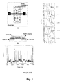
- FIG. 1 shows an example of such passive polydimethylsiloxane (PDMS) biochips with gold electrodes ( L.L. Sohn, O. A. Saleh, G. R. Facer, A. J. Beavis, R. S. Allan, and D. A. Notterman, 'Capacitance cytometry: Measuring biological cells one by one', Proceedings of the National Academy of Siences (USA), Vol. 97, No. 20, September 26, 2000, pp.10687-10690 ).
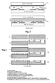
- FIG. 2 shows that this process requires the top covers of the microchannels to be first bonded to a carrier wafer using a low temperature wax. Then, a photosensitive benzocyclobutene, BCB, is spun-on, exposed and developed as to define the sidewalls of the microchannels. Then the photodefined BCB of the carrier wafer is properly aligned and bonded to a receiving wafer integrating the bottoms of the microchannels. Then the wax of the carrier wafer is heated above its melting point as to detach the BCB bonded sidewalls and covers of the carrier wafer onto the bottoms of the receiving wafer, thus creating microchannels.
- BCB photosensitive benzocyclobutene
- FIG. 3 shows that a carrier wafer could be first coated with 1.3um of AZ1813 sacrificial photoresist over which a 0.38um thick layer of parylene could be deposited and patterned as to expose the underlying layer of parylene. Following local etch of the exposed parylene the underlying sacrificial photoresist could be dissolved in acetone as to leave an array of free-standing parylene covers on the carrier wafer.
- the patterned receiving wafer integrating the sidewalls and bottoms of the microchannels could be coated with another layer of 0.38um thick layer of parylene, could be aligned and could be pressed against the free standing pattern of parylene on the carrier wafer while heating at 230°C under a vacuum of 1.5*10 -4 Torr.
- the two parylene layers could polymerize together and will result in bond strength of 3.6 MPa.
- Embodiments of the present invention provide a new, simple, inexpensive, high precision, gold-free, sodium-free and potassium-free process allowing the formation, at a temperature of less than 250°C, of hundreds if not thousands of microfluidics microchannels on a CMOS wafer integrating hundreds if not thousands of digital and/or analog CMOS control logic and/or high voltage CMOS drivers capable of performing sensing and/or microfluidics actuation functions.
- the novel BioMEMS fabrication process uses a layer of silicon nitride exposed to anhydrous hydrofluoric acid as a temporary adhesion layer between a carrier wafer and a multitude of photolithographically defined microfluidics microchannels to be transferred onto the Device Wafer integrating a large number (potentially hundreds or thousands) of digital and/or analog CMOS control logic and/or high voltage CMOS drivers capable of performing sensing and/or microfluidics actuation functions.
- a method of making a MEMS device comprising depositing a silicon nitride layer on a first part; chemically modifying said silicon nitride layer to form a modified surface layer subject to thermal decomposition into gaseous by-products; forming a first structure on said modified surface layer; forming a second structure on a second part; bonding said first and second structures together to form a integrated device; and applying heat to decompose said modified surface layer and thereby separate one of said parts from said bonded structures.
- a method of forming a MEMS device containing microchannels comprising depositing a silicon nitride layer on a carrier wafer; modifying a surface portion of said silicon nitride layer by exposure to anhydrous HF to form a modified surface layer; forming a patterned first structure on said modified surface layer; forming a patterned second structure on a device wafer; bonding said first and second structure together to form microchannels; and releasing said carrier wafer by heating said structures to decompose said modified surface layer.
- Embodiments of the present invention thus provide new, simple, inexpensive, high logic and/or high voltage CMOS drivers capable of performing sensing and/or microfluidics actuation functions in MEMS devices.
- a layer of silicon nitride, Si 3 N 4 to is exposed to an anhydrous hydrofluoric acid, HF.
- This exposure results in the transformation of the silicon nitride layer into a layer of ammonium fluorosilicate, (NH 4 ) 2 SiF 6 , and in the evaporation of silicon tetrafluoride, SiF 4 (g): Si 3 N 4 (s) + 16 HF(g) ⁇ 2(NH 4 ) 2 SiF 6 (s) + SiF 4 (g) ⁇
- Figure 4 shows Secondary Emission Microscopy, SEM, pictures of the chemical attack of silicon nitride by anhydrous HF.
- SEM Secondary Emission Microscopy
- Figure 5 shows the chemical structure of the ammonium fluorosilicate, (NH 4 ) 2 SiF 6 , compound resulting from the chemical attack of silicon nitride by anhydrous HF.
- Ammonium fluorosilicate is also known as ammonium fluorosilicate, ammonium hexafluorosilicate, ammonium silicofluoride, bararite, cryptohalite, cryptophthalite, and diammonium hexafluorosilicate.
- Figure 6 shows the ammonium bifluoride, NH 4 HF 2 (CAS No. 1341-49-7), product resulting from this thermal decomposition.
- Ammonium bifluoride is also known as: acid ammonium fluoride, ammonium acid fluoride, ammoniumbifluoride, ammonium difluoride, ammonium fluoride, ammonium hydrofluoride, ammonium hydrogen bifluoride, ammonium hydrogen difluoride, ammonium hydrogen fluoride, ammonium monohydrogen difluoride, and flammon crystals.
- Figure 7 shows a top view optical pictures of a MEMS device released by removing the sacrificial oxide using the anhydrous HF release process.
- the top picture shows a region located over the etch-stop silicon nitride following exposure to the anhydrous HF release process while the bottom picture shows a region of the same device also located over the etch-stop silicon nitride also following an exposure to the anhydrous HF release process but following an evaporation of the produced ammonium fluorosilicate under nitrogen ambient at a temperature of more than 240°C at atmospheric pressure.
- Figure 8 shows a top view optical picture of the region of the silicon nitride of a MEMS device which had its mechanical structure released by removing the sacrificial oxide using the anhydrous HF release process and which had the ammonium fluorosilicate evaporated under nitrogen ambient at a temperature of more than 240°C at atmospheric pressure.
- the top view optical picture points the region of silicon nitride that has been attacked by the anhydrous HF release process and that has been cleared from its ammonium fluorosilicate following the evaporation under nitrogen ambient at a temperature of more than 240°C at atmospheric pressure.
- the residual surface roughness of this same region is analyzed using white light 3D interferometry nanoimaging as to provide information about the residual topography following the evaporation of the ammonium fluorosilicate, (NH 4 ) 2 SiF 6 .
- the white light 3D interferometry nanoimaging clearly shows a very impressive smooth surface with a residual RMS (Rq) surface roughness of only 1.47nm or about 7 atomic layers.
- Figure 9 estimates that the complete sublimation of ammonium fluorosilicate, (NH 4 ) 2 SiF 6 (g) ⁇ , and ammonium bifluoride, NH 4 HF 2 (g) ⁇ , is possible without liquid phase formation at a pressure of less than the ammonium bifluoride triple point pressure of about 40Torr if the temperature is higher than the ammonium bifluoride sublimation temperature and if the temperature is higher than the ammonium fluorosilicate sublimation temperature: 2(NH 4 ) 2 SiF 6 (s) ⁇ 2SiF 4 (g) ⁇ +2NH 3 (g) ⁇ + 2NH 4 HF 2 (g) ⁇
- Figure 9 shows that an anhydrous HF release process operating at a pressure of less than the ammonium bifluoride triple point pressure of about 40Torr and at the temperature of the highlighted grey zone of Figure 9 could result in a complete sublimation of ammonium fluorosilicate and ammonium bifluoride resulting from the exposure of silicon nitride to anhydrous HF.
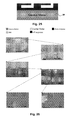
- Figure 10 shows a picture of an array of microchannels produced in accordance with embodiments of the present invention.
- the external surface 14 of the silicon nitride layer 12 is then converted into ammonium fluorosilicate following its exposure to anhydrous HF as shown in Figure 13 Si 3 N 4 (s) + 16 HF(g) ⁇ 2(NH 4 ) 2 SiF 6 (s) + SiF 4 (g)
- the thickness of silicon nitride and the anhydrous HF exposure are such that only a portion of the total thickness of silicon nitride is converted to ammonium fluorosilicate, thus leaving a residual underlayer of silicon nitride 12.
- a 20 ⁇ m thick layer 16 of photopolymer is applied by spinning onto the exposed layer of ammonium fluorosilicate as shown in Figure 14 .
- the thickness of this first layer is adjusted in such a way that it will be strong enough to be used as cover of the microchannel.
- the dried photopolymer is subjected to a pre-exposure bake not exceeding 95°C as to drive-off more of its residual solvents in preparation for the exposure to ultra-violet light through a properly designed mask;
- Figure 15 shows that this 20um thick layer of photopolymer is exposed to ultraviolet light through the openings 18 of a mask 19 defining the shape of the cover of the microchannel.
- the photopolymer Being of negative tone, the photopolymer will reticulate in the regions exposed to the ultraviolet light and will locally become resistant to the chemical attack of the developer to be used later in the process.
- this first layer of a thick negative tone photopolymer is subjected to a post-exposure bake again not exceeding 95°C to drive-off more of the residual solvents and the chemical by-products formed by the ultra-violet light exposure.
- Figure 16 shows that this 20 ⁇ m thick layer of photopolymer is developed, thus defining the cover of the microchannel.
- the regions of the photopolymer that have being exposed to the ultraviolet light passing through the openings of the mask remain intact because resistant to the chemical attack of the developer.
- the resulting photopolymer patterns are subjected to a post-develop bake again not exceeding 95°C as to drive-off more of the residual solvents and the chemical by-products formed by the ultra-violet light exposure and by the develop.
- the developed and baked photopolymer patterns of the carrier wafer are ready to be aligned to the device Wafer;
- Figure 17 shows the silicon wafer used as device wafer substrate 20.
- a 10 ⁇ m thick layer of photopolymer 22 is applied by spinning as shown in Figure 18 . This layer is to become the bottom of the microchannel.
- the dried photopolymer is subjected to a high temperature bake as to drive-off its residual solvents and as to allow the photopolymer to be stabilized i.e. to become chemically stable when an upper layer of photopolymer will be spin-on and exposed in a further step;
- Figure 19 shows that a second layer 24of a 10 ⁇ m thick negative tone photopolymer is applied by spinning onto the exposed first layer 22 of a thick negative tone photopolymer.
- This second layer 24 is to become the sidewall of the microchannel.
- the thickness of this second layer is adjusted in such a way that it will form a tall enough microchannel confined between the already stabilized bottom layer of the Device Wafer and the top layer yet to be transferred from the Carrier Wafer.
- the dried photopolymer is subjected to a pre-exposure bake not exceeding 95°C to drive-off more of its residual solvents in preparation for the exposure to ultra-violet light through a properly designed mask;
- Figure 20 shows that this second layer 24 of a 10 ⁇ m thick negative tone photopolymer is exposed to ultraviolet light through the openings 26 of the mask 28. Being of negative tone, the photopolymer will reticulate in the regions exposed to the ultraviolet light and will locally become resistant to the chemical attack of the developer to be used later in the process. Following ultraviolet light exposure for an optimized dose, this second layer of a thick negative tone photopolymer is subjected to a post-exposure bake again NOT exceeding 95°C to drive-off more solvents and chemical by-products formed by the ultra-violet light exposure;
- Figure 21 shows that this second layer of a properly exposed 10um thick negative tone photopolymer is developed into a proper developer, thus defining the shape of the microchannels 30.
- the regions of the photopolymer that have being exposed to the ultraviolet light passing through the openings of the mask remain intact because they are resistant to the chemical attack of the developer.
- the resulting photopolymer patterns are subjected to a post-develop bake again not exceeding 95°C as to drive-off more of the residual solvents and the chemical by-products formed by the ultra-violet light exposure and by the develop.
- the developed and baked photopolymer patterns of the Device Wafer are ready to be aligned and to receive the transferred top photopolymer layer of the carrier wafer 10.
- Figure 22 shows that the carrier wafer 10 supporting the developed and baked photopolymer patterns defining the cover of the microchannel is flipped-over and properly aligned to the device wafer 20 integrating the sidewall and bottom of the microchannels 30.
- the precise alignment is such that the aligned wafers, not yet in physical contact, are kept in position using a special fixture in preparation for loading of the pair of wafers into a wafer bonding equipment;
- Figure 23 shows that the pair of properly aligned wafers as loaded into the wafer bonding equipment that allows these to become in physical contact by pressing one against the other (without losing alignment accuracy).
- the pair of wafers is then heated, under vacuum, to a temperature not exceeding 95°C while maintaining the two wafers under intimate contact, as to provoke the bonding of the photopolymer of the carrier wafer to the exposed photopolymer of the device wafer 20.
- the pair of wafers is unloaded from the wafer bonding equipment.
- Figure 24 shows the pair of bonded wafers after heating to a temperature exceeding 125°C to decompose the thermally unstable ammonium fluorosilicate, (NH 4 ) 2 SiF 6 (s), of the carrier wafer 10 which provokes the sudden formation and evaporation of volatile silicon tetrafluoride, SiF 4 (g) ⁇ , and volatile ammonia, NH 3 (g) ⁇ , and which results in the formation of a residual ammonium bifluoride, NH 4 HF 2 (s), surface on the carrier wafer: 2(NH 4 ) 2 SiF 6 (s) ⁇ 2SiF 4 (g) ⁇ +2NH 3 (g) ⁇ + 2NH 4 HF 2 (s) and the sublimation of this ammonium bifluoride, NH 4 HF 2 (s), into volatile ammonia, NH 3 (g) ⁇ , and hydrofluoric acid, HF(g) ⁇ .
- This sudden gas formation results in a mechanical release of the carrier wafer from the device wafer that can
- Figure 25 shows the device wafer 20 now incorporating the microchannel heated under vacuum at more than 200°C to chemically stabilize the photopolymer and achieve a solid permanent microchannel.
- Figure 26 shows a series of SEM pictures of a Device Wafer integrating the obtained microchannel. The detailed pictures show that there is a seamless fusion of the bottom, the sidewall and the cover of the microchannel.
- This silicon wafer used as the carrier substrate shown in Figure 11 is preferably a SEMI standard 150mm diameter silicon wafer, but could also, e.g., be a 100mm diameter, a 200mm diameter or a 300mm diameter silicon wafer.
- the silicon nitride, Si 3 N 4 , deposited onto the silicon Carrier Wafer prior to exposure to anhydrous hydrofluoric acid, HF can be conveniently deposited using a Bruce/Kokusai Low Pressure Chemical Vapour Deposition, LPCVD, horizontal furnace such at a preferable temperature of about 830°C, preferably using a mixture of dichlorisilane, SiH 2 Cl 2 and ammonia, NH 3 , as to preferably produce a 0.3um thick layer of silicon nitride.
- This silicon layer could also be deposited at other temperatures ranging from 750°C to 900°C and at other thicknesses ranging from 0.05 um to 1.0um.
- This silicon layer could also be deposited using LPCVD in a vertical LPCVD furnace. This silicon layer could also be deposited at a much lower temperature ranging from 200°C to 500°C with a Plasma Enhanced Chemical Vapour Deposition, PECVD, equipment using mixtures of silane, SiH 4 and ammonia, NH 3 . In that case, the silicon nitride would be a hydrogenated PECVD silicon nitride layer.
- the layer 14 of silicon nitride converted into ammonium fluorosilicate, (NH 4 ) 2 SiF 6 , following its exposure to anhydrous hydrofluoric acid, HF, under a controlled sub-atmospheric pressure of anhydrous HF is preferably 0.1 ⁇ m thick.
- the preferably 0.3 ⁇ m thick initial layer of silicon nitride and the preferable anhydrous HF exposure are such that only the external 0.1 ⁇ m of the preferably 0.3 ⁇ m thick silicon nitride is converted to ammonium fluorosilicate by releasing volatile silicon tetrafluoride, SiF 4 , while leaving a residual underlayer of silicon nitride; Si 3 N 4 (s) + 16 HF(g) ⁇ 2(NH 4 ) 2 SiF 6 (s) + SiF 4 (g) ⁇
- This controlled sub-atmospheric conversion process using anhydrous HF is performed at preferably 70 Torr of anhydrous HF in a Primaxx specialized anhydrous HF processor. Following this surface conversion, the anhydrous HF is stopped and the wafers are exposed to nitrogen ambient before being manipulated under atmospheric conditions to the next step of the process.
- This silicon nitride layer could also be converted in other known types of equipment suitable for this purpose. This silicon nitride layer could also be converted at a pressure ranging between 10 and 750 Torr.
- This silicon nitride layer could also be converted in gas mixtures involving anhydrous HF and an organic volatile, such as: methanol, acetone, 1-buthanol, 2-buthanol, 1-propanol or 2-propanol.
- this silicon nitride layer could also be converted in gas mixtures involving anhydrous HF, nitrogen and solvents or alcohols such as methanol, acetone, 1-buthanol, 2-buthanol, 1-propanol or 2-propanol.
- the thick layer of a negative tone photopolymer 16 shown in Figure 14 is preferably 20 ⁇ m thick and applied by spinning onto the exposed layer of ammonium fluorosilicate.
- a preferred photopolymer is SU-8, a negative tone epoxy-like near-UV photoresist originally developed, and described in US patent No. 4,882,245 entitled: 'Photoresist Composition and Printed Ciruit Boards and Packages Made Therewith'
- This high performance photopolymer is available from three companies: MicroChem Corporation, a company previously named Microlithography Chemical Corporation, of Newton, MA, USA.
- the photopolymer is sold under the name NANO SU-8 at different viscosities: SU-8 2005; SU-8 2010; SU-8 2025; SU-8 2050; SU-8 2100; Gerstel Ltd, a company previously named SOTEC Microsystems, of Pully, Switzerland.
- the photopolymer is sold under the name GM or GLM at different viscosities: GM1040; GM1060; GM1070, GLM2060, GLM3060; and Kayaku Microchem Corporation (KMCC), of Chiyoda-Ku, Tokyo, Japan.
- the photopolymer is sold under the name XP KMPR-1000 SU8 at different viscosities: XP KMPR-1 005; XP KMPR-1010; XP KMPR-1025; XP KMPR-1050; XP KMPR-1100;
- This high performance photopolymer can be spin coated using one of the two coat stations of an EV Group Hercules processor.
- About 3ml of Microchem SU-8 2025 photopolymer solution is dispensed above the 150mm wafer before spinning at about 1600 RPM as to dry the spin-on photopolymer by partial solvents evaporation and as to achieve a film thickness of preferably 20um to be strong enough to become the protection capsule.
- the dried photopolymer is subjected to a pre-exposure bake not exceeding 95°C and for about 8 to 10 minutes as to drive-off more of its residual solvents.
- This MicroChem SU-8 2025 negative tone photopolymer can alternately be replaced by the Gerstel GM 1060 or GLM2060 negative tone photopolymer or by the Kayaku Microchem XP KMPR 1025 negative tone photopolymer to achieve the same preferred thickness of 20um.
- the viscosity of the photopolymer solution could be lower then the one of the Microchem SU-8 2025 photopolymer solution as to reduce the thickness of this first layer of negative tone photopolymer from 40um down to about 5um.
- the Microchem SU-8 2005 or SU-8 2010 negative tone photopolymer solution could be used, the Gerstel GM 1040 negative tone photopolymer solution could be used, or the Kayaku Microchem XP KMPR 1005 or XP KMPR-1010 negative tone photopolymer solution could be used.
- the viscosity of the photopolymer solution could be higher then the one of the Microchem SU-8 2025 photopolymer solution as to increase the thickness of this first layer of negative tone photopolymer from 20um up to about 500um.
- the Microchem SU-8 2050 or SU-8 2100 negative tone photopolymer solution could be used, the Gerstel GM 1070 negative tone photopolymer solution could be used, or the Kayaku Microchem XP KMPR 1050 or XP KMPR-1100 negative tone photopolymer solution could be used.
- To thicker negative tone photopolymer layers should be associated a longer than 90 seconds pre-exposure bake but still not exceeding 95°C and for about as to drive-off the residual solvents.
- the preferably 20um thick layer of negative tone photopolymer is exposed, a shown in Figure 15 , using a highly collimated broadband UV source (g-line, h-line and l-line) of the EV Group Hercules processor through the openings of the mask defining the shape of the protection capsule.
- a highly collimated broadband UV source g-line, h-line and l-line
- the photopolymer will reticulate in the regions exposed to the ultraviolet light and will locally become resistant to the chemical attack of the developer to be used later in the process.
- this first layer of a thick negative tone photopolymer is subjected to a 5 minutes duration post-exposure bake again not exceeding 95°C as to drive-off more of the residual solvents and the chemical by-products formed by the ultra-violet light exposure. At this point, the exposed photopolymer is not yet developed.
- MicroChem SU-8 2025, Gerstel GM 1060 or GLM2060 or Kayaku Microchem XP KMPR 1025 negative tone photopolymer is replaced by a lower viscosity solution such as the Microchem SU-8 2005 or SU-8 2010, the Gerstel GM 1040 or the Kayaku Microchem XP KMPR 1005 or XP KMPR-1010 negative tone photopolymer solution, then the optimized dose would be lower than about 310mJ/cm 2 , to prevent over-exposure of this first layer of a negative tone photopolymer.
- MicroChem SU-8 2025, Gerstel GM 1060 or GM 2060 or Kayaku Microchem XP KMPR 1025 negative tone photopolymer is replaced by a higher viscosity solution such as the Microchem SU-8 2050 or SU-8 2100, the Gerstel GM 1070 or the Kayaku Microchem XP KMPR 1050 or XP KMPR-1100 negative tone photopolymer solution, then the optimized dose would be higher than about 310mJ/cm 2 , to prevent under-exposure of this first layer of a negative tone photopolymer. Thicker negative tone photopolymer layers are associated with a longer than 90 seconds post-exposure bake but still not exceeding 95°C.
- the preferably 20 ⁇ m thick layer of MicroChem SU-8 2025 negative tone photopolymer is developed using one of the two develop stations of the EV Group Hercules processor to define an array of covers to be transferred onto the array of microchannels of another substrate.
- the regions of the photopolymer that have been exposed to the ultraviolet light passing through the openings of the mask remain intact because resistant to the chemical attack of the developer.
- This layer of negative tone photopolymers is capable of achieving complex structures and mechanical features having a height:width aspect ratio as high as 10:1.
- Figure 17 shows the silicon wafer used as the device wafer substrate 20.
- This silicon wafer is preferably a SEMI standard 150mm diameter silicon wafer but could also, for example, be a 100mm diameter, a 200mm diameter or a 300mm diameter silicon wafer;
- Figure 18 shows that a first layer of a preferably 10um thick layer negative tone photopolymer applied by spinning.
- This first layer is to become an array of bottoms of the array of microchannels.
- This negative tone photopolymer is spin coated using one of the two coat stations of the EV Group Hercules processor. Again, about 3ml of Microchem SU-8 2005 is dispensed above the 150mm wafer before spinning at about 1600 RPM to dry the spin-on photopolymer by partial solvents evaporation and to achieve a film thickness of preferably 10 ⁇ m.
- the dried photopolymer is subjected to a pre-exposure bake not exceeding 95°C and for about 5 minutes as to drive-off more of its residual solvents.
- This MicroChem SU-8 2005 negative tone photopolymer can alternately be replaced by the MicroChem SU-8 2010, the Gerstel GM 1040 or the Kayaku Microchem XP KMPR 1005 or XP KMPR 1010 negative tone photopolymer to achieve the same preferred thickness of 10 ⁇ m.
- the viscosity of the photopolymer solution could be higher than the one of the MicroChem SU-8 2005 photopolymer solution to increase its thickness above 10 ⁇ m.
- the Microchem SU-8 2025 or SU-8 2050 or SU-8 2100, the Gerstel GM 1060, GM 1070 or GM 2060 or the Kayaku Microchem XP KMPR 1025, XP KMPR 1050 or XP KMPR-1100 negative tone photopolymer solution could be used.
- thicker negative tone photopolymer layers should be associated with a longer than 90 seconds pre-exposure bake at about 95°C to drive-off more of the residual solvents.
- a vacuum bake at a temperature of about 180°C is performed for about 2 hours to stabilize this first 10um thick layer and prevent its photochemical activity when exposed to ultra-violet light.
- the second layer 24 of a preferably 10um thick negative tone photopolymer shown in Figure 19 is applied by spinning onto the thermally stabilized 10um thick negative tone photopolymer. Again, this high performance photopolymer is spin coated using one of the two coat stations of the EV Group Hercules processors. Again, about 3ml of Microchem SU-8 2005 is dispensed above the 150mm wafer before spinning at about 1600 RPM as to dry the spin-on photopolymer by partial solvents evaporation and as to achieve a 10um thick film. The dried photopolymer is subjected to a pre-exposure bake not exceeding 95°C and for about 5 minutes as to drive-off more of its residual solvents.
- This MicroChem SU-8 2005 negative tone photopolymer can alternately be replaced by the MicroChem SU-8 2010, the Gerstel GM 1040 or the Kayaku Microchem XP KMPR 1005 or XP KMPR 1010 negative tone photopolymer to achieve the same preferred thickness of 10 ⁇ m.
- the viscosity of the photopolymer solution could be higher than the one of the MicroChem SU-8 2005 photopolymer solution to increase its thickness above 10 ⁇ m.
- the Microchem SU-8 2025 or SU-8 2050 or SU-8 2100, the Gerstel GM 1060, GM 1070 or GM 2060 or the Kayaku Microchem XP KMPR 1025, XP KMPR 1050 or XP KMPR-1100 negative tone photopolymer solution could be used.
- to thicker negative tone photopolymer layers should be associated a longer than 90 seconds pre-exposure bake but still not exceeding 95°C and for about as to drive-off more of its residual solvents in preparation for the exposure to ultra-violet light through a properly designed mask.
- This second layer of a preferably 10um thick MicroChem SU-8 2005 negative tone photopolymer is exposed, as shown in Figure 20 , using the highly collimated broadband UV source (g-line, h-line and I-line) of the EV Group Hercules processor through the openings of the mask defining the array of sidewalls of the array of microchannels. Being of negative tone, the photopolymer will reticulate in the regions exposed to the ultraviolet light and will locally become resistant to the chemical attack of the developer to be used later in the process.
- the highly collimated broadband UV source g-line, h-line and I-line
- this first layer of a thick negative tone photopolymer is subjected to a 3 minutes duration post-exposure bake again not exceeding 95°C as to drive-off more of the residual solvents and the chemical by-products formed by the ultra-violet light exposure.
- This second layer of a preferably 10 ⁇ m thick MicroChem SU-8 2005 negative tone photopolymer is developed, a shown in Figure 16 , using one of the two develop stations of the EV Group Hercules processor to define the defining the array of sidewalls of the array of microchannels.
- the regions of the photopolymer that have being exposed to the ultraviolet light passing through the openings of one or both of the masks remain intact because resistant to the chemical attack of the developer.
- These two layers of negative tone photopolymers are capable of achieving complex structures and mechanical features having a height:width aspect ratio as high as 10:1.
- the resulting photopolymer patterns are subjected to a post-develop bake at about 95°C as to drive-off more of the residual solvents and the chemical by-products formed by the ultra-violet light exposure and by the develop.
- a vacuum bake at a temperature of about 180°C is performed for about 2 hours to stabilize this exposed second 10um thick layer.
- the developed and baked photopolymer patterns of the Device Wafer are ready to be aligned and to receive the transferred top photopolymer layer of the Carrier Wafer.
- the carrier wafer 10 supporting the developed and baked photopolymer patterns defining the array of covers of the array of microchannels is flipped-over, as shown in Figure 22 , and properly aligned to the Device Wafer integrating the array of sidewalls and the array of bottoms of the array of microchannels using a SmartView aligner of the EV Group Gemini processor.
- the alignment is precise within about 1 ⁇ m.
- the aligned wafers, not yet in physical contact, are kept in position using a special fixture in preparation for loading of the pair of wafers into one of the four Universal bond chamber of the EV Group Gemini processor.
- the pair of properly aligned wafers are loaded into one of the four Universal bond chamber of the EV Group Gemini processor.
- This Universal bond chamber allows the carrier wafer and the device wafer to become in physical contact by slowly pressing one against the other (without losing alignment accuracy) with a uniform force of 5kN to 20kN while heating the two wafers at a temperature not exceeding 95°C for about 20 minutes as to provoke the permanent bonding of the photopolymer of the carrier wafer to the exposed top bond material of the Device Wafer.
- the precise alignment of about 1 ⁇ m achieved with the SmartView is such that the thousands of protection capsules of the carrier wafer do not make a direct contact to the thousands of free-to-move mechanical devices of the device wafer during this bonding process.
- the bonded pair of wafers is unloaded from the universal bond chamber, cooled-down to room temperature using a cool station and returned in a properly designed receiving cassette.
- the pair of bonded wafers is heated to a temperature exceeding 125°C to decompose the thermally unstable ammonium fluorosilicate, (NH 4 ) 2 SiF 6 (s), of the carrier wafer which provokes the sudden formation and evaporation of volatile silicon tetrafluoride, SiF 4 (g) ⁇ , and volatile ammonia, NH 3 (g) ⁇ , and which results in the formation of a residual ammonium bifluoride, NH 4 HF 2 (s), surface on the carrier wafer: 2(NH 4 ) 2 SiF 6 (s) ⁇ 2SiF 4 (g) ⁇ +2NH 3 (g) ⁇ + 2NH 4 HF 2 (s) and the sublimation of this ammonium bifluoride, NH 4 HF 2 (s), into volatile ammonia, NH 3 (g) ⁇ , and hydrofluoric acid, HF(g) ⁇ .
- This sudden gas formation results in a mechanical release of the carrier wafer from the device wafer that can now be separated at
- Embodiments of the present invention thus provide a simple, inexpensive, high precision, gold-free, sodium-free and potassium-free process allowing the formation, at a temperature of less than 250°C, of hundreds if not thousands of microfluidics microchannels on a CMOS wafer integrating hundreds if not thousands of digital and/or analog CMOS control logic and/or high voltage CMOS drivers capable of performing sensing and/or microfluidics actuation functions.
- the carrier wafer may be a silicon carrier wafer, a glass carrier wafer, a compound semiconductor carrier wafer, a ceramic carrier wafer, or a metal carrier wafer.
- the silicon nitride may be deposited by Low Pressure Chemical Vapour Deposition, LPCVD in a horizontal or vertical furnace at a temperature ranging from 750°C to 900°C, preferably about 830°C.
- the LPCVD silicon nitride may be deposited using a mixture of dichlorisilane, SiH 2 Cl 2 and ammonia, NH 3 at a thickness ranging from 0.05 ⁇ m to 1.0 ⁇ m, preferably about 0.3 ⁇ m.
- the silicon nitride could also be deposited by Plasma Enhanced Chemical Vapour Deposition, PECVD in either batch equipment or single wafer equipment at a temperature ranging from 200°C to 500°C, preferably about 400°C using a mixture of silane, SiH 4 and ammonia, NH 3 .
- the PECVD silicon nitride is deposited at a thickness ranging from 0.05 ⁇ m to 1.0 ⁇ m, preferably about 0.3um.
- the anhydrous HF process is preferably performed in a sub-atmospheric pressure of anhydrous HF at a pressure ranging from 10 to 750 Torr, preferably about 70 Torr, in a mixture of anhydrous HF and an organic volatile, such as methanol, acetone, 1-buthanol, 2-buthanol, 1-propanol or 2-propanol.
- an organic volatile such as methanol, acetone, 1-buthanol, 2-buthanol, 1-propanol or 2-propanol.
- the broadband UV source used to expose the polymers should be highly collimated to achieve high aspect ratio features.
- the second exposed and heat treated photopolymer can be developed to form a spacer ring for the device, or the first and second exposed and heat treated photopolymers can be developed together as to simultaneously form a protection capsule underlying a spacer ring.
- the device wafer may contain CMOS devices.
- the bonding of the structures can be performed by applying a force from 5kN to 20kN.
- the applied force of 5kN to 20kN should be applied to the effective surface area of the full 150mm wafers (175 cm 2 ), thus resulting in an effective applied pressure of 0.5MPa to 1.1 MPa.
- the applied force of 5kN to 20kN should be applied to the effective surface area of the thousands of protection capsules, representing about 20% of the area of the full 150mm wafers (35 cm 2 ), thus resulting in an effective applied pressure of 1.4MPa to 7MPa.
- the applied force of 5kN to 20kN should be applied to the effective surface area of the thousands of sidewalls underneath the thousands of covers, representing about 4% of the area of the full 150mm wafers (7.0 cm 2 ), thus resulting in an effective applied pressure of 6.7MPa to 29MPa.
- the heating of the wafers should be performed for about 20 minutes to produce a permanent bond between the contacted photopolymer of the carrier wafer to the exposed top bond material of the device wafer.
- the separation of the wafers may take place outside the vacuum environment at a temperature exceeding 125°C.
- the separated device wafer may be exposed to a vacuum lower than 100 Pa at a temperature of up to 200°C for up to four hours to polymerize the formed microchannels and convert them into hard and very adherent epoxy-like microchannels.
Abstract


Description
- This invention relates to micro-electromechanical systems (MEMS) devices, and in particular, but not exclusively, to a method of fabricating microchannels in such devices for use in biololigical applications.
- Various techniques for fabricating microchannels in BIOMEMS devices are known in the prior art. Such techniques are described in the following patent applications:
US Patent No. 6,186,660 « Microfluidic systems incorporating varied channel dimensions »;US Patent No. 6,180,536 «Suspended moving channels and channel actuators for ...»;US Patent No. 6,174,675 « Electrical current for controlling fluid parameters in ...»;US Patent No. 6,172,353 « System and method for measuring low power signals »;US Patent No. 6,171,865 « Simultaneous analyte determination and reference ...»;US Patent No. 6,171,850 « Integrated devices and systems for performing ...»;US Patent No. 6,171,067 « Micropump »;US Patent No. 6,170,981 « In situ micromachined mixer for microfluidic analytical ...»;US Patent No. 6,167,910 « Multi-layer microfluidic devices »;US Patent No. 6,159,739 « Device and method for 3-dimensional alignment of ...»;US Patent No. 6,156,181 « Controlled fluid transport microfabricated polymeric ... »;US Patent No. 6,154,226 « Parallel print array »;US Patent No. 6,153,073 « Microfluidic devices incorporating improved channel ...»;US Patent No. 6,150,180 « High throughput screening assay systems in ...»;US Patent No. 6,150,119 « Optimized high-throughput analytical system »;US Patent No. 6,149,870 « Apparatus for in situ concentration and/or dilution of ...»;US Patent No. 6,149,787 « External material accession systems and methods »;US Patent No. 6,148,508 « Method of making a capillary for electrokinetic ...»;US Patent No. 6,146,103 « Micromachined magnetohydrodynamic actuators ... »;US Patent No. 6,143,248 « Capillary microvalve »;US Patent No. 6,143,152 « Microfabricated capillary array electrophoresis device ...»;US Patent No. 6,137,501 « Addressing circuitry for microfluidic printing apparatus »;US Patent No. 6,136,272 « Device for rapidly joining and splitting fluid layers »;US Patent No. 6,136,212 « Polymer-based micromachining for microfluidic devices »;US Patent No. 6,132,685 « High throughput microfluidic systems and methods »;US Patent No. 6,131,410 « Vacuum fusion bonding of glass plates »;US Patent No. 6,130,098 « Moving microdroplets »;US Patent No. 6,129,854 « Low temperature material bonding technique »;US Patent No. 6,129,826 « Methods and systems for enhanced fluid transport »;US Patent No. 6,126,765 « Method of producing microchannel/microcavity ...»;US Patent No. 6,126,140 « Monolithic bi-directional microvalve with enclosed...»;US Patent No. 6,123,798 « Methods of fabricating polymeric structures ...»;US Patent No. 6,120,666 « Microfabricated device and method for multiplexed ...»;US Patent No. 6,118,126 « Method for enhancing fluorescence »;US Patent No. 6,107,044 « Apparatus and methods for sequencing nucleic ...»;US Patent No. 6,106,685 « Electrode combinations for pumping fluids »;US Patent No. 6,103,199 « Capillary electroflow apparatus and method »;US Patent No. 6,100,541 « Microfluidic devices and systems incorporating ... »;US Patent No. 6,096,656 « Formation of microchannels from low-temperature ... »;US Patent No. 6,091,502 « Device and method for performing spectral ...»;US Patent No. 6,090,251 « Microfabricated structures for facilitating fluid ...»;US Patent No. 6,086,825 « Microfabricated structures for facilitating fluid ...»;US Patent No. 6,086,740 « Multiplexed microfluidic devices and systems »;US Patent No. 6,082,140 « Fusion bonding and alignment fixture »;US Patent No. 6,080,295 « Electropipettor and compensation means for ...»;US Patent No. 6,078,340 « Using silver salts and reducing reagents in ... »;US Patent No. 6,074,827 « Microfluidic method for nucleic acid purification and ... »;US Patent No. 6,074,725 « Fabrication of microfluidic circuits by printing techniques »;US Patent No. 6,073,482 « Fluid flow module »;US Patent No. 6,071,478 « Analytical system and method »;US Patent No. 6,068,752 « Microfluidic devices incorporating improved channel ...»;US Patent No. 6,063,589 « Devices and methods for using centripetal ...»;US Patent No. 6,062,261 « Microfluldic circuit designs for performing ...»;US Patent No. 6,057,149 « Microscale devices and reactions in microscale devices »;US Patent No. 6,056,269 « Microminiature valve having silicon diaphragm »;US Patent No. 6,054,277 « Integrated microchip genetic testing system »;US Patent No. 6,048,734 « Thermal microvalves in a fluid flow method »;US Patent No. 6,048,498 « Microfluidic devices and systems »;US Patent No. 6,046,056 « High throughput screening assay systems in ...»;US Patent No. 6,043,080 « Integrated nucleic acid diagnostic device »;US Patent No. 6,042,710 « Methods and compositions for performing molecular »;US Patent No. 6,042,709 « Microfluidic sampling system and methods »;US Patent No. 6,012,902 « Micropump »;US Patent No. 6,011,252 « Method and apparatus for detecting low light levels »;US Patent No. 6,007,775 « Multiple analyte diffusion based chemical sensor »;US Patent No. 6,004,515 « Methods and apparatus for in situ concentration ... »;US Patent No. 6,001,231 « Methods and systems for monitoring and controlling ...»;US Patent No. 5,992,820 « Flow control in microfluidics devices by controlled ...»;US Patent No. 5,989,402 « Controller/detector interfaces for microfluidic systems »;US Patent No. 5,980,719 « Electrohydrodynamic receptor »;US Patent No. 5,972,710 « Microfabricated diffusion-based chemical sensor »;US Patent No. 5,972,187 « Electropipettor and compensation means for ... »;US Patent No. 5,965,410 « Electrical current for controlling fluid parameters in ...»;US Patent No. 5,965,001 « Variable control of electroosmotic and/or ...»;US Patent No. 5,964,995 « Methods and systems for enhanced fluid transport »;US Patent No. 5,958,694 « Apparatus and methods for sequencing nucleic acids ...»;US Patent No. 5,958,203 « Electropipettor and compensation means for ... »;US Patent No. 5,957,579 « Microfluidic systems incorporating varied channel ... »;US Patent No. 5,955,028 « Analytical system and method »;US Patent No. 5,948,684 « Simultaneous analyte determination and reference ...»;US Patent No. 5,948,227 « Methods and systems for performing electrophoretic ...»;US Patent No. 5,942,443 « High throughput screening assay systems in ...»;US Patent No. 5,932,315 « Microfluidic structure assembly with mating ... »;US Patent No. 5,932,100 « Microfabricated differential extraction device and ...»;US Patent No. 5,922,604 « Thin reaction chambers for containing and handling ...»;US Patent No. 5,922,210 « Tangential flow planar microfabricated fluid filter and ...»;US Patent No. 5,885,470 « Controlled fluid transport in microfabricated polymeric ...»;US Patent No. 5,882,465 « Method of manufacturing microfluidic devices »;US Patent No. 5,880,071 « Electropipettor and compensation means for ... »;US Patent No. 5,876,675 « Microfluidic devices and systems »;US Patent No. 5,869,004 « Methods and apparatus for in situ concentration ... »;US Patent No. 5,863,502 « Parallel reaction cassette and associated devices »;US Patent No. 5,856,174 « Integrated nucleic acid diagnostic device »;US Patent No. 5,855,801 « IC-processed microneedles »;US Patent No. 5,852,495 « Fourier detection of species migrating in a ... »;US Patent No. 5,849,208 « Making apparatus for conducting biochemical analyses »;US Patent No. 5,842,787 «Microfluidic systems incorporating varied channel ... »;US Patent No. 5,800,690 « Variable control of electroosmotic and/or ... »;US Patent No. 5,779,868 « Electropipettor and compensation means for ... »;US Patent No. 5,755,942 « Partitioned microelectronic device array »;US Patent No. 5,716,852 « Microfabricated diffusion-based chemical sensor »;US Patent No. 5,705,018 « Micromachined peristaltic pump »;US Patent No. 5,699,157 « Fourier detection of species migrating in a ... »;US Patent No. 5,591,139 «IC-processed microneedles»; andUS Patent No. 5,376,252 «Microfluidic structure and process for its manufacture». - The paper by L. L. Sohn, O. A. Saleh, G. R. Facer, A. J. Beavis, R. S. Allan, and D. A. Notterman, 'Capacitance cytometry: Measuring biological cells one by one', Proceedings of the National Academy of Siences (USA), Vol. 97, No. 20, September 26, 2000, pp.10687-10690 discloses a polydimethylsiloxane (PDMS) biochip capable of capacitance detection of biological entities (mouse cells).
- This prior art shows that passive micro-channel biochip devices are fabricated using fusion bonding of a combination of various substrates, such as: acrylonitrile-butadiene-styrene copolymer, polycarbonate, polydimethylsiloxane (PDMS), polyethylene, polymethylmethacrylate (PMMA), polymethylpentene, polypropylene, polystyrene, polysulfone, polytetrafluoroethylene (PTFE), polyurethane, polyvinylchloride (PVC), polyvinylidine fluoride (PVF). These Prior Art USA Patents show that mechanical stamping or thermal forming techniques are used to define a network of micro-channels in a first substrate prior its fusion bonding to another such substrate, as to form microchannels between the two bonded substrates. The result is a simple passive micro-channel biochip device which can be patterned with conductive layers as to connect an external processor used to provoke fluid movement by electrophoresis or electroosmosis, analysis and data generation. An example of such passive micro-channel biochip devices obtained from the fusion of such polymeric substrates is shown in
US Patent No. 6,167,910 « Multi-layer microfluidic devices ». - The Prior Art also indicates that passive micro-channel biochip devices can be fabricated from the combination of various micro-machined silica or quartz substrates. Again, assembly and fusion bonding is required. The result is again a simple passive biochip device which can be patterned with conductive layers as to connect an external processor used to provoke fluid movement by electrophoresis or electroosmosis, analysis and data generation. An example of such passive micro-channel biochip devices obtained from the fusion of such silica substrates is shown in
US Patent No. 6,131,410 «Vacuum fusion bonding of glass plates ». - The cited US Patents also indicate that passive micro-channel biochip devices can be fabricated from a passive micro-machined silicon substrate. In that case, the silicon substrate is used as a passive structural material. Again, assembly and fusion bonding of at least two sub-assemblies is required. The result is again a simple passive biochip to connect to an external processor used to provoke fluid movement, analysis and data generation. An example of such passive micro-channel biochip devices obtained from a passive micro-machined silicon substrate is shown in
US Patent No. 5,705,018 « Micromachined peristaltic pump ». - The cited US Patents also indicate that active micro-reservoir biochip devices can be fabricated from machining directly into an active silicon substrate. In that case, the control electronics integrated in the silicon substrate is used as an active on-chip fluid processor and communication device. The result is a sophisticated biochip device which can perform, into pre-defined reservoirs, various fluidics, analysis and (remote) data communication functions without the need of an external fluid processor in charge of fluid movement, analysis and data generation. An example of such active micro-reservoir biochip devices obtained from an active micro-machined silicon substrate is shown in
US Patent No. 6,117,643 « Bioluminescent bioreporter integrated circuit ». - These Prior Art references also indicate that passive polydimethylsiloxane (PDMS) biochips have been developed for the detection of biological entities using gold coated capacitor electrodes.
Figure 1 shows an example of such passive polydimethylsiloxane (PDMS) biochips with gold electrodes (L.L. Sohn, O. A. Saleh, G. R. Facer, A. J. Beavis, R. S. Allan, and D. A. Notterman, 'Capacitance cytometry: Measuring biological cells one by one', Proceedings of the National Academy of Siences (USA), Vol. 97, No. 20, September 26, 2000, pp.10687-10690). - These Prior Art references also indicate that wax has been used to fabricate such microchannels.
Figure 2 shows that this process requires the top covers of the microchannels to be first bonded to a carrier wafer using a low temperature wax. Then, a photosensitive benzocyclobutene, BCB, is spun-on, exposed and developed as to define the sidewalls of the microchannels. Then the photodefined BCB of the carrier wafer is properly aligned and bonded to a receiving wafer integrating the bottoms of the microchannels. Then the wax of the carrier wafer is heated above its melting point as to detach the BCB bonded sidewalls and covers of the carrier wafer onto the bottoms of the receiving wafer, thus creating microchannels. An example of such an approach in shown in the paper by A. Jourdain, X. Rottenberg, G. Carchon and H.A.C. Tilmanstitled, 'Optimization of 0-Level Packaging for RF-MEMS Devices', Transducers 2003, The 12th International Conference on Solid State Sensors, Actuators and Microsystems, Boston, June 8-12, 2003, pp. 1915-1918 - These Prior Art references also indicate that parylene could be used to fabricate such microchannels.
Figure 3 shows that a carrier wafer could be first coated with 1.3um of AZ1813 sacrificial photoresist over which a 0.38um thick layer of parylene could be deposited and patterned as to expose the underlying layer of parylene. Following local etch of the exposed parylene the underlying sacrificial photoresist could be dissolved in acetone as to leave an array of free-standing parylene covers on the carrier wafer. The patterned receiving wafer integrating the sidewalls and bottoms of the microchannels could be coated with another layer of 0.38um thick layer of parylene, could be aligned and could be pressed against the free standing pattern of parylene on the carrier wafer while heating at 230°C under a vacuum of 1.5*10-4 Torr. The two parylene layers could polymerize together and will result in bond strength of 3.6 MPa. An example of such an approach in shown in the paper by H.S. Kim and K. Najafi, 'Wafer Bonding Using Parylene and Wafer-Level Transfer of Free-Standing Parylene Membranes', Transducers 2003, The 12th International Conference on Solid State Sensors, Actuators and Microsystems, Boston, June 8-12, 2003, pp. 790-793. - Embodiments of the present invention provide a new, simple, inexpensive, high precision, gold-free, sodium-free and potassium-free process allowing the formation, at a temperature of less than 250°C, of hundreds if not thousands of microfluidics microchannels on a CMOS wafer integrating hundreds if not thousands of digital and/or analog CMOS control logic and/or high voltage CMOS drivers capable of performing sensing and/or microfluidics actuation functions. The novel BioMEMS fabrication process uses a layer of silicon nitride exposed to anhydrous hydrofluoric acid as a temporary adhesion layer between a carrier wafer and a multitude of photolithographically defined microfluidics microchannels to be transferred onto the Device Wafer integrating a large number (potentially hundreds or thousands) of digital and/or analog CMOS control logic and/or high voltage CMOS drivers capable of performing sensing and/or microfluidics actuation functions.
- Thus in accordance with a first aspect of the invention there is provided a method of making a MEMS device, comprising depositing a silicon nitride layer on a first part; chemically modifying said silicon nitride layer to form a modified surface layer subject to thermal decomposition into gaseous by-products; forming a first structure on said modified surface layer; forming a second structure on a second part; bonding said first and second structures together to form a integrated device; and applying heat to decompose said modified surface layer and thereby separate one of said parts from said bonded structures.
- According to a second aspect of the invention there is provided a method of forming a MEMS device containing microchannels, comprising depositing a silicon nitride layer on a carrier wafer; modifying a surface portion of said silicon nitride layer by exposure to anhydrous HF to form a modified surface layer; forming a patterned first structure on said modified surface layer; forming a patterned second structure on a device wafer; bonding said first and second structure together to form microchannels; and releasing said carrier wafer by heating said structures to decompose said modified surface layer.
- Embodiments of the present invention thus provide new, simple, inexpensive, high logic and/or high voltage CMOS drivers capable of performing sensing and/or microfluidics actuation functions in MEMS devices.
- The present invention will be described in more detail, by way of example only, with reference to the accompanying drawings, in which:-
-
Figure 1 shows an example of passive polydmethylsiloxane biochips with gold electrodes; -
Figure 2 shows a form of O-level packaging for RF MEMS devices; -
Figure 3 shows the transfer of free-standing parylene membranes; -
Figure 4 shows Secondary Emission Microscopy, SEM, pictures of the chemical attack of silicon nitride by anhydrous HF; -
Figure 5 shows the chemical structure of the ammonium fluorosilicate, (NH4)2SiF6, compound resulting from the chemical attack of silicon nitride by anhydrous HF; -
Figure 6 shows the ammonium bifluoride, NH4HF2 (CAS No. 1341-49-7), product resulting from this thermal decomposition; -
Figure 7 shows the top view optical pictures of a MEMS device released by removing the sacrificial oxide using the anhydrous HF release process; -
Figure 8 shows a top view optical picture of the region of the silicon nitride of a MEMS device which had its mechanical structure released by removing the sacrificial oxide using the anhydrous HF release process; -
Figure 9 is a sketch of the ammonium bifluoride phase diagram proposed by B. Du Bois (IMEC, 1999); -
Figure 10 shows arrays of microchannels produced by the present invention; -
Figure 11 shows the silicon wafer used as Carrier Wafer substrate; -
Figure 12 shows the silicon nitride deposited onto the Carrier Wafer prior to exposure to anhydrous HF; -
Figure 13 shows the chemical conversion of the external surface of silicon nitride into ammonium fluorosilicate following its exposure to anhydrous HF; -
Figure 14 shows a 20µm thick layer of photopolymer applied by spinning onto the exposed layer of ammonium fluorosilicate; -
Figure 15 shows this 20um thick layer of photopolymer exposed to ultraviolet light through the openings of the mask defining the shape of the cover of the microchannel; -
Figure 16 shows this 20um thick layer of photopolymer developed, thus defining the cover of the microchannel; -
Figure 17 shows the silicon wafer used as device wafer substrate; -
Figure 18 shows a 10um thick layer of photopolymer applied by spinning; -
Figure 19 shows a second layer of a 10um thick negative tone photopolymer applied by spinning onto the exposed first layer of a thick negative tone photopolymer; -
Figure 20 shows this second layer of 10um thick negative tone photopolymer exposed to ultraviolet light through the openings of the mask; -
Figure 21 shows this second layer of a properly exposed 10um thick negative tone photopolymer developed into a proper developer, thus defining the shape of the microchannels; -
Figure 22 shows that the carrier wafer supporting the developed and baked photopolymer patterns defining the cover of the microchannel flipped-over and properly aligned to the Device Wafer integrating the sidewall and bottom of the microchannel; -
Figure 23 shows the pair of properly aligned wafers that loaded into the wafer bonding equipment; -
Figure 24 shows the pair of bonded wafers heated to a temperature exceeding 125°C as to decompose the thermally unstable ammonium fluorosilicate; -
Figure 25 shows that the device wafer now incorporating the microchannel heated under vacuum at more then 200°C to chemically stabilize the photopolymer and to achieve a solid permanent microchannel; and -
Figure 26 shows a series of SEM pictures of a Device Wafer integrating the obtained microchannel. - In accordance with embodiments of the invention a layer of silicon nitride, Si3N4, to is exposed to an anhydrous hydrofluoric acid, HF. This exposure results in the transformation of the silicon nitride layer into a layer of ammonium fluorosilicate, (NH4)2SiF6, and in the evaporation of silicon tetrafluoride, SiF4(g):
Si3N4(s) + 16 HF(g) → 2(NH4)2SiF6(s) + SiF4(g)↑
- The following documents are cited as references to this anhydrous HF process typically used for the stiction-free release of advanced MEMS devices integrating sensitive mechanical parts prone to stiction: R.S. Blackwood, R. L. Biggerstaff, L. D. Clements, R. Cleavelin, "Gaseous Process and Apparatus for Removing Films from Substrates", USA Patent
4,749,440, June 7,1988 ; J. Ruzyllo, K. Torek, C. Draffon, R. Grant, R. Novak, "Etching of Thermal Oxides in Low Pressure Anhydrous HF/CH3OH Gas Mixtures at Elevated Temperatures", J. Electrochem Soc., Vol. 140, No. 4, April 1993, pp. L64-L66;US Patent No. 5,439,553 , "Controlled Etching of Oxides via Gas Phase reactions", August 8,1995; K. Torek, J. Ruzyllo, R. Grant, R. Novak, "Reduced Pressure Etching of Thermal Oxides in Anhydrous HF/Alcoholic Gas Mixtures", J. Electrochem Soc., Vol. 142, No. 4, April 1995, pp. 1322-1326; C. S. Lee, J. T. Baek, H. J. Yoo, S. E. Woo, "Modeling and Characterization of Gas-Phase Etching of Thermal Oxide and TEOS Oxide Using Anhydrous HF and CH3OH", J. Electrochem Soc., Vol. 143, No. 3, March 1996. pp. 1099-1103; H. H. Chung, W. I. Jang, C. S. Lee, J. H. Lee, H. J. Yoo, " Gas-phase Etching of TEOS and PSG Sacricial Layers using Anhydrous HF and CH3OH", Journal of the Korean Physical Society, Vol. 30, No. 3, June 1997, pp. 628-631; J. H. Lee, W. I. Jang, C. S. Lee, Y. I. Lee, C. A. Choi, J. T. Baek, H. J. Yoo, "Characterization of Anhydrous HF Gas-Phase Etching with CH3OH for Sacrificial Oxide Removal", Sensors and Actuators, A64, 1998, pp. 27-32; B. Du Bois, G. Vereecke, A. Wltvrouw, P. De Moor, C. Van Hoof, A. De Caussemaeker, A. Verbist, "HF Etching of Si-oxides and Si-nitrides for Surface Micromachining", IMEC, Kapeldreef 75, B-3001 Leuven, Belgium, IST Project SUMICAP (IST-1999-10620); A. Witvrouw, B. Du Bois, P. De Moor, A. Verbist, C. Van Hoof, H. Bender, K. Baert, "A comparison between wet HF etching and vapor HF etching for sacrificial oxide removal", Proc. SPIE Micromachining and Microfabrication Process Technology VI; Sept. 2000, Vol. 4174, 2000, pp. 130-141; A. J. Muscat, A. G. Thorsness, G. Montano-Miranda, "Characterization of Residues Formed by Anhydrous Hydrogen Fluoride Etching of Doped Oxides", J. Vac. Sci. Technol. A19(4), Jul-; W. I. Jang, C. A. Choi, M. L. Lee, C. H. Jun, Y. T. Kim, "Fabrication of MEMS Devices by Using Anhydrous HF Gas-phase Etching With Alcoholic Vapor", Journal of Micromechanics and Microengineering, 12, 2002, pp. 297-306; K. Shimaoka, J. Sakata, "A New Full-Dry Processing Method for MEMS", R&D Review of Toyota CRDL Vol. 37 No. 3, September 2002, pp. 59-66; M. A. Lester, "Selective Material Removal for Nanostructure Formation", Semiconductor International, June 1, 2003. -
Figure 4 shows Secondary Emission Microscopy, SEM, pictures of the chemical attack of silicon nitride by anhydrous HF. In these SEM pictures the silicon nitride layer was used as an etch-stop layer underneath a sacrificial layer of silicon oxyde. -
Figure 5 shows the chemical structure of the ammonium fluorosilicate, (NH4)2SiF6, compound resulting from the chemical attack of silicon nitride by anhydrous HF. Ammonium fluorosilicate is also known as ammonium fluorosilicate, ammonium hexafluorosilicate, ammonium silicofluoride, bararite, cryptohalite, cryptophthalite, and diammonium hexafluorosilicate. - It is known from the Material Safety Data Sheet of ammonium fluorosilicate, (NH4)2SiF6(s) ("MSDS of Ammonium Fluorosilicate", LCI,Ltd., P. O. Box 49000, Jacksonville Beach, FL 32240-9000) that the formed ammonium fluorosilicate, (NH4)2SiF6(s), is thermally unstable and experiences a thermal decomposition which provoke the evaporation of gas phase silicon tetrafluoride, SiF4(g)↑, and gas phase ammonia, NH3(g)↑, and results in the formation of an ammonium bifluoride, NH4HF2(s), surface at a temperature of more than 100°C:
2(NH4)2SiF6(s) → 2SiF4(g)↑ +2NH3(g)↑ + 2NH4HF2(s)
-
Figure 6 shows the ammonium bifluoride, NH4HF2(CAS No. 1341-49-7), product resulting from this thermal decomposition. Ammonium bifluoride is also known as: acid ammonium fluoride, ammonium acid fluoride, ammoniumbifluoride, ammonium difluoride, ammonium fluoride, ammonium hydrofluoride, ammonium hydrogen bifluoride, ammonium hydrogen difluoride, ammonium hydrogen fluoride, ammonium monohydrogen difluoride, and flammon crystals. - It is also known from the Material Safety Data Sheet of ammonium bifluoride, NH4HF2(s))MSDS of Ammonium Bifluoride", Ampex Chemicals, S.A. de C.V.) that the formed ammonium bifluoride, NH4HF2(s), surface has a melting point of 124.6°C and a boiling point of 240°C at atmospheric pressure.
-
Figure 7 shows a top view optical pictures of a MEMS device released by removing the sacrificial oxide using the anhydrous HF release process. The top picture shows a region located over the etch-stop silicon nitride following exposure to the anhydrous HF release process while the bottom picture shows a region of the same device also located over the etch-stop silicon nitride also following an exposure to the anhydrous HF release process but following an evaporation of the produced ammonium fluorosilicate under nitrogen ambient at a temperature of more than 240°C at atmospheric pressure. These optical photographs clearly show how efficient is the evaporation. -
Figure 8 shows a top view optical picture of the region of the silicon nitride of a MEMS device which had its mechanical structure released by removing the sacrificial oxide using the anhydrous HF release process and which had the ammonium fluorosilicate evaporated under nitrogen ambient at a temperature of more than 240°C at atmospheric pressure. The top view optical picture points the region of silicon nitride that has been attacked by the anhydrous HF release process and that has been cleared from its ammonium fluorosilicate following the evaporation under nitrogen ambient at a temperature of more than 240°C at atmospheric pressure. The residual surface roughness of this same region is analyzed usingwhite light 3D interferometry nanoimaging as to provide information about the residual topography following the evaporation of the ammonium fluorosilicate, (NH4)2SiF6. Thewhite light 3D interferometry nanoimaging clearly shows a very impressive smooth surface with a residual RMS (Rq) surface roughness of only 1.47nm or about 7 atomic layers. - The paper by B. Du Bois, G. Vereecke, A. Wltvrouw, P. De Moor, C. Van Hoof, A. De Caussemaeker, A. Verbist, "HF Etching of Si-oxides and Si-nitrides for Surface Micromachining", IMEC, Kapeldreef 75, B-3001 Leuven, Belgium, IST Project SUMICAP (IST-1999-10620) gives an estimated phase diagram for ammonium bifluoride, NH4HF2.
Figure 14 shows a re-sketch of the proposed ammonium bifluoride, NH4HF2, phase diagram with an emphasis on the location of the triple point, i.e. the pressure and temperature at which the solid, liquid and gas phases of ammonium bifluoride, NH4HF2 coexist. This estimated location of the triple point predicts which conditions of vacuum and pressure should be used to allow the sublimation of ammonium bifluoride, without any intermediate liquid phase formation. -
Figure 9 estimates that the complete sublimation of ammonium fluorosilicate, (NH4)2SiF6(g)↑, and ammonium bifluoride, NH4HF2(g)↑, is possible without liquid phase formation at a pressure of less than the ammonium bifluoride triple point pressure of about 40Torr if the temperature is higher than the ammonium bifluoride sublimation temperature and if the temperature is higher than the ammonium fluorosilicate sublimation temperature:
2(NH4)2SiF6(s) → 2SiF4(g)↑ +2NH3(g)↑ + 2NH4HF2(g)↑
-
Figure 9 shows that an anhydrous HF release process operating at a pressure of less than the ammonium bifluoride triple point pressure of about 40Torr and at the temperature of the highlighted grey zone ofFigure 9 could result in a complete sublimation of ammonium fluorosilicate and ammonium bifluoride resulting from the exposure of silicon nitride to anhydrous HF. -
Figure 10 shows a picture of an array of microchannels produced in accordance with embodiments of the present invention. - The series of
Figures 11 to Figure 25 form a schematic representation of the process flow used to produce these microchannels: -
Figure 11 shows the silicon wafer used ascarrier wafer substrate 10. As shown inFigure 12 , a layer ofsilicon nitride 12 is deposited onto thecarrier wafer 10 prior to exposure to anhydrous HF. - The
external surface 14 of thesilicon nitride layer 12 is then converted into ammonium fluorosilicate following its exposure to anhydrous HF as shown inFigure 13
Si3N4(s) + 16 HF(g) → 2(NH4)2SiF6(s) + SiF4(g)
- The thickness of silicon nitride and the anhydrous HF exposure are such that only a portion of the total thickness of silicon nitride is converted to ammonium fluorosilicate, thus leaving a residual underlayer of
silicon nitride 12. - A 20 µm
thick layer 16 of photopolymer is applied by spinning onto the exposed layer of ammonium fluorosilicate as shown inFigure 14 . The thickness of this first layer is adjusted in such a way that it will be strong enough to be used as cover of the microchannel. Following proper dispense, spinning and solidification by partial solvents evaporation, the dried photopolymer is subjected to a pre-exposure bake not exceeding 95°C as to drive-off more of its residual solvents in preparation for the exposure to ultra-violet light through a properly designed mask; -
Figure 15 shows that this 20um thick layer of photopolymer is exposed to ultraviolet light through theopenings 18 of amask 19 defining the shape of the cover of the microchannel. Being of negative tone, the photopolymer will reticulate in the regions exposed to the ultraviolet light and will locally become resistant to the chemical attack of the developer to be used later in the process. Following ultraviolet light exposure for an optimized dose, this first layer of a thick negative tone photopolymer is subjected to a post-exposure bake again not exceeding 95°C to drive-off more of the residual solvents and the chemical by-products formed by the ultra-violet light exposure. -
Figure 16 shows that this 20µm thick layer of photopolymer is developed, thus defining the cover of the microchannel. The regions of the photopolymer that have being exposed to the ultraviolet light passing through the openings of the mask remain intact because resistant to the chemical attack of the developer. Following suitable development of the photopolymer, the resulting photopolymer patterns are subjected to a post-develop bake again not exceeding 95°C as to drive-off more of the residual solvents and the chemical by-products formed by the ultra-violet light exposure and by the develop. At this point, the developed and baked photopolymer patterns of the carrier wafer are ready to be aligned to the device Wafer; -
Figure 17 shows the silicon wafer used asdevice wafer substrate 20. A 10µm thick layer ofphotopolymer 22 is applied by spinning as shown inFigure 18 . This layer is to become the bottom of the microchannel. Following proper dispense, spinning and solidification by partial solvents evaporation, the dried photopolymer is subjected to a high temperature bake as to drive-off its residual solvents and as to allow the photopolymer to be stabilized i.e. to become chemically stable when an upper layer of photopolymer will be spin-on and exposed in a further step; -
Figure 19 shows that a second layer 24of a 10µm thick negative tone photopolymer is applied by spinning onto the exposedfirst layer 22 of a thick negative tone photopolymer. Thissecond layer 24 is to become the sidewall of the microchannel. The thickness of this second layer is adjusted in such a way that it will form a tall enough microchannel confined between the already stabilized bottom layer of the Device Wafer and the top layer yet to be transferred from the Carrier Wafer. Following proper dispense, spinning and solidification by partial solvents evaporation, the dried photopolymer is subjected to a pre-exposure bake not exceeding 95°C to drive-off more of its residual solvents in preparation for the exposure to ultra-violet light through a properly designed mask; -
Figure 20 shows that thissecond layer 24 of a 10µm thick negative tone photopolymer is exposed to ultraviolet light through theopenings 26 of themask 28. Being of negative tone, the photopolymer will reticulate in the regions exposed to the ultraviolet light and will locally become resistant to the chemical attack of the developer to be used later in the process. Following ultraviolet light exposure for an optimized dose, this second layer of a thick negative tone photopolymer is subjected to a post-exposure bake again NOT exceeding 95°C to drive-off more solvents and chemical by-products formed by the ultra-violet light exposure; -
Figure 21 shows that this second layer of a properly exposed 10um thick negative tone photopolymer is developed into a proper developer, thus defining the shape of themicrochannels 30. The regions of the photopolymer that have being exposed to the ultraviolet light passing through the openings of the mask remain intact because they are resistant to the chemical attack of the developer. Following suitable development of the photopolymer, the resulting photopolymer patterns are subjected to a post-develop bake again not exceeding 95°C as to drive-off more of the residual solvents and the chemical by-products formed by the ultra-violet light exposure and by the develop. At this point, the developed and baked photopolymer patterns of the Device Wafer are ready to be aligned and to receive the transferred top photopolymer layer of thecarrier wafer 10. -
Figure 22 shows that thecarrier wafer 10 supporting the developed and baked photopolymer patterns defining the cover of the microchannel is flipped-over and properly aligned to thedevice wafer 20 integrating the sidewall and bottom of themicrochannels 30. The precise alignment is such that the aligned wafers, not yet in physical contact, are kept in position using a special fixture in preparation for loading of the pair of wafers into a wafer bonding equipment; -
Figure 23 shows that the pair of properly aligned wafers as loaded into the wafer bonding equipment that allows these to become in physical contact by pressing one against the other (without losing alignment accuracy). The pair of wafers is then heated, under vacuum, to a temperature not exceeding 95°C while maintaining the two wafers under intimate contact, as to provoke the bonding of the photopolymer of the carrier wafer to the exposed photopolymer of thedevice wafer 20. Following proper baking at a temperature not exceeding 95°C while maintaining the two wafers under intimate contact, the pair of wafers is unloaded from the wafer bonding equipment. -
Figure 24 shows the pair of bonded wafers after heating to a temperature exceeding 125°C to decompose the thermally unstable ammonium fluorosilicate, (NH4)2SiF6(s), of thecarrier wafer 10 which provokes the sudden formation and evaporation of volatile silicon tetrafluoride, SiF4(g)↑, and volatile ammonia, NH3(g)↑, and which results in the formation of a residual ammonium bifluoride, NH4HF2(s), surface on the carrier wafer:
2(NH4)2SiF6(s) → 2SiF4(g)↑ +2NH3(g)↑ + 2NH4HF2(s)
and the sublimation of this ammonium bifluoride, NH4HF2(s), into volatile ammonia, NH3(g)↑, and hydrofluoric acid, HF(g)↑. This sudden gas formation results in a mechanical release of the carrier wafer from the device wafer that can now be separated at that temperature. The result is a microchannel 30 having abottom layer 32, a sidewall layer 34and atop layer 36. -
Figure 25 shows thedevice wafer 20 now incorporating the microchannel heated under vacuum at more than 200°C to chemically stabilize the photopolymer and achieve a solid permanent microchannel. -
Figure 26 shows a series of SEM pictures of a Device Wafer integrating the obtained microchannel. The detailed pictures show that there is a seamless fusion of the bottom, the sidewall and the cover of the microchannel. - This silicon wafer used as the carrier substrate shown in
Figure 11 is preferably a SEMI standard 150mm diameter silicon wafer, but could also, e.g., be a 100mm diameter, a 200mm diameter or a 300mm diameter silicon wafer. - The silicon nitride, Si3N4, deposited onto the silicon Carrier Wafer prior to exposure to anhydrous hydrofluoric acid, HF can be conveniently deposited using a Bruce/Kokusai Low Pressure Chemical Vapour Deposition, LPCVD, horizontal furnace such at a preferable temperature of about 830°C, preferably using a mixture of dichlorisilane, SiH2Cl2 and ammonia, NH3, as to preferably produce a 0.3um thick layer of silicon nitride. This silicon layer could also be deposited at other temperatures ranging from 750°C to 900°C and at other thicknesses ranging from 0.05 um to 1.0um. This silicon layer could also be deposited using LPCVD in a vertical LPCVD furnace. This silicon layer could also be deposited at a much lower temperature ranging from 200°C to 500°C with a Plasma Enhanced Chemical Vapour Deposition, PECVD, equipment using mixtures of silane, SiH4 and ammonia, NH3. In that case, the silicon nitride would be a hydrogenated PECVD silicon nitride layer.
- The
layer 14 of silicon nitride converted into ammonium fluorosilicate, (NH4)2SiF6, following its exposure to anhydrous hydrofluoric acid, HF, under a controlled sub-atmospheric pressure of anhydrous HF is preferably 0.1 µm thick. The preferably 0.3µm thick initial layer of silicon nitride and the preferable anhydrous HF exposure are such that only the external 0.1µm of the preferably 0.3µm thick silicon nitride is converted to ammonium fluorosilicate by releasing volatile silicon tetrafluoride, SiF4, while leaving a residual underlayer of silicon nitride;
Si3N4(s) + 16 HF(g) → 2(NH4)2SiF6(s) + SiF4(g)↑
- This controlled sub-atmospheric conversion process using anhydrous HF is performed at preferably 70 Torr of anhydrous HF in a Primaxx specialized anhydrous HF processor. Following this surface conversion, the anhydrous HF is stopped and the wafers are exposed to nitrogen ambient before being manipulated under atmospheric conditions to the next step of the process. This silicon nitride layer could also be converted in other known types of equipment suitable for this purpose. This silicon nitride layer could also be converted at a pressure ranging between 10 and 750 Torr. This silicon nitride layer could also be converted in gas mixtures involving anhydrous HF and an organic volatile, such as: methanol, acetone, 1-buthanol, 2-buthanol, 1-propanol or 2-propanol. Finally, this silicon nitride layer could also be converted in gas mixtures involving anhydrous HF, nitrogen and solvents or alcohols such as methanol, acetone, 1-buthanol, 2-buthanol, 1-propanol or 2-propanol.
- The thick layer of a
negative tone photopolymer 16 shown inFigure 14 is preferably 20µm thick and applied by spinning onto the exposed layer of ammonium fluorosilicate. Such a preferred photopolymer is SU-8, a negative tone epoxy-like near-UV photoresist originally developed, and described inUS patent No. 4,882,245 entitled: 'Photoresist Composition and Printed Ciruit Boards and Packages Made Therewith' - This high performance photopolymer is available from three companies: MicroChem Corporation, a company previously named Microlithography Chemical Corporation, of Newton, MA, USA. The photopolymer is sold under the name NANO SU-8 at different viscosities: SU-8 2005; SU-8 2010; SU-8 2025; SU-8 2050; SU-8 2100; Gerstel Ltd, a company previously named SOTEC Microsystems, of Pully, Switzerland. The photopolymer is sold under the name GM or GLM at different viscosities: GM1040; GM1060; GM1070, GLM2060, GLM3060; and Kayaku Microchem Corporation (KMCC), of Chiyoda-Ku, Tokyo, Japan. The photopolymer is sold under the name XP KMPR-1000 SU8 at different viscosities: XP KMPR-1 005; XP KMPR-1010; XP KMPR-1025; XP KMPR-1050; XP KMPR-1100;
- This high performance photopolymer can be spin coated using one of the two coat stations of an EV Group Hercules processor. About 3ml of Microchem SU-8 2025 photopolymer solution is dispensed above the 150mm wafer before spinning at about 1600 RPM as to dry the spin-on photopolymer by partial solvents evaporation and as to achieve a film thickness of preferably 20um to be strong enough to become the protection capsule. The dried photopolymer is subjected to a pre-exposure bake not exceeding 95°C and for about 8 to 10 minutes as to drive-off more of its residual solvents. This MicroChem SU-8 2025 negative tone photopolymer can alternately be replaced by the Gerstel GM 1060 or GLM2060 negative tone photopolymer or by the Kayaku Microchem XP KMPR 1025 negative tone photopolymer to achieve the same preferred thickness of 20um. The viscosity of the photopolymer solution could be lower then the one of the Microchem SU-8 2025 photopolymer solution as to reduce the thickness of this first layer of negative tone photopolymer from 40um down to about 5um. In that case, the Microchem SU-8 2005 or SU-8 2010 negative tone photopolymer solution could be used, the Gerstel GM 1040 negative tone photopolymer solution could be used, or the Kayaku Microchem XP KMPR 1005 or XP KMPR-1010 negative tone photopolymer solution could be used. Alternately, the viscosity of the photopolymer solution could be higher then the one of the Microchem SU-8 2025 photopolymer solution as to increase the thickness of this first layer of negative tone photopolymer from 20um up to about 500um. In that case, the Microchem SU-8 2050 or SU-8 2100 negative tone photopolymer solution could be used, the Gerstel GM 1070 negative tone photopolymer solution could be used, or the Kayaku Microchem XP KMPR 1050 or XP KMPR-1100 negative tone photopolymer solution could be used. To thicker negative tone photopolymer layers should be associated a longer than 90 seconds pre-exposure bake but still not exceeding 95°C and for about as to drive-off the residual solvents.
- The preferably 20um thick layer of negative tone photopolymer is exposed, a shown in
Figure 15 , using a highly collimated broadband UV source (g-line, h-line and l-line) of the EV Group Hercules processor through the openings of the mask defining the shape of the protection capsule. Being of negative tone, the photopolymer will reticulate in the regions exposed to the ultraviolet light and will locally become resistant to the chemical attack of the developer to be used later in the process. Following ultraviolet light exposure for an optimized dose of about 180mJ/cm2, this first layer of a thick negative tone photopolymer is subjected to a 5 minutes duration post-exposure bake again not exceeding 95°C as to drive-off more of the residual solvents and the chemical by-products formed by the ultra-violet light exposure. At this point, the exposed photopolymer is not yet developed. - If this MicroChem SU-8 2025, Gerstel GM 1060 or GLM2060 or Kayaku Microchem XP KMPR 1025 negative tone photopolymer is replaced by a lower viscosity solution such as the Microchem SU-8 2005 or SU-8 2010, the Gerstel GM 1040 or the Kayaku Microchem XP KMPR 1005 or XP KMPR-1010 negative tone photopolymer solution, then the optimized dose would be lower than about 310mJ/cm2, to prevent over-exposure of this first layer of a negative tone photopolymer. Alternatively, if this MicroChem SU-8 2025, Gerstel GM 1060 or GM 2060 or Kayaku Microchem XP KMPR 1025 negative tone photopolymer is replaced by a higher viscosity solution such as the Microchem SU-8 2050 or SU-8 2100, the Gerstel GM 1070 or the Kayaku Microchem XP KMPR 1050 or XP KMPR-1100 negative tone photopolymer solution, then the optimized dose would be higher than about 310mJ/cm2, to prevent under-exposure of this first layer of a negative tone photopolymer. Thicker negative tone photopolymer layers are associated with a longer than 90 seconds post-exposure bake but still not exceeding 95°C.
- The preferably 20µm thick layer of MicroChem SU-8 2025 negative tone photopolymer is developed using one of the two develop stations of the EV Group Hercules processor to define an array of covers to be transferred onto the array of microchannels of another substrate. The regions of the photopolymer that have been exposed to the ultraviolet light passing through the openings of the mask remain intact because resistant to the chemical attack of the developer. This layer of negative tone photopolymers is capable of achieving complex structures and mechanical features having a height:width aspect ratio as high as 10:1.
-
Figure 17 shows the silicon wafer used as thedevice wafer substrate 20. This silicon wafer is preferably a SEMI standard 150mm diameter silicon wafer but could also, for example, be a 100mm diameter, a 200mm diameter or a 300mm diameter silicon wafer; -
Figure 18 shows that a first layer of a preferably 10um thick layer negative tone photopolymer applied by spinning. This first layer is to become an array of bottoms of the array of microchannels. This negative tone photopolymer is spin coated using one of the two coat stations of the EV Group Hercules processor. Again, about 3ml of Microchem SU-8 2005 is dispensed above the 150mm wafer before spinning at about 1600 RPM to dry the spin-on photopolymer by partial solvents evaporation and to achieve a film thickness of preferably 10µm. The dried photopolymer is subjected to a pre-exposure bake not exceeding 95°C and for about 5 minutes as to drive-off more of its residual solvents. - This MicroChem SU-8 2005 negative tone photopolymer can alternately be replaced by the MicroChem SU-8 2010, the Gerstel GM 1040 or the Kayaku Microchem XP KMPR 1005 or XP KMPR 1010 negative tone photopolymer to achieve the same preferred thickness of 10µm. The viscosity of the photopolymer solution could be higher than the one of the MicroChem SU-8 2005 photopolymer solution to increase its thickness above 10µm. In that case, the Microchem SU-8 2025 or SU-8 2050 or SU-8 2100, the Gerstel GM 1060, GM 1070 or GM 2060 or the Kayaku Microchem XP KMPR 1025, XP KMPR 1050 or XP KMPR-1100 negative tone photopolymer solution could be used. Again, thicker negative tone photopolymer layers should be associated with a longer than 90 seconds pre-exposure bake at about 95°C to drive-off more of the residual solvents. A vacuum bake at a temperature of about 180°C is performed for about 2 hours to stabilize this first 10um thick layer and prevent its photochemical activity when exposed to ultra-violet light.
- The
second layer 24 of a preferably 10um thick negative tone photopolymer shown inFigure 19 is applied by spinning onto the thermally stabilized 10um thick negative tone photopolymer. Again, this high performance photopolymer is spin coated using one of the two coat stations of the EV Group Hercules processors. Again, about 3ml of Microchem SU-8 2005 is dispensed above the 150mm wafer before spinning at about 1600 RPM as to dry the spin-on photopolymer by partial solvents evaporation and as to achieve a 10um thick film. The dried photopolymer is subjected to a pre-exposure bake not exceeding 95°C and for about 5 minutes as to drive-off more of its residual solvents. - This MicroChem SU-8 2005 negative tone photopolymer can alternately be replaced by the MicroChem SU-8 2010, the Gerstel GM 1040 or the Kayaku Microchem XP KMPR 1005 or XP KMPR 1010 negative tone photopolymer to achieve the same preferred thickness of 10µm. The viscosity of the photopolymer solution could be higher than the one of the MicroChem SU-8 2005 photopolymer solution to increase its thickness above 10µm. In that case, the Microchem SU-8 2025 or SU-8 2050 or SU-8 2100, the Gerstel GM 1060, GM 1070 or GM 2060 or the Kayaku Microchem XP KMPR 1025, XP KMPR 1050 or XP KMPR-1100 negative tone photopolymer solution could be used. Again, to thicker negative tone photopolymer layers should be associated a longer than 90 seconds pre-exposure bake but still not exceeding 95°C and for about as to drive-off more of its residual solvents in preparation for the exposure to ultra-violet light through a properly designed mask.
- This second layer of a preferably 10um thick MicroChem SU-8 2005 negative tone photopolymer is exposed, as shown in
Figure 20 , using the highly collimated broadband UV source (g-line, h-line and I-line) of the EV Group Hercules processor through the openings of the mask defining the array of sidewalls of the array of microchannels. Being of negative tone, the photopolymer will reticulate in the regions exposed to the ultraviolet light and will locally become resistant to the chemical attack of the developer to be used later in the process. Following ultraviolet light exposure for an optimized dose of about 180mJ/cm2, this first layer of a thick negative tone photopolymer is subjected to a 3 minutes duration post-exposure bake again not exceeding 95°C as to drive-off more of the residual solvents and the chemical by-products formed by the ultra-violet light exposure. - Again, if this MicroChem SU-8 2005 or SU-8 2010, this Gerstel GM 1040 or this Kayaku Microchem XP KMPR 1005 or XP KMPR 1010 negative tone photopolymer is replaced by a higher viscosity solution such as the Microchem SU-8 2025 or SU-8 2050 or SU-8 2100, the Gerstel GM 1060, GM 1070 or GM 2060 or the Kayaku Microchem XP KMPR 1025, XP KMPR 1050 or XP KMPR-1100 negative tone photopolymer solution, then the optimized dose would be higher than about 180mJ/cm2, to prevent under-exposure of this second layer of a negative tone photopolymer. Thicker negative tone photopolymer layers are associated a longer- than 90 seconds post-exposure bake but still not exceeding 95°C.
- This second layer of a preferably 10µm thick MicroChem SU-8 2005 negative tone photopolymer is developed, a shown in
Figure 16 , using one of the two develop stations of the EV Group Hercules processor to define the defining the array of sidewalls of the array of microchannels. The regions of the photopolymer that have being exposed to the ultraviolet light passing through the openings of one or both of the masks remain intact because resistant to the chemical attack of the developer. These two layers of negative tone photopolymers are capable of achieving complex structures and mechanical features having a height:width aspect ratio as high as 10:1. Following suitable development of the photopolymer, the resulting photopolymer patterns are subjected to a post-develop bake at about 95°C as to drive-off more of the residual solvents and the chemical by-products formed by the ultra-violet light exposure and by the develop. A vacuum bake at a temperature of about 180°C is performed for about 2 hours to stabilize this exposed second 10um thick layer. At this point, the developed and baked photopolymer patterns of the Device Wafer are ready to be aligned and to receive the transferred top photopolymer layer of the Carrier Wafer. - The
carrier wafer 10 supporting the developed and baked photopolymer patterns defining the array of covers of the array of microchannels is flipped-over, as shown inFigure 22 , and properly aligned to the Device Wafer integrating the array of sidewalls and the array of bottoms of the array of microchannels using a SmartView aligner of the EV Group Gemini processor. The alignment is precise within about 1µm. The aligned wafers, not yet in physical contact, are kept in position using a special fixture in preparation for loading of the pair of wafers into one of the four Universal bond chamber of the EV Group Gemini processor. - The pair of properly aligned wafers, shown in
Figure 23 , are loaded into one of the four Universal bond chamber of the EV Group Gemini processor. This Universal bond chamber allows the carrier wafer and the device wafer to become in physical contact by slowly pressing one against the other (without losing alignment accuracy) with a uniform force of 5kN to 20kN while heating the two wafers at a temperature not exceeding 95°C for about 20 minutes as to provoke the permanent bonding of the photopolymer of the carrier wafer to the exposed top bond material of the Device Wafer. Again, the precise alignment of about 1µm achieved with the SmartView is such that the thousands of protection capsules of the carrier wafer do not make a direct contact to the thousands of free-to-move mechanical devices of the device wafer during this bonding process. The bonded pair of wafers is unloaded from the universal bond chamber, cooled-down to room temperature using a cool station and returned in a properly designed receiving cassette. - The pair of bonded wafers is heated to a temperature exceeding 125°C to decompose the thermally unstable ammonium fluorosilicate, (NH4)2SiF6(s), of the carrier wafer which provokes the sudden formation and evaporation of volatile silicon tetrafluoride, SiF4(g)↑, and volatile ammonia, NH3(g)↑, and which results in the formation of a residual ammonium bifluoride, NH4HF2(s), surface on the carrier wafer:
2(NH4)2SiF6(s) → 2SiF4(g)↑ +2NH3(g)↑ + 2NH4HF2(s)
and the sublimation of this ammonium bifluoride, NH4HF2(s), into volatile ammonia, NH3(g)↑, and hydrofluoric acid, HF(g)↑. This sudden gas formation results in a mechanical release of the carrier wafer from the device wafer that can now be separated at that temperature. The result is a microchannel composed of a bottom layer, a sidewall layer and a top layer. - Embodiments of the present invention thus provide a simple, inexpensive, high precision, gold-free, sodium-free and potassium-free process allowing the formation, at a temperature of less than 250°C, of hundreds if not thousands of microfluidics microchannels on a CMOS wafer integrating hundreds if not thousands of digital and/or analog CMOS control logic and/or high voltage CMOS drivers capable of performing sensing and/or microfluidics actuation functions.
- Many variants of the invention are possible. For example, the carrier wafer ma be a silicon carrier wafer, a glass carrier wafer, a compound semiconductor carrier wafer, a ceramic carrier wafer, or a metal carrier wafer.
- The silicon nitride may be deposited by Low Pressure Chemical Vapour Deposition, LPCVD in a horizontal or vertical furnace at a temperature ranging from 750°C to 900°C, preferably about 830°C.
- The LPCVD silicon nitride may be deposited using a mixture of dichlorisilane, SiH2Cl2 and ammonia, NH3 at a thickness ranging from 0.05 µm to 1.0µm, preferably about 0.3µm.
- The silicon nitride could also be deposited by Plasma Enhanced Chemical Vapour Deposition, PECVD in either batch equipment or single wafer equipment at a temperature ranging from 200°C to 500°C, preferably about 400°C using a mixture of silane, SiH4 and ammonia, NH3.
- The PECVD silicon nitride is deposited at a thickness ranging from 0.05 µm to 1.0µm, preferably about 0.3um.
- The anhydrous HF process is preferably performed in a sub-atmospheric pressure of anhydrous HF at a pressure ranging from 10 to 750 Torr, preferably about 70 Torr, in a mixture of anhydrous HF and an organic volatile, such as methanol, acetone, 1-buthanol, 2-buthanol, 1-propanol or 2-propanol.
- The broadband UV source used to expose the polymers should be highly collimated to achieve high aspect ratio features.
- The second exposed and heat treated photopolymer can be developed to form a spacer ring for the device, or the first and second exposed and heat treated photopolymers can be developed together as to simultaneously form a protection capsule underlying a spacer ring.
- The device wafer may contain CMOS devices.
- The bonding of the structures can be performed by applying a force from 5kN to 20kN. The applied force of 5kN to 20kN should be applied to the effective surface area of the full 150mm wafers (175 cm2), thus resulting in an effective applied pressure of 0.5MPa to 1.1 MPa.
- The applied force of 5kN to 20kN should be applied to the effective surface area of the thousands of protection capsules, representing about 20% of the area of the full 150mm wafers (35 cm2), thus resulting in an effective applied pressure of 1.4MPa to 7MPa.
- The applied force of 5kN to 20kN should be applied to the effective surface area of the thousands of sidewalls underneath the thousands of covers, representing about 4% of the area of the full 150mm wafers (7.0 cm2), thus resulting in an effective applied pressure of 6.7MPa to 29MPa.
- The heating of the wafers should be performed for about 20 minutes to produce a permanent bond between the contacted photopolymer of the carrier wafer to the exposed top bond material of the device wafer.
- The separation of the wafers may take place outside the vacuum environment at a temperature exceeding 125°C.
- The separated device wafer may be exposed to a vacuum lower than 100 Pa at a temperature of up to 200°C for up to four hours to polymerize the formed microchannels and convert them into hard and very adherent epoxy-like microchannels.
- All references referred to herein are herein incorporated by reference.
Claims (18)
- A method of making a MEMS device, comprising:depositing a silicon nitride layer on a first part;chemically modifying said silicon nitride layer to form a modified surface layer subject to thermal decomposition into gaseous by-products;forming a first structure on said modified surface layer;forming a second structure on a second part;bonding said first and second structures together to form a integrated device; andapplying heat to decompose said modified surface layer and thereby separate one of said parts from said bonded structures.
- A method as claimed in claim 1, wherein said first and second parts are bonded by applying heat and pressure.
- A method as claimed in claim 1 or 2, wherein said silicon nitride layer is chemically modified by exposure to anhydrous HF.
- A method as claimed in any one of claims 1 to 3, wherein said first and second parts comprise respectively a carrier wafer and a device wafer.
- A method as claimed in claim 4, wherein said carrier wafer and device wafer are silicon wafers.
- A method as claimed in any one of claims 1 to 5, wherein the silicon nitride layer is deposited by LPCVD at a temperature ranging from 750 to 900°C.
- A method as claimed in any one of claims 1 to 6, wherein said first and second structures are formed by depositing a photopolymer on said first and second parts respectively.
- A method as claimed in claim 7, wherein the photopolymer on said first and second parts is masked and exposed to radiation to form said first and second structures.
- A method as claimed in claim 8, wherein said photopolymer is a negative tone photopolymer.
- A method as claimed in claim 8, wherein said first and second structures when bonded together form microchannels.
- A method as claimed in claim 10, wherein the first structure forms a lid portion of said microchannels and said second structure forms a base of said microchannels.
- A method as claimed in any one of claims 1 to 11, wherein after separation of said parts, said bonded structures are subjected to further treatment to harden the structures.
- A method as claimed in claim 12, wherein the structures are made of polymerizable material, and said further treatment results in the polymerization of said material.
- A method as claimed in claim 13, wherein said polymerizable material is a photopolymer.
- A method as claimed in claim 15, wherein the thickness of the silicon nitride layer lies in the range of 0.05 µm to 1.0 µm.
- A method as claimed in claim 7, wherein the photopolymer layer deposited on the device wafer is desposited in separate steps as two photopolymer sublayers.
- A method as claimed in any one of claims 1 to 16, wherein the exposure to anhydrous HF is carried out in the presence of an organic volatile component.
- A method as claimed in any one of claims 1 to 17, wherein said wafers are silicon wafers.
Applications Claiming Priority (1)
| Application Number | Priority Date | Filing Date | Title |
|---|---|---|---|
| US89493007P | 2007-03-15 | 2007-03-15 |
Publications (2)
| Publication Number | Publication Date |
|---|---|
| EP1970346A2 true EP1970346A2 (en) | 2008-09-17 |
| EP1970346A3 EP1970346A3 (en) | 2011-05-11 |
Family
ID=39540681
Family Applications (1)
| Application Number | Title | Priority Date | Filing Date |
|---|---|---|---|
| EP08152785A Withdrawn EP1970346A3 (en) | 2007-03-15 | 2008-03-14 | Microchannels for biomems devices |
Country Status (2)
| Country | Link |
|---|---|
| US (1) | US7799656B2 (en) |
| EP (1) | EP1970346A3 (en) |
Cited By (2)
| Publication number | Priority date | Publication date | Assignee | Title |
|---|---|---|---|---|
| FR2953329A1 (en) * | 2009-12-02 | 2011-06-03 | Kfm Technology | METHOD AND DEVICE FOR MANUFACTURING MICROSTRUCTURE BY TRANSFER. |
| WO2012078139A1 (en) | 2010-12-07 | 2012-06-14 | Primaxx, Inc. | Process for manufacturing electro-mechanical systems |
Families Citing this family (3)
| Publication number | Priority date | Publication date | Assignee | Title |
|---|---|---|---|---|
| WO2010088761A1 (en) * | 2009-02-06 | 2010-08-12 | Maziyar Khorasani | Method and apparatus for manipulating and detecting analytes |
| US11613115B2 (en) | 2010-05-03 | 2023-03-28 | Creatv Microtech, Inc. | Polymer microfilters and methods of manufacturing the same |
| US11175279B2 (en) | 2010-05-03 | 2021-11-16 | Creatv Microtech, Inc. | Polymer microfilters, devices comprising the same, methods of manufacturing the same, and uses thereof |
Citations (83)
| Publication number | Priority date | Publication date | Assignee | Title |
|---|---|---|---|---|
| US4749440A (en) | 1985-08-28 | 1988-06-07 | Fsi Corporation | Gaseous process and apparatus for removing films from substrates |
| US4882245A (en) | 1985-10-28 | 1989-11-21 | International Business Machines Corporation | Photoresist composition and printed circuit boards and packages made therewith |
| US5376252A (en) | 1990-05-10 | 1994-12-27 | Pharmacia Biosensor Ab | Microfluidic structure and process for its manufacture |
| US5439553A (en) | 1994-03-30 | 1995-08-08 | Penn State Research Foundation | Controlled etching of oxides via gas phase reactions |
| US5591139A (en) | 1994-06-06 | 1997-01-07 | The Regents Of The University Of California | IC-processed microneedles |
| US5699157A (en) | 1996-07-16 | 1997-12-16 | Caliper Technologies Corp. | Fourier detection of species migrating in a microchannel |
| US5705018A (en) | 1995-12-13 | 1998-01-06 | Hartley; Frank T. | Micromachined peristaltic pump |
| US5716852A (en) | 1996-03-29 | 1998-02-10 | University Of Washington | Microfabricated diffusion-based chemical sensor |
| US5755942A (en) | 1994-11-10 | 1998-05-26 | David Sarnoff Research Center, Inc. | Partitioned microelectronic device array |
| US5779868A (en) | 1996-06-28 | 1998-07-14 | Caliper Technologies Corporation | Electropipettor and compensation means for electrophoretic bias |
| US5800690A (en) | 1996-07-03 | 1998-09-01 | Caliper Technologies Corporation | Variable control of electroosmotic and/or electrophoretic forces within a fluid-containing structure via electrical forces |
| US5842787A (en) | 1997-10-09 | 1998-12-01 | Caliper Technologies Corporation | Microfluidic systems incorporating varied channel dimensions |
| US5849208A (en) | 1995-09-07 | 1998-12-15 | Microfab Technoologies, Inc. | Making apparatus for conducting biochemical analyses |
| US5856174A (en) | 1995-06-29 | 1999-01-05 | Affymetrix, Inc. | Integrated nucleic acid diagnostic device |
| US5863502A (en) | 1996-01-24 | 1999-01-26 | Sarnoff Corporation | Parallel reaction cassette and associated devices |
| US5869004A (en) | 1997-06-09 | 1999-02-09 | Caliper Technologies Corp. | Methods and apparatus for in situ concentration and/or dilution of materials in microfluidic systems |
| US5876675A (en) | 1997-08-05 | 1999-03-02 | Caliper Technologies Corp. | Microfluidic devices and systems |
| US5882465A (en) | 1997-06-18 | 1999-03-16 | Caliper Technologies Corp. | Method of manufacturing microfluidic devices |
| US5885470A (en) | 1997-04-14 | 1999-03-23 | Caliper Technologies Corporation | Controlled fluid transport in microfabricated polymeric substrates |
| US5922210A (en) | 1995-06-16 | 1999-07-13 | University Of Washington | Tangential flow planar microfabricated fluid filter and method of using thereof |
| US5922604A (en) | 1997-06-05 | 1999-07-13 | Gene Tec Corporation | Thin reaction chambers for containing and handling liquid microvolumes |
| US5932100A (en) | 1995-06-16 | 1999-08-03 | University Of Washington | Microfabricated differential extraction device and method |
| US5932315A (en) | 1997-04-30 | 1999-08-03 | Hewlett-Packard Company | Microfluidic structure assembly with mating microfeatures |
| US5942443A (en) | 1996-06-28 | 1999-08-24 | Caliper Technologies Corporation | High throughput screening assay systems in microscale fluidic devices |
| US5948684A (en) | 1997-03-31 | 1999-09-07 | University Of Washington | Simultaneous analyte determination and reference balancing in reference T-sensor devices |
| US5948227A (en) | 1997-12-17 | 1999-09-07 | Caliper Technologies Corp. | Methods and systems for performing electrophoretic molecular separations |
| US5955028A (en) | 1996-08-02 | 1999-09-21 | Caliper Technologies Corp. | Analytical system and method |
| US5958203A (en) | 1996-06-28 | 1999-09-28 | Caliper Technologies Corportion | Electropipettor and compensation means for electrophoretic bias |
| US5958694A (en) | 1997-10-16 | 1999-09-28 | Caliper Technologies Corp. | Apparatus and methods for sequencing nucleic acids in microfluidic systems |
| US5965410A (en) | 1997-09-02 | 1999-10-12 | Caliper Technologies Corp. | Electrical current for controlling fluid parameters in microchannels |
| US5964995A (en) | 1997-04-04 | 1999-10-12 | Caliper Technologies Corp. | Methods and systems for enhanced fluid transport |
| US5980719A (en) | 1997-05-13 | 1999-11-09 | Sarnoff Corporation | Electrohydrodynamic receptor |
| US5989402A (en) | 1997-08-29 | 1999-11-23 | Caliper Technologies Corp. | Controller/detector interfaces for microfluidic systems |
| US5992820A (en) | 1997-11-19 | 1999-11-30 | Sarnoff Corporation | Flow control in microfluidics devices by controlled bubble formation |
| US6001231A (en) | 1997-07-15 | 1999-12-14 | Caliper Technologies Corp. | Methods and systems for monitoring and controlling fluid flow rates in microfluidic systems |
| US6007775A (en) | 1997-09-26 | 1999-12-28 | University Of Washington | Multiple analyte diffusion based chemical sensor |
| US6011252A (en) | 1997-06-27 | 2000-01-04 | Caliper Technologies Corp. | Method and apparatus for detecting low light levels |
| US6012902A (en) | 1997-09-25 | 2000-01-11 | Caliper Technologies Corp. | Micropump |
| US6048734A (en) | 1995-09-15 | 2000-04-11 | The Regents Of The University Of Michigan | Thermal microvalves in a fluid flow method |
| US6054277A (en) | 1996-05-08 | 2000-04-25 | Regents Of The University Of Minnesota | Integrated microchip genetic testing system |
| US6057149A (en) | 1995-09-15 | 2000-05-02 | The University Of Michigan | Microscale devices and reactions in microscale devices |
| US6056269A (en) | 1999-01-15 | 2000-05-02 | Hewlett-Packard Company | Microminiature valve having silicon diaphragm |
| US6063589A (en) | 1997-05-23 | 2000-05-16 | Gamera Bioscience Corporation | Devices and methods for using centripetal acceleration to drive fluid movement on a microfluidics system |
| US6062261A (en) | 1998-12-16 | 2000-05-16 | Lockheed Martin Energy Research Corporation | MicrofluIdic circuit designs for performing electrokinetic manipulations that reduce the number of voltage sources and fluid reservoirs |
| US6068752A (en) | 1997-04-25 | 2000-05-30 | Caliper Technologies Corp. | Microfluidic devices incorporating improved channel geometries |
| US6073482A (en) | 1997-07-21 | 2000-06-13 | Ysi Incorporated | Fluid flow module |
| US6074827A (en) | 1996-07-30 | 2000-06-13 | Aclara Biosciences, Inc. | Microfluidic method for nucleic acid purification and processing |
| US6074725A (en) | 1997-12-10 | 2000-06-13 | Caliper Technologies Corp. | Fabrication of microfluidic circuits by printing techniques |
| US6078340A (en) | 1997-09-26 | 2000-06-20 | Eastman Kodak Company | Using silver salts and reducing reagents in microfluidic printing |
| US6082140A (en) | 1999-06-16 | 2000-07-04 | The Regents Of The University Of California | Fusion bonding and alignment fixture |
| US6086740A (en) | 1998-10-29 | 2000-07-11 | Caliper Technologies Corp. | Multiplexed microfluidic devices and systems |
| US6086825A (en) | 1997-06-06 | 2000-07-11 | Caliper Technologies Corporation | Microfabricated structures for facilitating fluid introduction into microfluidic devices |
| US6091502A (en) | 1998-12-23 | 2000-07-18 | Micronics, Inc. | Device and method for performing spectral measurements in flow cells with spatial resolution |
| US6096656A (en) | 1999-06-24 | 2000-08-01 | Sandia Corporation | Formation of microchannels from low-temperature plasma-deposited silicon oxynitride |
| US6100541A (en) | 1998-02-24 | 2000-08-08 | Caliper Technologies Corporation | Microfluidic devices and systems incorporating integrated optical elements |
| US6103199A (en) | 1998-09-15 | 2000-08-15 | Aclara Biosciences, Inc. | Capillary electroflow apparatus and method |
| US6106685A (en) | 1997-05-13 | 2000-08-22 | Sarnoff Corporation | Electrode combinations for pumping fluids |
| US6118126A (en) | 1997-10-31 | 2000-09-12 | Sarnoff Corporation | Method for enhancing fluorescence |
| US6117643A (en) | 1997-11-25 | 2000-09-12 | Ut Battelle, Llc | Bioluminescent bioreporter integrated circuit |
| US6120666A (en) | 1996-09-26 | 2000-09-19 | Ut-Battelle, Llc | Microfabricated device and method for multiplexed electrokinetic focusing of fluid streams and a transport cytometry method using same |
| US6123798A (en) | 1998-05-06 | 2000-09-26 | Caliper Technologies Corp. | Methods of fabricating polymeric structures incorporating microscale fluidic elements |
| US6126765A (en) | 1993-06-15 | 2000-10-03 | Pharmacia Biotech Ab | Method of producing microchannel/microcavity structures |
| US6126140A (en) | 1997-12-29 | 2000-10-03 | Honeywell International Inc. | Monolithic bi-directional microvalve with enclosed drive electric field |
| US6130098A (en) | 1995-09-15 | 2000-10-10 | The Regents Of The University Of Michigan | Moving microdroplets |
| US6129854A (en) | 1996-05-16 | 2000-10-10 | Ut-Battelle, Llc | Low temperature material bonding technique |
| US6131410A (en) | 1998-03-16 | 2000-10-17 | The Regents Of The University Of California | Vacuum fusion bonding of glass plates |
| US6132685A (en) | 1998-08-10 | 2000-10-17 | Caliper Technologies Corporation | High throughput microfluidic systems and methods |
| US6137501A (en) | 1997-09-19 | 2000-10-24 | Eastman Kodak Company | Addressing circuitry for microfluidic printing apparatus |
| US6136272A (en) | 1997-09-26 | 2000-10-24 | University Of Washington | Device for rapidly joining and splitting fluid layers |
| US6136212A (en) | 1996-08-12 | 2000-10-24 | The Regents Of The University Of Michigan | Polymer-based micromachining for microfluidic devices |
| US6143152A (en) | 1997-11-07 | 2000-11-07 | The Regents Of The University Of California | Microfabricated capillary array electrophoresis device and method |
| US6143248A (en) | 1996-08-12 | 2000-11-07 | Gamera Bioscience Corp. | Capillary microvalve |
| US6146103A (en) | 1998-10-09 | 2000-11-14 | The Regents Of The University Of California | Micromachined magnetohydrodynamic actuators and sensors |
| US6149787A (en) | 1998-10-14 | 2000-11-21 | Caliper Technologies Corp. | External material accession systems and methods |
| US6150119A (en) | 1999-01-19 | 2000-11-21 | Caliper Technologies Corp. | Optimized high-throughput analytical system |
| US6148508A (en) | 1999-03-12 | 2000-11-21 | Caliper Technologies Corp. | Method of making a capillary for electrokinetic transport of materials |
| US6154226A (en) | 1997-05-13 | 2000-11-28 | Sarnoff Corporation | Parallel print array |
| US6159739A (en) | 1997-03-26 | 2000-12-12 | University Of Washington | Device and method for 3-dimensional alignment of particles in microfabricated flow channels |
| US6167910B1 (en) | 1998-01-20 | 2001-01-02 | Caliper Technologies Corp. | Multi-layer microfluidic devices |
| US6170981B1 (en) | 1998-05-07 | 2001-01-09 | Purdue Research Foundation | In situ micromachined mixer for microfluidic analytical systems |
| US6171850B1 (en) | 1999-03-08 | 2001-01-09 | Caliper Technologies Corp. | Integrated devices and systems for performing temperature controlled reactions and analyses |
| US6174675B1 (en) | 1997-11-25 | 2001-01-16 | Caliper Technologies Corp. | Electrical current for controlling fluid parameters in microchannels |
| US6180536B1 (en) | 1998-06-04 | 2001-01-30 | Cornell Research Foundation, Inc. | Suspended moving channels and channel actuators for microfluidic applications and method for making |
Family Cites Families (9)
| Publication number | Priority date | Publication date | Assignee | Title |
|---|---|---|---|---|
| EP1083593A1 (en) * | 1999-09-10 | 2001-03-14 | Interuniversitair Micro-Elektronica Centrum Vzw | Etching of silicon nitride by anhydrous halogen gas |
| WO2002043118A2 (en) * | 2000-11-02 | 2002-05-30 | California Institute Of Technology | Wafer-level transfer of membranes in semiconductor processing |
| FR2816445B1 (en) * | 2000-11-06 | 2003-07-25 | Commissariat Energie Atomique | METHOD FOR MANUFACTURING A STACKED STRUCTURE COMPRISING A THIN LAYER ADHERING TO A TARGET SUBSTRATE |
| JP3962282B2 (en) * | 2002-05-23 | 2007-08-22 | 松下電器産業株式会社 | Manufacturing method of semiconductor device |
| WO2004036264A2 (en) * | 2002-10-16 | 2004-04-29 | Georgia Tech Research Corporation | Polymers, methods of use thereof, and methods of decomposition thereof |
| US8043846B2 (en) * | 2003-06-13 | 2011-10-25 | The General Hospital Corporation | Device and method for contacting picoliter volumes of fluid |
| US8071486B2 (en) * | 2005-07-18 | 2011-12-06 | Teledyne Dalsa Semiconductor Inc. | Method for removing residues formed during the manufacture of MEMS devices |
| JP4721834B2 (en) * | 2005-09-06 | 2011-07-13 | 日東電工株式会社 | Adhesive sheet and product processing method using the adhesive sheet |
| US7682860B2 (en) * | 2006-03-21 | 2010-03-23 | Dalsa Semiconductor Inc. | Protection capsule for MEMS devices |
-
2008
- 2008-03-11 US US12/045,853 patent/US7799656B2/en active Active
- 2008-03-14 EP EP08152785A patent/EP1970346A3/en not_active Withdrawn
Patent Citations (109)
| Publication number | Priority date | Publication date | Assignee | Title |
|---|---|---|---|---|
| US4749440A (en) | 1985-08-28 | 1988-06-07 | Fsi Corporation | Gaseous process and apparatus for removing films from substrates |
| US4882245A (en) | 1985-10-28 | 1989-11-21 | International Business Machines Corporation | Photoresist composition and printed circuit boards and packages made therewith |
| US5376252A (en) | 1990-05-10 | 1994-12-27 | Pharmacia Biosensor Ab | Microfluidic structure and process for its manufacture |
| US6126765A (en) | 1993-06-15 | 2000-10-03 | Pharmacia Biotech Ab | Method of producing microchannel/microcavity structures |
| US5439553A (en) | 1994-03-30 | 1995-08-08 | Penn State Research Foundation | Controlled etching of oxides via gas phase reactions |
| US5591139A (en) | 1994-06-06 | 1997-01-07 | The Regents Of The University Of California | IC-processed microneedles |
| US5855801A (en) | 1994-06-06 | 1999-01-05 | Lin; Liwei | IC-processed microneedles |
| US5755942A (en) | 1994-11-10 | 1998-05-26 | David Sarnoff Research Center, Inc. | Partitioned microelectronic device array |
| US5922210A (en) | 1995-06-16 | 1999-07-13 | University Of Washington | Tangential flow planar microfabricated fluid filter and method of using thereof |
| US5932100A (en) | 1995-06-16 | 1999-08-03 | University Of Washington | Microfabricated differential extraction device and method |
| US6043080A (en) | 1995-06-29 | 2000-03-28 | Affymetrix, Inc. | Integrated nucleic acid diagnostic device |
| US5856174A (en) | 1995-06-29 | 1999-01-05 | Affymetrix, Inc. | Integrated nucleic acid diagnostic device |
| US5849208A (en) | 1995-09-07 | 1998-12-15 | Microfab Technoologies, Inc. | Making apparatus for conducting biochemical analyses |
| US6057149A (en) | 1995-09-15 | 2000-05-02 | The University Of Michigan | Microscale devices and reactions in microscale devices |
| US6130098A (en) | 1995-09-15 | 2000-10-10 | The Regents Of The University Of Michigan | Moving microdroplets |
| US6048734A (en) | 1995-09-15 | 2000-04-11 | The Regents Of The University Of Michigan | Thermal microvalves in a fluid flow method |
| US5705018A (en) | 1995-12-13 | 1998-01-06 | Hartley; Frank T. | Micromachined peristaltic pump |
| US5863502A (en) | 1996-01-24 | 1999-01-26 | Sarnoff Corporation | Parallel reaction cassette and associated devices |
| US6171865B1 (en) | 1996-03-29 | 2001-01-09 | University Of Washington | Simultaneous analyte determination and reference balancing in reference T-sensor devices |
| US5972710A (en) | 1996-03-29 | 1999-10-26 | University Of Washington | Microfabricated diffusion-based chemical sensor |
| US5716852A (en) | 1996-03-29 | 1998-02-10 | University Of Washington | Microfabricated diffusion-based chemical sensor |
| US6156181A (en) | 1996-04-16 | 2000-12-05 | Caliper Technologies, Corp. | Controlled fluid transport microfabricated polymeric substrates |
| US6054277A (en) | 1996-05-08 | 2000-04-25 | Regents Of The University Of Minnesota | Integrated microchip genetic testing system |
| US6129854A (en) | 1996-05-16 | 2000-10-10 | Ut-Battelle, Llc | Low temperature material bonding technique |
| US6080295A (en) | 1996-06-28 | 2000-06-27 | Caliper Technologies Corporation | Electropipettor and compensation means for electrophoretic bias |
| US6046056A (en) | 1996-06-28 | 2000-04-04 | Caliper Technologies Corporation | High throughput screening assay systems in microscale fluidic devices |
| US5942443A (en) | 1996-06-28 | 1999-08-24 | Caliper Technologies Corporation | High throughput screening assay systems in microscale fluidic devices |
| US5972187A (en) | 1996-06-28 | 1999-10-26 | Caliper Technologies Corporation | Electropipettor and compensation means for electrophoretic bias |
| US5779868A (en) | 1996-06-28 | 1998-07-14 | Caliper Technologies Corporation | Electropipettor and compensation means for electrophoretic bias |
| US6042709A (en) | 1996-06-28 | 2000-03-28 | Caliper Technologies Corp. | Microfluidic sampling system and methods |
| US5880071A (en) | 1996-06-28 | 1999-03-09 | Caliper Technologies Corporation | Electropipettor and compensation means for electrophoretic bias |
| US5958203A (en) | 1996-06-28 | 1999-09-28 | Caliper Technologies Corportion | Electropipettor and compensation means for electrophoretic bias |
| US6150180A (en) | 1996-06-28 | 2000-11-21 | Caliper Technologies Corp. | High throughput screening assay systems in microscale fluidic devices |
| US5800690A (en) | 1996-07-03 | 1998-09-01 | Caliper Technologies Corporation | Variable control of electroosmotic and/or electrophoretic forces within a fluid-containing structure via electrical forces |
| US5965001A (en) | 1996-07-03 | 1999-10-12 | Caliper Technologies Corporation | Variable control of electroosmotic and/or electrophoretic forces within a fluid-containing structure via electrical forces |
| US5852495A (en) | 1996-07-16 | 1998-12-22 | Caliper Technologies Corporation | Fourier detection of species migrating in a microchannel |
| US5699157A (en) | 1996-07-16 | 1997-12-16 | Caliper Technologies Corp. | Fourier detection of species migrating in a microchannel |
| US6074827A (en) | 1996-07-30 | 2000-06-13 | Aclara Biosciences, Inc. | Microfluidic method for nucleic acid purification and processing |
| US5955028A (en) | 1996-08-02 | 1999-09-21 | Caliper Technologies Corp. | Analytical system and method |
| US6071478A (en) | 1996-08-02 | 2000-06-06 | Caliper Technologies Corp. | Analytical system and method |
| US6143248A (en) | 1996-08-12 | 2000-11-07 | Gamera Bioscience Corp. | Capillary microvalve |
| US6136212A (en) | 1996-08-12 | 2000-10-24 | The Regents Of The University Of Michigan | Polymer-based micromachining for microfluidic devices |
| US6120666A (en) | 1996-09-26 | 2000-09-19 | Ut-Battelle, Llc | Microfabricated device and method for multiplexed electrokinetic focusing of fluid streams and a transport cytometry method using same |
| US6159739A (en) | 1997-03-26 | 2000-12-12 | University Of Washington | Device and method for 3-dimensional alignment of particles in microfabricated flow channels |
| US5948684A (en) | 1997-03-31 | 1999-09-07 | University Of Washington | Simultaneous analyte determination and reference balancing in reference T-sensor devices |
| US5964995A (en) | 1997-04-04 | 1999-10-12 | Caliper Technologies Corp. | Methods and systems for enhanced fluid transport |
| US6129826A (en) | 1997-04-04 | 2000-10-10 | Caliper Technologies Corp. | Methods and systems for enhanced fluid transport |
| US5885470A (en) | 1997-04-14 | 1999-03-23 | Caliper Technologies Corporation | Controlled fluid transport in microfabricated polymeric substrates |
| US6153073A (en) | 1997-04-25 | 2000-11-28 | Caliper Technologies Corp. | Microfluidic devices incorporating improved channel geometries |
| US6068752A (en) | 1997-04-25 | 2000-05-30 | Caliper Technologies Corp. | Microfluidic devices incorporating improved channel geometries |
| US5932315A (en) | 1997-04-30 | 1999-08-03 | Hewlett-Packard Company | Microfluidic structure assembly with mating microfeatures |
| US6154226A (en) | 1997-05-13 | 2000-11-28 | Sarnoff Corporation | Parallel print array |
| US5980719A (en) | 1997-05-13 | 1999-11-09 | Sarnoff Corporation | Electrohydrodynamic receptor |
| US6106685A (en) | 1997-05-13 | 2000-08-22 | Sarnoff Corporation | Electrode combinations for pumping fluids |
| US6063589A (en) | 1997-05-23 | 2000-05-16 | Gamera Bioscience Corporation | Devices and methods for using centripetal acceleration to drive fluid movement on a microfluidics system |
| US5922604A (en) | 1997-06-05 | 1999-07-13 | Gene Tec Corporation | Thin reaction chambers for containing and handling liquid microvolumes |
| US6090251A (en) | 1997-06-06 | 2000-07-18 | Caliper Technologies, Inc. | Microfabricated structures for facilitating fluid introduction into microfluidic devices |
| US6086825A (en) | 1997-06-06 | 2000-07-11 | Caliper Technologies Corporation | Microfabricated structures for facilitating fluid introduction into microfluidic devices |
| US6149870A (en) | 1997-06-09 | 2000-11-21 | Caliper Technologies Corp. | Apparatus for in situ concentration and/or dilution of materials in microfluidic systems |
| US5869004A (en) | 1997-06-09 | 1999-02-09 | Caliper Technologies Corp. | Methods and apparatus for in situ concentration and/or dilution of materials in microfluidic systems |
| US6004515A (en) | 1997-06-09 | 1999-12-21 | Calipher Technologies Corp. | Methods and apparatus for in situ concentration and/or dilution of materials in microfluidic systems |
| US5882465A (en) | 1997-06-18 | 1999-03-16 | Caliper Technologies Corp. | Method of manufacturing microfluidic devices |
| US6172353B1 (en) | 1997-06-27 | 2001-01-09 | Caliper Technologies Corp. | System and method for measuring low power signals |
| US6011252A (en) | 1997-06-27 | 2000-01-04 | Caliper Technologies Corp. | Method and apparatus for detecting low light levels |
| US6001231A (en) | 1997-07-15 | 1999-12-14 | Caliper Technologies Corp. | Methods and systems for monitoring and controlling fluid flow rates in microfluidic systems |
| US6073482A (en) | 1997-07-21 | 2000-06-13 | Ysi Incorporated | Fluid flow module |
| US5876675A (en) | 1997-08-05 | 1999-03-02 | Caliper Technologies Corp. | Microfluidic devices and systems |
| US6048498A (en) | 1997-08-05 | 2000-04-11 | Caliper Technologies Corp. | Microfluidic devices and systems |
| US5989402A (en) | 1997-08-29 | 1999-11-23 | Caliper Technologies Corp. | Controller/detector interfaces for microfluidic systems |
| US5965410A (en) | 1997-09-02 | 1999-10-12 | Caliper Technologies Corp. | Electrical current for controlling fluid parameters in microchannels |
| US6137501A (en) | 1997-09-19 | 2000-10-24 | Eastman Kodak Company | Addressing circuitry for microfluidic printing apparatus |
| US6171067B1 (en) | 1997-09-25 | 2001-01-09 | Caliper Technologies Corp. | Micropump |
| US6012902A (en) | 1997-09-25 | 2000-01-11 | Caliper Technologies Corp. | Micropump |
| US6007775A (en) | 1997-09-26 | 1999-12-28 | University Of Washington | Multiple analyte diffusion based chemical sensor |
| US6136272A (en) | 1997-09-26 | 2000-10-24 | University Of Washington | Device for rapidly joining and splitting fluid layers |
| US6078340A (en) | 1997-09-26 | 2000-06-20 | Eastman Kodak Company | Using silver salts and reducing reagents in microfluidic printing |
| US5842787A (en) | 1997-10-09 | 1998-12-01 | Caliper Technologies Corporation | Microfluidic systems incorporating varied channel dimensions |
| US6186660B1 (en) | 1997-10-09 | 2001-02-13 | Caliper Technologies Corp. | Microfluidic systems incorporating varied channel dimensions |
| US5957579A (en) | 1997-10-09 | 1999-09-28 | Caliper Technologies Corp. | Microfluidic systems incorporating varied channel dimensions |
| US5958694A (en) | 1997-10-16 | 1999-09-28 | Caliper Technologies Corp. | Apparatus and methods for sequencing nucleic acids in microfluidic systems |
| US6107044A (en) | 1997-10-16 | 2000-08-22 | Caliper Technologies Corp. | Apparatus and methods for sequencing nucleic acids in microfluidic systems |
| US6118126A (en) | 1997-10-31 | 2000-09-12 | Sarnoff Corporation | Method for enhancing fluorescence |
| US6143152A (en) | 1997-11-07 | 2000-11-07 | The Regents Of The University Of California | Microfabricated capillary array electrophoresis device and method |
| US5992820A (en) | 1997-11-19 | 1999-11-30 | Sarnoff Corporation | Flow control in microfluidics devices by controlled bubble formation |
| US6174675B1 (en) | 1997-11-25 | 2001-01-16 | Caliper Technologies Corp. | Electrical current for controlling fluid parameters in microchannels |
| US6117643A (en) | 1997-11-25 | 2000-09-12 | Ut Battelle, Llc | Bioluminescent bioreporter integrated circuit |
| US6074725A (en) | 1997-12-10 | 2000-06-13 | Caliper Technologies Corp. | Fabrication of microfluidic circuits by printing techniques |
| US6042710A (en) | 1997-12-17 | 2000-03-28 | Caliper Technologies Corp. | Methods and compositions for performing molecular separations |
| US5948227A (en) | 1997-12-17 | 1999-09-07 | Caliper Technologies Corp. | Methods and systems for performing electrophoretic molecular separations |
| US6126140A (en) | 1997-12-29 | 2000-10-03 | Honeywell International Inc. | Monolithic bi-directional microvalve with enclosed drive electric field |
| US6167910B1 (en) | 1998-01-20 | 2001-01-02 | Caliper Technologies Corp. | Multi-layer microfluidic devices |
| US6100541A (en) | 1998-02-24 | 2000-08-08 | Caliper Technologies Corporation | Microfluidic devices and systems incorporating integrated optical elements |
| US6131410A (en) | 1998-03-16 | 2000-10-17 | The Regents Of The University Of California | Vacuum fusion bonding of glass plates |
| US6123798A (en) | 1998-05-06 | 2000-09-26 | Caliper Technologies Corp. | Methods of fabricating polymeric structures incorporating microscale fluidic elements |
| US6170981B1 (en) | 1998-05-07 | 2001-01-09 | Purdue Research Foundation | In situ micromachined mixer for microfluidic analytical systems |
| US6180536B1 (en) | 1998-06-04 | 2001-01-30 | Cornell Research Foundation, Inc. | Suspended moving channels and channel actuators for microfluidic applications and method for making |
| US6132685A (en) | 1998-08-10 | 2000-10-17 | Caliper Technologies Corporation | High throughput microfluidic systems and methods |
| US6103199A (en) | 1998-09-15 | 2000-08-15 | Aclara Biosciences, Inc. | Capillary electroflow apparatus and method |
| US6146103A (en) | 1998-10-09 | 2000-11-14 | The Regents Of The University Of California | Micromachined magnetohydrodynamic actuators and sensors |
| US6149787A (en) | 1998-10-14 | 2000-11-21 | Caliper Technologies Corp. | External material accession systems and methods |
| US6086740A (en) | 1998-10-29 | 2000-07-11 | Caliper Technologies Corp. | Multiplexed microfluidic devices and systems |
| US6062261A (en) | 1998-12-16 | 2000-05-16 | Lockheed Martin Energy Research Corporation | MicrofluIdic circuit designs for performing electrokinetic manipulations that reduce the number of voltage sources and fluid reservoirs |
| US6091502A (en) | 1998-12-23 | 2000-07-18 | Micronics, Inc. | Device and method for performing spectral measurements in flow cells with spatial resolution |
| US6056269A (en) | 1999-01-15 | 2000-05-02 | Hewlett-Packard Company | Microminiature valve having silicon diaphragm |
| US6150119A (en) | 1999-01-19 | 2000-11-21 | Caliper Technologies Corp. | Optimized high-throughput analytical system |
| US6171850B1 (en) | 1999-03-08 | 2001-01-09 | Caliper Technologies Corp. | Integrated devices and systems for performing temperature controlled reactions and analyses |
| US6148508A (en) | 1999-03-12 | 2000-11-21 | Caliper Technologies Corp. | Method of making a capillary for electrokinetic transport of materials |
| US6082140A (en) | 1999-06-16 | 2000-07-04 | The Regents Of The University Of California | Fusion bonding and alignment fixture |
| US6096656A (en) | 1999-06-24 | 2000-08-01 | Sandia Corporation | Formation of microchannels from low-temperature plasma-deposited silicon oxynitride |
Non-Patent Citations (15)
| Title |
|---|
| A. J. MUSCAT; A. G. THORSNESS; G. MONTANO-MIRANDA: "Characterization of Residues Formed by Anhydrous Hydrogen Fluoride Etching of Doped Oxides", J. VAC. SCI. TECHNOL., vol. A19, no. 4, July 2001 (2001-07-01), pages 1854 - 1861, XP012005728, DOI: doi:10.1116/1.1372907 |
| A. JOURDAIN ET AL.: "Optimization of O-Level Packaging for RF-MEMS Devices", THE 12TH INTERNATIONAL CONFERENCE ON SOLID STATE SENSORS, ACTUATORS AND MICROSYSTEMS, 8 June 2003 (2003-06-08), pages 1915 - 1918, XP010647489 |
| A. WITVROUW ET AL.: "A comparison between wet HF etching and vapor HF etching for sacrificial oxide removal", PROC. SPIE MICROMACHINING AND MICROFABRICATION PROCESS TECHNOLOGY VI, vol. 4174, September 2000 (2000-09-01), pages 130 - 141, XP002344148, DOI: doi:10.1117/12.396423 |
| B. DU BOIS ET AL.: "HF Etching of Si-oxides and Si-nitrides for Surface Micromachining", IMEC |
| C. S. LEE ET AL.: "Modeling and Characterization of Gas-Phase Etching of Thermal Oxide and TEOS Oxide Using Anhydrous HF and CH30H", J. ELECTROCHEM SOC., vol. 143, 3 March 1996 (1996-03-03), pages 1099 - 1103, XP000952656 |
| CHUNG ET AL.: "Gas-phase Etching of TEOS and PSG Sacricial Layers using Anhydrous HF and CH30H", JOURNAL OF THE KOREAN PHYSICAL SOCIETY, vol. 30, no. 3, June 1997 (1997-06-01), pages 628 - 631, XP008009781 |
| H.S. KIM; K. NAJAFI: "Wafer Bonding Using Parylene and Wafer-Level Transfer of Free-Standing Parylene Membranes", THE 12TH INTERNATIONAL CONFERENCE ON SOLID STATE SENSORS, ACTUATORS AND MICROSYSTEMS, 8 June 2003 (2003-06-08), pages 790 - 793, XP010646826 |
| J. H. LEE ET AL.: "Characterization of Anhydrous HF Gas-Phase Etching with CH30H for Sacrificial Oxide Removal", SENSORS AND ACTUATORS, vol. A64, 1998, pages 27 - 32, XP004102134, DOI: doi:10.1016/S0924-4247(98)80054-X |
| J. RUZYLLO ET AL.: "Etching of Thermal Oxides in Low Pressure Anhydrous HF/CH30H Gas Mixtures at Elevated Temperatures", J. ELECTROCHEM SOC., vol. 140, no. 4, April 1993 (1993-04-01) |
| K. SHIMAOKA; J. SAKATA: "A New Full-Dry Processing Method for MEMS", R&D REVIEW OF TOYOTA CRDL, vol. 37, no. 3, September 2002 (2002-09-01), pages 59 - 66 |
| K. TOREK ET AL.: "Reduced Pressure Etching of Thermal Oxides in Anhydrous HF/Alcoholic Gas Mixtures", J. ELECTROCHEM SOC., vol. 142, no. 4, April 1995 (1995-04-01), pages 1322 - 1326, XP002116611 |
| L. L. SOHN ET AL.: "Capacitance cytometry: Measuring biological cells one by one", PROCEEDINGS OF THE NATIONAL ACADEMY OF SIENCES (USA, vol. 97, no. 20, 26 September 2000 (2000-09-26), pages 10687 - 10690, XP055121787, DOI: doi:10.1073/pnas.200361297 |
| L.L. SOHN ET AL.: "Capacitance cytometry: Measuring biological cells one by one", PROCEEDINGS OF THE NATIONAL ACADEMY OF SIENCES (USA, vol. 97, no. 20, 26 September 2000 (2000-09-26), pages 10687 - 10690, XP055121787, DOI: doi:10.1073/pnas.200361297 |
| M. A. LESTER: "Selective Material Removal for Nanostructure Formation", SEMICONDUCTOR INTERNATIONAL, 1 June 2003 (2003-06-01) |
| W.I. JANG ET AL.: "Fabrication of MEMS Devices by Using Anhydrous HF Gas-phase Etching With Alcoholic Vapor", JOURNAL OF MICROMECHANICS AND MICROENGINEERING, vol. 12, 2002, pages 297 - 306, XP020068765, DOI: doi:10.1088/0960-1317/12/3/316 |
Cited By (4)
| Publication number | Priority date | Publication date | Assignee | Title |
|---|---|---|---|---|
| FR2953329A1 (en) * | 2009-12-02 | 2011-06-03 | Kfm Technology | METHOD AND DEVICE FOR MANUFACTURING MICROSTRUCTURE BY TRANSFER. |
| WO2011067533A1 (en) * | 2009-12-02 | 2011-06-09 | Kfm Technology | Method and device for producing a microstructure by means of transfer |
| WO2012078139A1 (en) | 2010-12-07 | 2012-06-14 | Primaxx, Inc. | Process for manufacturing electro-mechanical systems |
| EP2649005A4 (en) * | 2010-12-07 | 2017-11-15 | SPTS Technologies Limited | Process for manufacturing electro-mechanical systems |
Also Published As
| Publication number | Publication date |
|---|---|
| US20080299695A1 (en) | 2008-12-04 |
| EP1970346A3 (en) | 2011-05-11 |
| US7799656B2 (en) | 2010-09-21 |
Similar Documents
| Publication | Publication Date | Title |
|---|---|---|
| EP2204348B1 (en) | Method of making BIO-MEMS devices | |
| EP1837305B1 (en) | Protection capsule for MEMS devices | |
| US6602791B2 (en) | Manufacture of integrated fluidic devices | |
| Abgrall et al. | A novel fabrication method of flexible and monolithic 3D microfluidic structures using lamination of SU-8 films | |
| Blanco et al. | Novel three-dimensional embedded SU-8 microchannels fabricated using a low temperature full wafer adhesive bonding | |
| US20050170670A1 (en) | Patterning of sacrificial materials | |
| Plecis et al. | Fabrication of microfluidic devices based on glass–PDMS–glass technology | |
| Childs et al. | Decal transfer microlithography: a new soft-lithographic patterning method | |
| EP1279639B1 (en) | Micro-fluidic devices | |
| EP2107040B1 (en) | A method of fabricating a membrane having a tapered pore | |
| US7799656B2 (en) | Microchannels for BioMEMS devices | |
| Matzke et al. | Microfabricated silicon gas chromatographic microchannels: fabrication and performance | |
| Fedder | MEMS fabrication | |
| EP1880977A2 (en) | Silicon on metal for MEMS devices | |
| US7928520B2 (en) | Micro-fluidic structure | |
| Peeni et al. | Planar thin film device for capillary electrophoresis | |
| US6930051B1 (en) | Method to fabricate multi-level silicon-based microstructures via use of an etching delay layer | |
| US20070072330A1 (en) | Wafer bonding compatible with bulk micro-machining | |
| US7060522B2 (en) | Membrane structures for micro-devices, micro-devices including same and methods for making same | |
| US10804103B2 (en) | Microassembly of heterogeneous materials | |
| Hwang et al. | BCB wafer bonding for microfluidics | |
| CN110240112B (en) | Thin film driving structure, method for manufacturing thin film driving structure, and ink jet apparatus | |
| EP1491950B1 (en) | Micro device and process for producing it | |
| Lopez et al. | In situ fabricated microchannels using porous polymer and xenon difluoride etchant | |
| Yu et al. | Using contact imprinting for adhesive wafer-to-wafer bonding |
Legal Events
| Date | Code | Title | Description |
|---|---|---|---|
| PUAI | Public reference made under article 153(3) epc to a published international application that has entered the european phase |
Free format text: ORIGINAL CODE: 0009012 |
|
| AK | Designated contracting states |
Kind code of ref document: A2 Designated state(s): AT BE BG CH CY CZ DE DK EE ES FI FR GB GR HR HU IE IS IT LI LT LU LV MC MT NL NO PL PT RO SE SI SK TR |
|
| AX | Request for extension of the european patent |
Extension state: AL BA MK RS |
|
| RTI1 | Title (correction) |
Free format text: MICROCHANNELS FOR BIOMEMS DEVICES |
|
| 17P | Request for examination filed |
Effective date: 20090210 |
|
| R17P | Request for examination filed (corrected) |
Effective date: 20090206 |
|
| PUAL | Search report despatched |
Free format text: ORIGINAL CODE: 0009013 |
|
| AK | Designated contracting states |
Kind code of ref document: A3 Designated state(s): AT BE BG CH CY CZ DE DK EE ES FI FR GB GR HR HU IE IS IT LI LT LU LV MC MT NL NO PL PT RO SE SI SK TR |
|
| AX | Request for extension of the european patent |
Extension state: AL BA MK RS |
|
| AKX | Designation fees paid |
Designated state(s): DE FR GB |
|
| RAP1 | Party data changed (applicant data changed or rights of an application transferred) |
Owner name: TELEDYNE DALSA SEMICONDUCTOR INC. |
|
| GRAP | Despatch of communication of intention to grant a patent |
Free format text: ORIGINAL CODE: EPIDOSNIGR1 |
|
| GRAP | Despatch of communication of intention to grant a patent |
Free format text: ORIGINAL CODE: EPIDOSNIGR1 |
|
| STAA | Information on the status of an ep patent application or granted ep patent |
Free format text: STATUS: THE APPLICATION IS DEEMED TO BE WITHDRAWN |
|
| 18D | Application deemed to be withdrawn |
Effective date: 20130603 |