EP1768028A1 - Addressing peripherals in an ic - Google Patents
Addressing peripherals in an ic Download PDFInfo
- Publication number
- EP1768028A1 EP1768028A1 EP05255900A EP05255900A EP1768028A1 EP 1768028 A1 EP1768028 A1 EP 1768028A1 EP 05255900 A EP05255900 A EP 05255900A EP 05255900 A EP05255900 A EP 05255900A EP 1768028 A1 EP1768028 A1 EP 1768028A1
- Authority
- EP
- European Patent Office
- Prior art keywords
- integrated circuit
- address
- processor
- access address
- access
- Prior art date
- Legal status (The legal status is an assumption and is not a legal conclusion. Google has not performed a legal analysis and makes no representation as to the accuracy of the status listed.)
- Withdrawn
Links
Images


Classifications
-
- G—PHYSICS
- G06—COMPUTING; CALCULATING OR COUNTING
- G06F—ELECTRIC DIGITAL DATA PROCESSING
- G06F21/00—Security arrangements for protecting computers, components thereof, programs or data against unauthorised activity
- G06F21/70—Protecting specific internal or peripheral components, in which the protection of a component leads to protection of the entire computer
- G06F21/82—Protecting input, output or interconnection devices
- G06F21/85—Protecting input, output or interconnection devices interconnection devices, e.g. bus-connected or in-line devices
-
- G—PHYSICS
- G06—COMPUTING; CALCULATING OR COUNTING
- G06F—ELECTRIC DIGITAL DATA PROCESSING
- G06F12/00—Accessing, addressing or allocating within memory systems or architectures
- G06F12/14—Protection against unauthorised use of memory or access to memory
- G06F12/1408—Protection against unauthorised use of memory or access to memory by using cryptography
Definitions
- the present invention relates to addressing peripherals in integrated circuits, particularly but not exclusively to an integrated circuit having a processor arranged to access a plurality of peripherals, and to methods of making and supplying integrated circuits.
- an integrated circuit it is common for an integrated circuit to comprise a processor and a plurality of peripheral devices all incorporated onto the same chip.
- the processor executes software that controls the behaviour of the processor with respect to the peripherals, and in particular the way in which the peripherals are accessed.
- such integrated circuits may include peripherals such as a UART (Universal Asynchronous Receiver Transmitter) peripheral for transmitting and receiving data asynchronously via the serial port of a computer, a PTI (Programmable Transport Interface) peripheral used to demultiplex DVB standard transport data streams, a timer, an FDMA (Flexible Direct Memory Access) peripheral for moving data from memory to memory, and an MPEG (Moving Picture Experts Group) peripheral for handling digital video functions according to the MPEG standard, decoding frames in a compressed MPEG2 video stream into pictures suitable for display.
- UART Universal Asynchronous Receiver Transmitter
- PTI Programmable Transport Interface
- FDMA Flexible Direct Memory Access
- MPEG Moving Picture Experts Group
- the integrated circuits themselves may be suitable for a wide variety of applications, for example in consumer electronics such as set-top boxes, DVD players, handheld computers and mobile telephones.
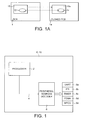
- FIG. 1 shows a typical integrated circuit device (or chip) 10 as known in the art.
- the integrated circuit 10 comprises a plurality of peripheral devices 8 such as those described above, and a processor 2 for executing software.
- the processor 2 is operable, upon executing an instruction to access a peripheral, to output a corresponding peripheral access address onto an address bus 4.
- the address bus 4 connects between the processor 2 and a peripheral address decoder 6.
- the peripheral address decoder 6 is operable to allow the processor 2 to access a peripheral 8 corresponding to the address appearing on the bus 4. In this way, the peripheral address decoder 6 maps access addresses onto respective peripherals 8 of the integrated circuit 10.
- the correlation between the access addresses and their respective peripherals 8 is referred to as the "address map".
- Figure 1A shows a PCB 1 (Printed Circuit Board) on which is mounted an integrated circuit 10 running software 2. If it is possible for an unscrupulous party to obtain information relating to the design of the PCB, then it may be possible to produce a cloned PCB 1 a that functions in a substantially similar manner to the original PCB. If the integrated circuit 10a can be sourced, ostensibly for use with software from another vendor, or in another market, a copy 14 of the required software can be obtained, allowing a fully operational replica of the product to be produced without the authorisation of the software vendor.
- PCB 1 Print Circuit Board
- the present invention seeks to overcome the deficiencies in the prior art by preventing software from running on unauthorised hardware.
- an integrated circuit comprising: a processor; a set of peripherals; a permanent key; transform logic arranged to receive at least one access address from the processor and to transform said at least one access address in dependence on the value of the permanent key to produce a transformed access address; and a peripheral address decoder arranged to receive access addresses including said at least one transformed access address from the processor and to map a respective access address onto each of said peripherals so as to allow the processor to access a corresponding one of said peripherals.
- a method of addressing a peripheral in an integrated circuit comprising a processor and a set of peripherals, the method comprising: receiving an access address from the processor; transforming said access address in dependence on a permanent key incorporated into the integrated circuit to generate a transformed access address; and using the transformed access address to allow the processor to access a corresponding one of said peripherals.
- a method of making an integrated circuit comprising: providing a processor and a set of peripherals; incorporating a permanent key into the integrated circuit; providing a transform logic arranged to receive at least one access address from the processor and to transform said at least one access address in dependence on the value of the permanent key to generate a transformed access address; and providing a peripheral address decoder arranged to receive access addresses including said at least one transformed access address from the processor and to map a respective access address onto each of said peripherals so as to allow the processor to access a corresponding one of said peripherals.
- peripheral address decoder In order for the peripheral address decoder to access a peripheral, software which is produced for the integrated circuit must know the transformed access addresses of the peripherals. That is, it must know the transformed address map, which is a result of a particular value of permanent key. Thus, software produced using an address map corresponding to one particular value of permanent key cannot drive the peripherals of an integrated circuit having a different value of permanent key.
- the permanent key is preferably made inaccessible on the chip, and its value kept secret. Thus the permanent key is difficult to clone.
- the permanent key may comprise a code written to a fuse latch.
- the permanent key may comprise a code held in a ROM (Read Only Memory).
- the permanent key may be of a type that already exists on known chips for another purpose, such as to identify the chip or to enable a particular scrambling or descrambling mode.
- the transform logic may comprise a series of logic gates.
- the logic gates may comprise XOR (exclusive OR) gates.
- the logic gates may each be arranged with one input connected to a respective bit of the permanent key, and one input connected to a respective bit of the address output by the processor.
- the transform logic may comprise a look-up table.
- the above arrangement constitutes a physical barrier to resist the execution of copied software on unauthorised hardware. It is possible to achieve a similar effect by a method of supplying integrated circuits as defined below.
- a method of supplying integrated circuits to first and second users each integrated circuit comprising a processor, a set of peripherals, and an address map for mapping a respective access address onto each of said peripherals; the method comprising: supplying a first integrated circuit having a first address map to the first user, and supplying a second integrated circuit having a second address map to a second user; wherein the first and second integrated circuits are functionally identical except in that the first address map is different from the second address map.
- embodiments of the invention ensure that the IC 10 is made unique to one market, whilst allowing the manufacture of chips (e.g. 10a) that provide an identical set of features for other markets, or for other software/hardware vendors, without the risk that they will be used in cloned PCBs.
- FIG. 2 shows an integrated circuit device (or chip) 10 in accordance with one embodiment of the present invention.
- the integrated circuit 10 comprises a processor 2 for executing software and outputting peripheral access addresses, a plurality of peripherals 8, and peripheral address decoder 6 for receiving peripheral access addresses and allowing the processor to access the corresponding peripherals 8.
- the peripherals 8 include a UART peripheral 8a, a PTI peripheral 8b, a timer 8c, and FDMA peripheral 8d and an MPEG decoder peripheral 8e.
- the processor 2, peripheral address decoder 6, and/or peripherals 8a to 8e may be similar or identical to those described with reference to figure 1.
- the integrated circuit 10 also comprises a permanent key 20 being a value embodied in a permanent storage means of the chip, for example in a fuse latch or ROM included on the chip.
- the integrated circuit 10 further comprises transform logic 18 for transforming peripheral access address received at one input of the transform logic 18 in dependence on a value received at another input of the transform logic 18.
- the processor 2 is connected to the transform logic 18 by processor output address bus 22.
- the permanent key 20 is connected to the transform logic 18 by key bus 24.
- the transform logic is connected to the peripheral address decoder 6 by transformed address bus 26.
- processor output address bus 22 only a particular range of bits on the processor output address bus 22 may be reserved for addressing the peripherals of the chip.
- the second eight bits of a thirty-two bit bus are reserved for the peripherals.
- the remaining bits may be used for other purposes such as addressing external devices or as control bits.
- reference is made to the processor output address or processor output address bus (or similar) it is intended only to refer to those bits that are used to address the peripherals.
- a corresponding access address is output on the processor output address bus 22. This is the address at which the software "sees" the peripheral 8.
- the address on the processor output address bus 22 is received by the transform logic 18 and transformed according to the value of the permanent key 20 that is input via the key bus 24.
- the transformed access address is then output on the transformed address bus 26, and decoded by the peripheral address decoder 6 in order to allow the processor to access the desired peripheral 8.
- the software developer need not know the value of the permanent key 20, but only the corresponding transformed address map.
- the permanent key 20 is preferably made inaccessible and its value is written only shortly before sale. Thus, the value of the key 20 can be kept secret, making it difficult for a useful clone of the chip 10 to be produced.
- the permanent key 20 is written to a fuse latch of the chip.
- the fuse latch comprises a series of fuse elements 28 that are selectively blown in order to permanently program a digital number into the latch.
- This option is particularly advantageous since some integrated circuits may already include a fuse latch for other reasons, such as to identify the chip as being of a particular type (e.g. NDS) or to enable a particular scrambling or descrambling mode used to encode/decode data transmitted on or off chip.
- NDS particular type
- scrambling or descrambling mode used to encode/decode data transmitted on or off chip.
- permanent key it is meant that the key should be impossible, difficult or at least inconvenient to erase or reprogram.
- an eight-bit permanent key 20 is stored in eight one-bit fuse elements 28, one for each bit of the processor output address bus 22.
- the transform logic 18 When a peripheral is to be accessed, the transform logic 18 receives an address output by the processor 2 via the processor output address bus 22. The transform logic 18 is also connected to each fuse element 28 of the permanent key 20 via a respective line of the key bus 24. The transform logic 18 transforms the address input from the processor 2 based on the bits stored in the fuse elements 28 of the permanent key 20, and outputs a transformed peripheral access address on the transformed address bus 26.
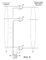
- FIG. 5 shows an exemplary circuit for the transform logic 18, which comprises a set of eight XOR gates 30.
- Each XOR gate 30 has a first input connected to a respective one of the fuse elements 28, the connections between the XOR gates 30 and the fuse elements 28 forming the key bus 24.
- Each XOR gate 30 also has a second input connected to a respective bit of the processor output address bus 22. The outputs of the XOR gates 30 form the transformed address bus 26.
- This arrangement is particularly advantageous since only a small amount of additional circuitry is required on the chip. Further, no extra machine cycles are required for a peripheral access.
- the transform logic comprises a look-up table, whereby an input access address from the processor 2 is referenced against a table of output addresses in dependence on the value of the permanent key 20.
- this option is not preferred since it is generally more expensive and incurs additional machine cycles.
- the transformation is applied to the addresses of all the peripherals. However, it will be appreciated that the transformation could be applied to only some or even one of the addresses. Particularly, unauthorised parties would still be deterred from cloning if the transformed address corresponded to a peripheral 8 that was essential for a wide range of applications, for example the MPEG decoder peripheral.
- the transform logic 18, permanent key 20 and peripheral address decoder 6 are implemented in separate components of the integrated circuit.
- one or both of the transform logic 18 and the permanent key 20 may be incorporated within the peripheral address decoder 6, and/or the transform logic 18 and permanent key 20 may be implemented in the same component.
- Manufacturer A produces an integrated circuit 10 to which is written a particular value of permanent key 20, and provides software developer B with a transformed address map that corresponds to that value.
- the address map may be distributed, for example, in the form of a header file for use when the software is compiled and linked.
- Software developer B is then able to produce software 12 that will correctly drive the peripherals 8 of the integrated circuit 10.
- a third party C attempts to clone the PCB10, then the version of the IC 10a that he is sold will not be written with the correct value of permanent key 20, or perhaps even will not include the transform logic 18 and permanent key 20 at all.
- software 16 copied from developer B will be useless when run on the cloned hardware 14, since the copied software 16 will use a different peripheral address mapping than the cloned chip 14. Therefore a third party is prevented from running copied software on unauthorised hardware.
- the manufacturer A supplies hardware to both parties B and C, but with one address map used in the chips 10 supplied to B and another address map used in the chips 10a supplied to C.
- the chips supplied to both B and C are functionally identical, except in that they use different address maps. In a preferred embodiment, this is achieved by writing one value of permanent key 20a to the chips 10 supplied to B and writing a different value of permanent key 20 to the chips 10 supplied to C. In an alternative embodiment, this is achieved by supplying B with chips that use a different peripheral address decoder 6 (with different a peripheral address map) than the chips supplied to C. In either case, C is prevented from running software copied from B because B's software is produced using an address map that does not match the peripheral mapping of the chips supplied to C. Party C can only run software specifically produced for C's own hardware.
- CLAIMS
Abstract
Description
- The present invention relates to addressing peripherals in integrated circuits, particularly but not exclusively to an integrated circuit having a processor arranged to access a plurality of peripherals, and to methods of making and supplying integrated circuits.
- It is common for an integrated circuit to comprise a processor and a plurality of peripheral devices all incorporated onto the same chip. The processor executes software that controls the behaviour of the processor with respect to the peripherals, and in particular the way in which the peripherals are accessed.
- For example, such integrated circuits may include peripherals such as a UART (Universal Asynchronous Receiver Transmitter) peripheral for transmitting and receiving data asynchronously via the serial port of a computer, a PTI (Programmable Transport Interface) peripheral used to demultiplex DVB standard transport data streams, a timer, an FDMA (Flexible Direct Memory Access) peripheral for moving data from memory to memory, and an MPEG (Moving Picture Experts Group) peripheral for handling digital video functions according to the MPEG standard, decoding frames in a compressed MPEG2 video stream into pictures suitable for display.
- The integrated circuits themselves may be suitable for a wide variety of applications, for example in consumer electronics such as set-top boxes, DVD players, handheld computers and mobile telephones.
- Figure 1 shows a typical integrated circuit device (or chip) 10 as known in the art. The
integrated circuit 10 comprises a plurality ofperipheral devices 8 such as those described above, and aprocessor 2 for executing software. Theprocessor 2 is operable, upon executing an instruction to access a peripheral, to output a corresponding peripheral access address onto anaddress bus 4. Theaddress bus 4 connects between theprocessor 2 and aperipheral address decoder 6. Theperipheral address decoder 6 is operable to allow theprocessor 2 to access a peripheral 8 corresponding to the address appearing on thebus 4. In this way, theperipheral address decoder 6 maps access addresses ontorespective peripherals 8 of theintegrated circuit 10. The correlation between the access addresses and theirrespective peripherals 8 is referred to as the "address map". - However, there is a problem with such devices in that they are susceptible to cloning.
Figure 1A shows a PCB 1 (Printed Circuit Board) on which is mounted an integratedcircuit 10 runningsoftware 2. If it is possible for an unscrupulous party to obtain information relating to the design of the PCB, then it may be possible to produce a clonedPCB 1 a that functions in a substantially similar manner to the original PCB. If the integratedcircuit 10a can be sourced, ostensibly for use with software from another vendor, or in another market, acopy 14 of the required software can be obtained, allowing a fully operational replica of the product to be produced without the authorisation of the software vendor. - It is difficult to physically prevent a PCB from being cloned, but there is a need to provide some kind of obstacle to this cloning process particularly to the extent that it involves copied software on unauthorised hardware.
- The present invention seeks to overcome the deficiencies in the prior art by preventing software from running on unauthorised hardware.
- According to one aspect of the present invention, there is provided an integrated circuit comprising: a processor; a set of peripherals; a permanent key; transform logic arranged to receive at least one access address from the processor and to transform said at least one access address in dependence on the value of the permanent key to produce a transformed access address; and a peripheral address decoder arranged to receive access addresses including said at least one transformed access address from the processor and to map a respective access address onto each of said peripherals so as to allow the processor to access a corresponding one of said peripherals.
- According to another aspect of the present invention, there is provided a method of addressing a peripheral in an integrated circuit comprising a processor and a set of peripherals, the method comprising: receiving an access address from the processor; transforming said access address in dependence on a permanent key incorporated into the integrated circuit to generate a transformed access address; and using the transformed access address to allow the processor to access a corresponding one of said peripherals.
- According to another aspect of the present invention, there is provided a method of making an integrated circuit, the method comprising: providing a processor and a set of peripherals; incorporating a permanent key into the integrated circuit; providing a transform logic arranged to receive at least one access address from the processor and to transform said at least one access address in dependence on the value of the permanent key to generate a transformed access address; and providing a peripheral address decoder arranged to receive access addresses including said at least one transformed access address from the processor and to map a respective access address onto each of said peripherals so as to allow the processor to access a corresponding one of said peripherals.
- In order for the peripheral address decoder to access a peripheral, software which is produced for the integrated circuit must know the transformed access addresses of the peripherals. That is, it must know the transformed address map, which is a result of a particular value of permanent key. Thus, software produced using an address map corresponding to one particular value of permanent key cannot drive the peripherals of an integrated circuit having a different value of permanent key. The permanent key is preferably made inaccessible on the chip, and its value kept secret. Thus the permanent key is difficult to clone.
- The permanent key may comprise a code written to a fuse latch. The permanent key may comprise a code held in a ROM (Read Only Memory).
- The permanent key may be of a type that already exists on known chips for another purpose, such as to identify the chip or to enable a particular scrambling or descrambling mode.
- The transform logic may comprise a series of logic gates. The logic gates may comprise XOR (exclusive OR) gates. The logic gates may each be arranged with one input connected to a respective bit of the permanent key, and one input connected to a respective bit of the address output by the processor.
- Alternatively, the transform logic may comprise a look-up table.
- The above arrangement constitutes a physical barrier to resist the execution of copied software on unauthorised hardware. It is possible to achieve a similar effect by a method of supplying integrated circuits as defined below.
- According to another aspect of the present invention, there is provided a method of supplying integrated circuits to first and second users, each integrated circuit comprising a processor, a set of peripherals, and an address map for mapping a respective access address onto each of said peripherals; the method comprising: supplying a first integrated circuit having a first address map to the first user, and supplying a second integrated circuit having a second address map to a second user; wherein the first and second integrated circuits are functionally identical except in that the first address map is different from the second address map.
- Thus, software produced for the first integrated circuit will not run on the second integrated circuit.
- As described more fully below, embodiments of the invention ensure that the IC 10 is made unique to one market, whilst allowing the manufacture of chips (e.g. 10a) that provide an identical set of features for other markets, or for other software/hardware vendors, without the risk that they will be used in cloned PCBs.
- For a better understanding of the present invention and to show how the same may be carried into effect, reference will now be made, by way of example, to the corresponding drawings in which:
- Figure 1 illustrates an integrated circuit as known in the art;
- Figure 1A illustrates a situation in which copied software is run on cloned hardware;
- Figure 2 illustrates an integrated circuit according to an embodiment of the present invention;
- Figure 3 illustrates a processor output address bus according to an embodiment of the present invention;
- Figure 4 illustrates a permanent key, transform logic and associated connections according an embodiment of the present invention;
- Figure 5 illustrates a more detailed example of Figure 4; and
- Figure 6 illustrates an exemplary application of the present invention.
- Reference is now made to Figure 2, which shows an integrated circuit device (or chip) 10 in accordance with one embodiment of the present invention. The
integrated circuit 10 comprises aprocessor 2 for executing software and outputting peripheral access addresses, a plurality ofperipherals 8, andperipheral address decoder 6 for receiving peripheral access addresses and allowing the processor to access thecorresponding peripherals 8. In this example, theperipherals 8 include a UART peripheral 8a, a PTI peripheral 8b, atimer 8c, and FDMA peripheral 8d and an MPEG decoder peripheral 8e. However, the skilled person will appreciate that other embodiments may comprise any combination of these and/or other peripherals, as appropriate to the application for which the integrated circuit is intended. Theprocessor 2,peripheral address decoder 6, and/orperipherals 8a to 8e may be similar or identical to those described with reference to figure 1. - The integrated
circuit 10 also comprises apermanent key 20 being a value embodied in a permanent storage means of the chip, for example in a fuse latch or ROM included on the chip. Theintegrated circuit 10 further comprisestransform logic 18 for transforming peripheral access address received at one input of thetransform logic 18 in dependence on a value received at another input of thetransform logic 18. - The
processor 2 is connected to thetransform logic 18 by processoroutput address bus 22. Thepermanent key 20 is connected to thetransform logic 18 bykey bus 24. The transform logic is connected to theperipheral address decoder 6 bytransformed address bus 26. - As illustrated in figure 3, only a particular range of bits on the processor
output address bus 22 may be reserved for addressing the peripherals of the chip. In the example shown, the second eight bits of a thirty-two bit bus are reserved for the peripherals. The remaining bits may be used for other purposes such as addressing external devices or as control bits. However, for the purpose of this application, where reference is made to the processor output address or processor output address bus (or similar), it is intended only to refer to those bits that are used to address the peripherals. - In operation, when software running on the
processor 2 instructs the processor to access one of theperipherals 8, a corresponding access address is output on the processoroutput address bus 22. This is the address at which the software "sees" the peripheral 8. The address on the processoroutput address bus 22 is received by thetransform logic 18 and transformed according to the value of thepermanent key 20 that is input via thekey bus 24. The transformed access address is then output on the transformedaddress bus 26, and decoded by theperipheral address decoder 6 in order to allow the processor to access the desired peripheral 8. - Thus, if a software developer is given a transformed address map corresponding to a particular value of
permanent key 20, then the software produced using that mapping will associate a given peripheral with a different address than does theperipheral address decoder 6. The translation between the two addresses is only possible using thecorrect transform logic 18 and value of thepermanent key 20. If thetransform logic 18 is absent, then there will be no translation of the address output by theprocessor 2 and so theperipheral address decoder 6 will not associate this address with the intended peripheral 8. Similarly, if the value of the key 20 is incorrect, the translation will be incorrect and so theperipheral address decoder 6 will not associate the transformed address with the intended peripheral. Thus, software developed for a particular key value will be unable to drive theperipherals 8 of an integrated circuit having a different value. In this way, software can be tied to a particular group of chips, for example to the chips supplied to a particular authorised software developer. - Note that the software developer need not know the value of the
permanent key 20, but only the corresponding transformed address map. Further, thepermanent key 20 is preferably made inaccessible and its value is written only shortly before sale. Thus, the value of the key 20 can be kept secret, making it difficult for a useful clone of thechip 10 to be produced. - In a preferred embodiment, the
permanent key 20 is written to a fuse latch of the chip. The fuse latch comprises a series offuse elements 28 that are selectively blown in order to permanently program a digital number into the latch. This option is particularly advantageous since some integrated circuits may already include a fuse latch for other reasons, such as to identify the chip as being of a particular type (e.g. NDS) or to enable a particular scrambling or descrambling mode used to encode/decode data transmitted on or off chip. Thus, by using or extending an existing fuse latch, it is possible to minimise the amount of additional circuitry required on thechip 10. - However, it should be appreciated that other means for storing the
permanent key 20 could be used, such as a ROM. Note that by "permanent key" it is meant that the key should be impossible, difficult or at least inconvenient to erase or reprogram. - A preferred embodiment is now described with reference to figures 4 and 5. As shown in figure 4, an eight-bit
permanent key 20 is stored in eight one-bit fuse elements 28, one for each bit of the processoroutput address bus 22. - When a peripheral is to be accessed, the
transform logic 18 receives an address output by theprocessor 2 via the processoroutput address bus 22. Thetransform logic 18 is also connected to eachfuse element 28 of thepermanent key 20 via a respective line of thekey bus 24. Thetransform logic 18 transforms the address input from theprocessor 2 based on the bits stored in thefuse elements 28 of thepermanent key 20, and outputs a transformed peripheral access address on the transformedaddress bus 26. - Figure 5 shows an exemplary circuit for the
transform logic 18, which comprises a set of eightXOR gates 30. EachXOR gate 30 has a first input connected to a respective one of thefuse elements 28, the connections between theXOR gates 30 and thefuse elements 28 forming thekey bus 24. EachXOR gate 30 also has a second input connected to a respective bit of the processoroutput address bus 22. The outputs of theXOR gates 30 form the transformedaddress bus 26. - Thus, if a given
fuse element 28 is set at logic-0, the correspondingXOR gate 30 will be transparent and the bit output by that gate will be equal to the bit input from theprocessor 2. On the other hand, if the fuse element is set at logic-1, the bit output by the correspondingXOR gate 30 will be the complement of the bit input from theprocessor 2. In this way, the processor output address will be transformed in dependence on the value of thepermanent key 20. Other gate arrangements will be apparent to a person skilled in the art. - This arrangement is particularly advantageous since only a small amount of additional circuitry is required on the chip. Further, no extra machine cycles are required for a peripheral access.
- In an alternative embodiment, the transform logic comprises a look-up table, whereby an input access address from the
processor 2 is referenced against a table of output addresses in dependence on the value of thepermanent key 20. However, this option is not preferred since it is generally more expensive and incurs additional machine cycles. - In preferred embodiments, the transformation is applied to the addresses of all the peripherals. However, it will be appreciated that the transformation could be applied to only some or even one of the addresses. Particularly, unauthorised parties would still be deterred from cloning if the transformed address corresponded to a peripheral 8 that was essential for a wide range of applications, for example the MPEG decoder peripheral.
- In one embodiment, the
transform logic 18,permanent key 20 andperipheral address decoder 6 are implemented in separate components of the integrated circuit. However, in alternative embodiments, one or both of thetransform logic 18 and thepermanent key 20 may be incorporated within theperipheral address decoder 6, and/or thetransform logic 18 and permanent key 20 may be implemented in the same component. - An application of the present invention is now described with reference to figure 6. Manufacturer A produces an
integrated circuit 10 to which is written a particular value ofpermanent key 20, and provides software developer B with a transformed address map that corresponds to that value. The address map may be distributed, for example, in the form of a header file for use when the software is compiled and linked. Software developer B is then able to producesoftware 12 that will correctly drive theperipherals 8 of theintegrated circuit 10. However, if a third party C attempts to clone the PCB10, then the version of theIC 10a that he is sold will not be written with the correct value ofpermanent key 20, or perhaps even will not include thetransform logic 18 and permanent key 20 at all. As a result, software 16 copied from developer B will be useless when run on the clonedhardware 14, since the copied software 16 will use a different peripheral address mapping than the clonedchip 14. Therefore a third party is prevented from running copied software on unauthorised hardware. - In another application, the manufacturer A supplies hardware to both parties B and C, but with one address map used in the
chips 10 supplied to B and another address map used in thechips 10a supplied to C. The chips supplied to both B and C are functionally identical, except in that they use different address maps. In a preferred embodiment, this is achieved by writing one value of permanent key 20a to thechips 10 supplied to B and writing a different value of permanent key 20 to thechips 10 supplied to C. In an alternative embodiment, this is achieved by supplying B with chips that use a different peripheral address decoder 6 (with different a peripheral address map) than the chips supplied to C. In either case, C is prevented from running software copied from B because B's software is produced using an address map that does not match the peripheral mapping of the chips supplied to C. Party C can only run software specifically produced for C's own hardware.CLAIMS:
Claims (29)
- An integrated circuit (10) comprising:a processor (2);a set of peripherals (8);a permanent key (20);transform logic (18) arranged to receive at least one access address from the processor (2) and to transform said at least one access address in dependence on the value of the permanent key (20) to produce a transformed access address; anda peripheral address decoder (6) arranged to receive access addresses including said at least one transformed access address from the processor (2) and to map a respective access address onto each of said peripherals (8) so as to allow the processor (2) to access a corresponding one of said peripherals (8).
- An integrated circuit according to claim 1, wherein the permanent key (20) is written to a fuse latch of the integrated circuit (10).
- An integrated circuit according to claim 1, wherein the permanent key (20) is held within a ROM of the integrated circuit (10).
- An integrated circuit according to any preceding claim, wherein at least part of the permanent key (20) is arranged to provide another chip-related function in addition to its function in transforming an access address of a peripheral (8).
- An integrated circuit according to claim 4, wherein the permanent key (20) provides at least one of the functions of: identifying the integrated circuit (10), enabling a scrambling mode, and enabling a descrambling mode.
- An integrated circuit according to any preceding claim, wherein the transform logic (18) comprises a set of logic gates.
- An integrated circuit according to claim 6, wherein the set of logic gates comprises a set of XOR gates (30).
- An integrated circuit according to claim 6 or 7, wherein the permanent key (20) comprises a plurality of bits, and the logic gates are each arranged with one input connected to a respective bit of the permanent key (20) and one input connected to a respective bit of the address output by the processor (2).
- An integrated circuit according to any of claims 1 to 5, wherein the transform logic (18) comprises a look-up table.
- An integrated circuit according to any preceding claim, wherein at least one of the peripherals (8) comprises one of the following: a UART peripheral (8a), a PTI peripheral (8b), a timer (8c), an FDMA peripheral (8d), and an MPEG decoder peripheral (8e).
- An integrated circuit according to any preceding claim, wherein the integrated circuit (10) is suitable for use in at least one of: a set-top box, a DVD player, a handheld computer and a mobile telephone.
- An integrated circuit according to any preceding claim, wherein the peripheral address decoder (6), transform logic (18) and permanent key (20) are each implemented on separate components on the integrated circuit (10).
- An integrated circuit according to any of claims 1 to 11, wherein at least two of the peripheral address decoder (6), transform logic (19) and permanent key (20) are incorporated into the same component of the integrated circuit (20).
- A method of addressing a peripheral (8) in an integrated circuit (10) comprising a processor (2) and a set of peripherals (8), the method comprising:receiving an access address from the processor (2);transforming said access address in dependence on a permanent key (20) incorporated into the integrated circuit (10) to generate a transformed access address; andusing the transformed access address to allow the processor (2) to access a corresponding one of said peripherals (8).
- A method according to claim 14, and the step of transforming said access address comprises reading the value of the permanent key (20) from a fuse latch.
- A method according to claim 14, wherein the step of transforming said access address comprises reading the value of the permanent key (20) from a ROM.
- A method according to any of claims 14 to 16, further comprising a step of using the permanent key (20) to provide another chip-related function in addition to the step of transforming an access address of a peripheral (8).
- A method according to claim 17, wherein providing another chip-related function comprises providing at least one of the functions of: identifying the integrated circuit (10), enabling a scrambling mode, and enabling a descrambling mode
- A method according to any of claims 14 to 18, wherein the permanent key (20) comprises a plurality of bits, and the step of transforming said access address comprises performing a logic operation on each bit of said access address in conjunction with a respective bit of the permanent key (20).
- A method according to claim 19, wherein said logic operation comprises taking the exclusive-OR of said bit of said access address and the respective bit of the permanent key (20).
- A method of making an integrated circuit, the method comprising:providing a processor (2) and a set of peripherals (8),incorporating a permanent key (20) into the integrated circuit (10);providing a transform logic (18) to receive at least one access address from the processor (2) and to transform said at least one access address in dependence on the value of the permanent key (20) to generate a transformed access address; andproviding a peripheral address decoder (6) arranged to receive access addresses including said at least one transformed access address from the processor (2) and to map a respective access address onto each of said peripherals (8) so as to allow the processor (2) to access a corresponding one of said peripherals (8).
- A method of supplying integrated circuits to first and second users, each integrated circuit comprising a processor, a set of peripherals, and an address map for mapping a respective access address onto each of said peripherals; the method comprising:supplying a first integrated circuit having a first address map to the first user, and supplying a second integrated circuit having a second address map to a second user; wherein the first and second integrated circuits are functionally identical except in that the first address map is different from the second address map.
- A method according to claim 22, wherein the first map is the result of a first transformation applied to at least one peripheral access address output by a processor of the first integrated circuit, and the second address map is the result of a second transformation applied to at least one peripheral access address output by a processor of the second integrated circuit.
- A method according to claim 23, wherein the first transformation is performed based on the value of a first permanent key incorporated into the first integrated circuit, and the second transformation is performed based on the value of a second permanent key incorporated into the second integrated circuit.
- A method according to claim 22, wherein the first address map is a property of a first peripheral address decoder of the first integrated circuit, and the second address map is a property of a second peripheral address decoder of the second integrated circuit.
- A set-top box having an integrated circuit comprising:a processor;a set of peripherals;a permanent key;transform logic arranged to receive at least one access address from the processor and to transform said at least one access address in dependence on the value of the permanent key to produce a transformed access address; anda peripheral address decoder arranged to receive access addresses including said at least one transformed access address from the processor and to map a respective access address onto each of said peripherals so as to allow the processor to access a corresponding one of said peripherals.
- A DVD player having an integrated circuit comprising:a processor;a set of peripherals;a permanent key;transform logic arranged to receive at least one access address from the processor and to transform said at least one access address in dependence on the value of the permanent key to produce a transformed access address; anda peripheral address decoder arranged to receive access addresses including said at least one transformed access address from the processor and to map a respective access address onto each of said peripherals so as to allow the processor to access a corresponding one of said peripherals.
- A mobile telephone having an integrated circuit comprising:a processor;a set of peripherals;a permanent key;transform logic arranged to receive at least one access address from the processor and to transform said at least one access address in dependence on the value of the permanent key to produce a transformed access address; anda peripheral address decoder arranged to receive access addresses including said at least one transformed access address from the processor and to map a respective access address onto each of said peripherals so as to allow the processor to access a corresponding one of said peripherals.
- A handheld computer having an integrated circuit comprising:a processor;a set of peripherals;a permanent key;transform logic arranged to receive at least one access address from the processor and to transform said at least one access address in dependence on the value of the permanent key to produce a transformed access address; anda peripheral address decoder arranged to receive access addresses including said at least one transformed access address from the processor and to map a respective access address onto each of said peripherals so as to allow the processor to access a corresponding one of said peripherals.
Priority Applications (2)
| Application Number | Priority Date | Filing Date | Title |
|---|---|---|---|
| EP05255900A EP1768028A1 (en) | 2005-09-22 | 2005-09-22 | Addressing peripherals in an ic |
| US11/525,253 US8151120B2 (en) | 2005-09-22 | 2006-09-21 | Addressing peripherals in an IC |
Applications Claiming Priority (1)
| Application Number | Priority Date | Filing Date | Title |
|---|---|---|---|
| EP05255900A EP1768028A1 (en) | 2005-09-22 | 2005-09-22 | Addressing peripherals in an ic |
Publications (1)
| Publication Number | Publication Date |
|---|---|
| EP1768028A1 true EP1768028A1 (en) | 2007-03-28 |
Family
ID=35482827
Family Applications (1)
| Application Number | Title | Priority Date | Filing Date |
|---|---|---|---|
| EP05255900A Withdrawn EP1768028A1 (en) | 2005-09-22 | 2005-09-22 | Addressing peripherals in an ic |
Country Status (2)
| Country | Link |
|---|---|
| US (1) | US8151120B2 (en) |
| EP (1) | EP1768028A1 (en) |
Citations (5)
| Publication number | Priority date | Publication date | Assignee | Title |
|---|---|---|---|---|
| US4278837A (en) * | 1977-10-31 | 1981-07-14 | Best Robert M | Crypto microprocessor for executing enciphered programs |
| US20030188178A1 (en) * | 2002-03-27 | 2003-10-02 | Strongin Geoffrey S. | System and method providing region-granular, hardware-controlled memory encryption |
| WO2004046935A2 (en) * | 2002-11-21 | 2004-06-03 | Philips Intellectual Property & Standards Gmbh | Circuit arrangement with non-volatile memory module and method of en-/decrypting data in the non-volatile memory module |
| US20040128458A1 (en) * | 2001-05-17 | 2004-07-01 | Wolfgang Buhr | Method and device for protecting data transmission between a central processor and a memory |
| FR2857804A1 (en) | 2003-07-17 | 2005-01-21 | Atmel Corp | System for smoothing the current consumption in a digital logical module, e.g. a chip card, comprises a smoothing circuit that outputs a signal when a processing circuit is inactive |
Family Cites Families (7)
| Publication number | Priority date | Publication date | Assignee | Title |
|---|---|---|---|---|
| GB2276254B (en) * | 1993-03-20 | 1997-10-01 | Motorola Inc | Data storage device |
| US5892826A (en) * | 1996-01-30 | 1999-04-06 | Motorola, Inc. | Data processor with flexible data encryption |
| FR2804525A1 (en) * | 2000-01-27 | 2001-08-03 | St Microelectronics Sa | SYSTEM FOR MANAGING PERIPHERALS IN AN INTEGRATED CIRCUIT |
| JP2002041495A (en) * | 2000-07-21 | 2002-02-08 | Denso Corp | Microcomputer |
| FR2825873A1 (en) * | 2001-06-11 | 2002-12-13 | St Microelectronics Sa | PROTECTED STORAGE OF DATA IN AN INTEGRATED CIRCUIT |
| US20040225881A1 (en) * | 2002-12-02 | 2004-11-11 | Walmsley Simon Robert | Variant keys |
| US7263623B1 (en) * | 2004-03-30 | 2007-08-28 | Altera Corporation | Microprocessor system |
-
2005
- 2005-09-22 EP EP05255900A patent/EP1768028A1/en not_active Withdrawn
-
2006
- 2006-09-21 US US11/525,253 patent/US8151120B2/en active Active
Patent Citations (5)
| Publication number | Priority date | Publication date | Assignee | Title |
|---|---|---|---|---|
| US4278837A (en) * | 1977-10-31 | 1981-07-14 | Best Robert M | Crypto microprocessor for executing enciphered programs |
| US20040128458A1 (en) * | 2001-05-17 | 2004-07-01 | Wolfgang Buhr | Method and device for protecting data transmission between a central processor and a memory |
| US20030188178A1 (en) * | 2002-03-27 | 2003-10-02 | Strongin Geoffrey S. | System and method providing region-granular, hardware-controlled memory encryption |
| WO2004046935A2 (en) * | 2002-11-21 | 2004-06-03 | Philips Intellectual Property & Standards Gmbh | Circuit arrangement with non-volatile memory module and method of en-/decrypting data in the non-volatile memory module |
| FR2857804A1 (en) | 2003-07-17 | 2005-01-21 | Atmel Corp | System for smoothing the current consumption in a digital logical module, e.g. a chip card, comprises a smoothing circuit that outputs a signal when a processing circuit is inactive |
Also Published As
| Publication number | Publication date |
|---|---|
| US20070106820A1 (en) | 2007-05-10 |
| US8151120B2 (en) | 2012-04-03 |
Similar Documents
| Publication | Publication Date | Title |
|---|---|---|
| KR100974973B1 (en) | Accessing private data about the state of a data processing machine from storage that is publicly accessible | |
| CN107004070B (en) | Media decoding control with hardware protected digital rights management | |
| US8533856B2 (en) | Secure compact flash | |
| CN101454783B (en) | Systems and methods for datapath security in a system-on-a-chip device | |
| EP2161671A2 (en) | Device with privileged memory and applications thereof | |
| US20080092210A1 (en) | Electronic apparatus and firmware protection method | |
| US20030221066A1 (en) | Memory card and memory card data recording method | |
| US20070162964A1 (en) | Embedded system insuring security and integrity, and method of increasing security thereof | |
| EP1845470A1 (en) | Multiple purpose integrated circuit | |
| US8166561B2 (en) | Security device, secure memory system and method using a security device | |
| JPS59139200A (en) | Protector for solid memory | |
| BRPI9813309B1 (en) | method for downloading an executable application into a decoder and said decoder | |
| FI110294B (en) | Smart card messaging without microprocessor intervention | |
| JPH10133762A (en) | Computer equipped with software selecting function | |
| JP2004013905A (en) | Use of hashing in secure bootloader | |
| WO1998016887A1 (en) | Method of switching video source transferred by using zv port, and computer system using the method | |
| CN103282913B (en) | For loading the method for the code of at least one software module | |
| CN101627364A (en) | Data structure for identifying hardware and software licenses to distribute with a complying device | |
| US8745410B2 (en) | Method and apparatus to scramble data stored in memories accessed by microprocessors | |
| US5928362A (en) | Peripheral card security and configuration interface | |
| US20020156712A1 (en) | Parametric representation scheme and systems for description and reconstruction of an intellectual property management and protection system and corresponding protected media | |
| KR101311963B1 (en) | Semiconductor memory device capable of writing and reading safely from power attack and method thereof | |
| US7313096B2 (en) | Multiplexing a communication port | |
| US20080172336A1 (en) | Content Distribution | |
| JP2005209108A (en) | Microcomputer with external memory |
Legal Events
| Date | Code | Title | Description |
|---|---|---|---|
| PUAI | Public reference made under article 153(3) epc to a published international application that has entered the european phase |
Free format text: ORIGINAL CODE: 0009012 |
|
| AK | Designated contracting states |
Kind code of ref document: A1 Designated state(s): AT BE BG CH CY CZ DE DK EE ES FI FR GB GR HU IE IS IT LI LT LU LV MC NL PL PT RO SE SI SK TR |
|
| AX | Request for extension of the european patent |
Extension state: AL BA HR MK YU |
|
| 17P | Request for examination filed |
Effective date: 20070918 |
|
| 17Q | First examination report despatched |
Effective date: 20071022 |
|
| AKX | Designation fees paid |
Designated state(s): DE FR GB IT |
|
| STAA | Information on the status of an ep patent application or granted ep patent |
Free format text: STATUS: THE APPLICATION IS DEEMED TO BE WITHDRAWN |
|
| 18D | Application deemed to be withdrawn |
Effective date: 20081024 |