EP1130909A2 - Field synchronization system maintaining interlace integrity - Google Patents
Field synchronization system maintaining interlace integrity Download PDFInfo
- Publication number
- EP1130909A2 EP1130909A2 EP01111808A EP01111808A EP1130909A2 EP 1130909 A2 EP1130909 A2 EP 1130909A2 EP 01111808 A EP01111808 A EP 01111808A EP 01111808 A EP01111808 A EP 01111808A EP 1130909 A2 EP1130909 A2 EP 1130909A2
- Authority
- EP
- European Patent Office
- Prior art keywords
- video
- signal
- picture
- field type
- field
- Prior art date
- Legal status (The legal status is an assumption and is not a legal conclusion. Google has not performed a legal analysis and makes no representation as to the accuracy of the status listed.)
- Ceased
Links
- 238000000034 method Methods 0.000 claims description 16
- 230000015654 memory Effects 0.000 abstract description 43
- 230000001360 synchronised effect Effects 0.000 abstract description 18
- 230000001934 delay Effects 0.000 abstract description 4
- 238000012937 correction Methods 0.000 abstract description 3
- 238000010586 diagram Methods 0.000 description 21
- 238000007906 compression Methods 0.000 description 18
- 230000006835 compression Effects 0.000 description 18
- 238000012545 processing Methods 0.000 description 16
- 239000002131 composite material Substances 0.000 description 10
- 230000006870 function Effects 0.000 description 10
- 230000009467 reduction Effects 0.000 description 8
- 230000000630 rising effect Effects 0.000 description 6
- 230000003044 adaptive effect Effects 0.000 description 5
- 239000003990 capacitor Substances 0.000 description 5
- 230000003111 delayed effect Effects 0.000 description 5
- 230000000694 effects Effects 0.000 description 5
- 238000005070 sampling Methods 0.000 description 5
- 230000008859 change Effects 0.000 description 4
- 230000033001 locomotion Effects 0.000 description 4
- 230000008569 process Effects 0.000 description 4
- 230000009471 action Effects 0.000 description 3
- 238000012360 testing method Methods 0.000 description 3
- 238000006243 chemical reaction Methods 0.000 description 2
- 238000013144 data compression Methods 0.000 description 2
- 230000002708 enhancing effect Effects 0.000 description 2
- 238000013139 quantization Methods 0.000 description 2
- 101710148588 ADP,ATP carrier protein 2 Proteins 0.000 description 1
- 101710165307 ADP,ATP carrier protein 2, mitochondrial Proteins 0.000 description 1
- 102100032533 ADP/ATP translocase 1 Human genes 0.000 description 1
- 102100026396 ADP/ATP translocase 2 Human genes 0.000 description 1
- 101710102718 ADP/ATP translocase 2 Proteins 0.000 description 1
- 101710102715 ADP/ATP translocase 3 Proteins 0.000 description 1
- 101150093547 AUX1 gene Proteins 0.000 description 1
- 101000768061 Escherichia phage P1 Antirepressor protein 1 Proteins 0.000 description 1
- 108010014173 Factor X Proteins 0.000 description 1
- 101000796932 Homo sapiens ADP/ATP translocase 1 Proteins 0.000 description 1
- 101100367246 Saccharomyces cerevisiae (strain ATCC 204508 / S288c) SWA2 gene Proteins 0.000 description 1
- 230000005540 biological transmission Effects 0.000 description 1
- 239000000919 ceramic Substances 0.000 description 1
- 230000001010 compromised effect Effects 0.000 description 1
- 230000007423 decrease Effects 0.000 description 1
- 238000013461 design Methods 0.000 description 1
- 230000009977 dual effect Effects 0.000 description 1
- 230000001747 exhibiting effect Effects 0.000 description 1
- 244000145841 kine Species 0.000 description 1
- 238000007726 management method Methods 0.000 description 1
- 239000003550 marker Substances 0.000 description 1
- 239000000463 material Substances 0.000 description 1
- 239000000203 mixture Substances 0.000 description 1
- 238000012986 modification Methods 0.000 description 1
- 230000004048 modification Effects 0.000 description 1
- 230000000750 progressive effect Effects 0.000 description 1
- 230000002441 reversible effect Effects 0.000 description 1
- 230000008054 signal transmission Effects 0.000 description 1
- 230000005236 sound signal Effects 0.000 description 1
- 238000012549 training Methods 0.000 description 1
Images


Classifications
-
- H—ELECTRICITY
- H04—ELECTRIC COMMUNICATION TECHNIQUE
- H04N—PICTORIAL COMMUNICATION, e.g. TELEVISION
- H04N9/00—Details of colour television systems
- H04N9/64—Circuits for processing colour signals
- H04N9/641—Multi-purpose receivers, e.g. for auxiliary information
-
- G06T3/04—
-
- G—PHYSICS
- G06—COMPUTING; CALCULATING OR COUNTING
- G06T—IMAGE DATA PROCESSING OR GENERATION, IN GENERAL
- G06T3/00—Geometric image transformation in the plane of the image
- G06T3/40—Scaling the whole image or part thereof
- G06T3/4007—Interpolation-based scaling, e.g. bilinear interpolation
-
- H—ELECTRICITY
- H04—ELECTRIC COMMUNICATION TECHNIQUE
- H04N—PICTORIAL COMMUNICATION, e.g. TELEVISION
- H04N19/00—Methods or arrangements for coding, decoding, compressing or decompressing digital video signals
- H04N19/90—Methods or arrangements for coding, decoding, compressing or decompressing digital video signals using coding techniques not provided for in groups H04N19/10-H04N19/85, e.g. fractals
-
- H—ELECTRICITY
- H04—ELECTRIC COMMUNICATION TECHNIQUE
- H04N—PICTORIAL COMMUNICATION, e.g. TELEVISION
- H04N3/00—Scanning details of television systems; Combination thereof with generation of supply voltages
- H04N3/10—Scanning details of television systems; Combination thereof with generation of supply voltages by means not exclusively optical-mechanical
- H04N3/16—Scanning details of television systems; Combination thereof with generation of supply voltages by means not exclusively optical-mechanical by deflecting electron beam in cathode-ray tube, e.g. scanning corrections
- H04N3/22—Circuits for controlling dimensions, shape or centering of picture on screen
- H04N3/223—Controlling dimensions
-
- H—ELECTRICITY
- H04—ELECTRIC COMMUNICATION TECHNIQUE
- H04N—PICTORIAL COMMUNICATION, e.g. TELEVISION
- H04N3/00—Scanning details of television systems; Combination thereof with generation of supply voltages
- H04N3/10—Scanning details of television systems; Combination thereof with generation of supply voltages by means not exclusively optical-mechanical
- H04N3/16—Scanning details of television systems; Combination thereof with generation of supply voltages by means not exclusively optical-mechanical by deflecting electron beam in cathode-ray tube, e.g. scanning corrections
- H04N3/22—Circuits for controlling dimensions, shape or centering of picture on screen
- H04N3/227—Centering
-
- H—ELECTRICITY
- H04—ELECTRIC COMMUNICATION TECHNIQUE
- H04N—PICTORIAL COMMUNICATION, e.g. TELEVISION
- H04N3/00—Scanning details of television systems; Combination thereof with generation of supply voltages
- H04N3/10—Scanning details of television systems; Combination thereof with generation of supply voltages by means not exclusively optical-mechanical
- H04N3/16—Scanning details of television systems; Combination thereof with generation of supply voltages by means not exclusively optical-mechanical by deflecting electron beam in cathode-ray tube, e.g. scanning corrections
- H04N3/27—Circuits special to multi-standard receivers
-
- H—ELECTRICITY
- H04—ELECTRIC COMMUNICATION TECHNIQUE
- H04N—PICTORIAL COMMUNICATION, e.g. TELEVISION
- H04N5/00—Details of television systems
- H04N5/222—Studio circuitry; Studio devices; Studio equipment
- H04N5/262—Studio circuits, e.g. for mixing, switching-over, change of character of image, other special effects ; Cameras specially adapted for the electronic generation of special effects
- H04N5/2624—Studio circuits, e.g. for mixing, switching-over, change of character of image, other special effects ; Cameras specially adapted for the electronic generation of special effects for obtaining an image which is composed of whole input images, e.g. splitscreen
-
- H—ELECTRICITY
- H04—ELECTRIC COMMUNICATION TECHNIQUE
- H04N—PICTORIAL COMMUNICATION, e.g. TELEVISION
- H04N5/00—Details of television systems
- H04N5/44—Receiver circuitry for the reception of television signals according to analogue transmission standards
- H04N5/445—Receiver circuitry for the reception of television signals according to analogue transmission standards for displaying additional information
- H04N5/45—Picture in picture, e.g. displaying simultaneously another television channel in a region of the screen
-
- H—ELECTRICITY
- H04—ELECTRIC COMMUNICATION TECHNIQUE
- H04N—PICTORIAL COMMUNICATION, e.g. TELEVISION
- H04N7/00—Television systems
- H04N7/007—Systems with supplementary picture signal insertion during a portion of the active part of a television signal, e.g. during top and bottom lines in a HDTV letter-box system
-
- H—ELECTRICITY
- H04—ELECTRIC COMMUNICATION TECHNIQUE
- H04N—PICTORIAL COMMUNICATION, e.g. TELEVISION
- H04N7/00—Television systems
- H04N7/01—Conversion of standards, e.g. involving analogue television standards or digital television standards processed at pixel level
-
- H—ELECTRICITY
- H04—ELECTRIC COMMUNICATION TECHNIQUE
- H04N—PICTORIAL COMMUNICATION, e.g. TELEVISION
- H04N7/00—Television systems
- H04N7/01—Conversion of standards, e.g. involving analogue television standards or digital television standards processed at pixel level
- H04N7/0105—Conversion of standards, e.g. involving analogue television standards or digital television standards processed at pixel level using a storage device with different write and read speed
-
- H—ELECTRICITY
- H04—ELECTRIC COMMUNICATION TECHNIQUE
- H04N—PICTORIAL COMMUNICATION, e.g. TELEVISION
- H04N7/00—Television systems
- H04N7/01—Conversion of standards, e.g. involving analogue television standards or digital television standards processed at pixel level
- H04N7/0117—Conversion of standards, e.g. involving analogue television standards or digital television standards processed at pixel level involving conversion of the spatial resolution of the incoming video signal
- H04N7/0122—Conversion of standards, e.g. involving analogue television standards or digital television standards processed at pixel level involving conversion of the spatial resolution of the incoming video signal the input and the output signals having different aspect ratios
-
- H—ELECTRICITY
- H04—ELECTRIC COMMUNICATION TECHNIQUE
- H04N—PICTORIAL COMMUNICATION, e.g. TELEVISION
- H04N7/00—Television systems
- H04N7/015—High-definition television systems
-
- H—ELECTRICITY
- H04—ELECTRIC COMMUNICATION TECHNIQUE
- H04N—PICTORIAL COMMUNICATION, e.g. TELEVISION
- H04N9/00—Details of colour television systems
- H04N9/64—Circuits for processing colour signals
Definitions
- the invention relates to the field of televisions having multiple picture displays for asynchronous video signals, and in particular, to such televisions having a wide display format ratio screen.
- Most televisions today have a format display ratio, horizontal width to vertical height, of 4:3.
- a wide format display ratio corresponds more closely to the display format ratio of movies, for example 16:9.
- the invention is applicable to both direct view televisions and projection televisions.
- Televisions having a format display ratio of 4:3, often referred to as 4 X 3, are limited in the ways that single and multiple video signal sources can be displayed.
- Television signal transmissions of commercial broadcasters, except for experimental material, are broadcast with a 4 X 3 format display ratio.
- Many viewers find the 4 X 3 display format less pleasing than the wider format display ratio associated with the movies.
- Televisions with a wide format display ratio provide not only a more pleasing display, but are capable of displaying wide display format signal sources in a corresponding wide display format. Movies "look" like movies, not cropped or distorted versions thereof.
- the video source need not be cropped, either when converted from film to video, for example with a telecine device, or by processors in the television.
- a wide screen television according to the various aspects of this invention is capable of providing high resolution, single and multiple picture displays, from single and multiple asynchronous sources having similar or different format ratios, and with selectable display format ratios.
- auxiliary picture When an auxiliary picture is a small inset, various artifacts from imprecise synchronization with the main signal are tolerable. However, for some formats particularly suited for a wide screen television, such as two side by side pictures of equal size, such imprecision and artifacts cannot be tolerated. The large size of the auxiliary picture can make such artifacts painfully obvious.
- the video display and deflection system for composite picture displays is synchronized with the main video signal.
- the auxiliary video signal must be vertically synchronized with the main video signal and the video display.
- the auxiliary video signal can be delayed by a fraction of a field period in a field memory, and then speeded up in a line memory.
- a four field synchronization system utilizes four dual port asynchronous field memories.
- Asynchronous memories that is, those having independent write and read clock ports, are generally more expensive than synchronous memories.
- a degree of field synchronization can be achieved which substantially matches the performance of a four field system, but utilizes only a single synchronous video RAM as a field memory and a single asynchronous first in first out (FIFO) multiple line memory device.
- FIFO first in first out
- the following artifacts can be encountered: (1) Two frame line shifts and 1 field line shift will occur each time the two signals precess through a video frame; and, (2) The auxiliary channel video gets scrambled at the bottom of the picture whenever the precession rate between the main and auxiliary signals if greater than two lines per frame. This precession rate has been found not likely to occur in the consumer electronics environment.
- the cost saving over a four field system is approximately 4:1, without incurring any significant sacrifice in performance.
- the size of the FIFO is related to the minimum line storage capacity thought to be reasonably necessary to avoid read/write pointer collisions. Read/write pointer collisions occur when old data is read out of the FIFO before new data has an opportunity to be written into the FIFO. Read/write pointer collisions also occur when new data overwrites the memory before the old data has an opportunity to be read out of the FIFO.
- the size of FIFO utilized herein, for example 2048 X 8, corresponds to approximately five lines.
- a field synchronization system for asynchronous video signals comprises a video display synchronized with a first video signal.
- the first video signal has a first line rate component and a first field rate component, corresponding to the horizontal and vertical synchronizing components of the first video signal.
- a field memory having synchronous write and read ports, is provided for a second video signal.
- the second video signal has a second line rate component, corresponding to the horizontal synchronizing component of the second video signal.
- a multiple line memory (FIFO) for the second video signal has asynchronous write and read ports and independently resettable write and read pointers. The second video signal, subsampled if necessary, is stored in the field memory and written to the field memory synchronously with the second line rate component.
- the second video signal, subsampled if necessary, is written into the multiple line memory synchronously with the second line rate component.
- the data corresponding to the second video signal is therefor completely orthogonal, having been subsampled and stored synchronously with its own synchronizing components.
- the second video signal, subsampled if necessary, is read from the multiple line memory synchronously with the first line rate component.
- a sampling and delay circuit controls resetting the write and read pointers.
- a write pointer reset signal is generated by sampling the first field rate component with the second line rate component.
- the write pointer is reset up to one line period of the second video signal after every start of field of the first video signal.
- a read pointer reset signal is generated by sampling the first field rate component with the first line rate component.
- the read pointer is reset at least two line periods of the first video signal after every start of field of the first video signal, and more particularly, at least two but not more than three line periods of the first video signal after every start of field of the first video signal.
- Data blocks from the video RAM are written into 2048 x 8 FIFO with the same clock was used to sample the video data, for example a 640f H clock which is locked to the auxiliary signal, rather than the main signal.
- the FIFO is read using the display clock frequency, for example 1024f H , which is locked to horizontal synchronizing component of the main video channel.
- the use of a multiple line memory (FIFO) which has independent read and write port clocks enables data which was orthogonally sampled at a first rate to be displayed orthogonally at a second rate.
- the use of the asynchronous FIFO for the auxiliary channel does not solve all of the problems associated with video synchronization.
- Maintaining interlace integrity of the auxiliary channel video is a problem stemming from reading and writing of the FIFO in the auxiliary signal path asynchronously relative to the main signal. Since the display is locked to the main channel video, the current field type being displayed, that is the upper or lower field, will be determined by the main signal.
- the field type which is stored in a video RAM memory in the auxiliary signal path or channel for synchronization with the main signal, and ready to be read out at the start of the main channel field, may or may not be the same as the displayed field type. It may be necessary to change the auxiliary signal field type stored in the video RAM to match that of the main channel display.
- a digitizing process for an NTSC signal will quantize 262.5 line fields of the NTSC signal into 263 line upper fields (U, sometimes referred to odd fields) and 262 line lower, fields (L, sometimes called even fields). This is due to fact that vertical sync is sampled with pulses representing horizontal sync.
- the upper fields include odd lines 1 through 263.
- the lower fields include even lines 2 through 262.
- a first field type indicator U/L(A) represents the field type stored in the auxiliary channel video RAM if each auxiliary channel line were written in "normally". The term normal is used here to indicate that the odd lines 1-263 are written in to the video RAM as the upper field is being received and decoded.
- a second field type indicator U/L(B) represents the field type stored in the video RAM if the first line of the upper field is not written into the video RAM during the reception of an upper field. Instead, the first line is actually tacked onto the last line (number 262) of the lower field.
- a third field type indicator U/L(C) represents the field type stored in the video RAM if the last line of the upper field is added to the video RAM during the reception of the lower field. This effectively inverts the field type, since line 263 will be the first displayed line and line 1 will be the second displayed line.
- the addition and subtraction of lines in modes B and C does not degrade the auxiliary channel picture because these lines occur during vertical retrace or overscan.
- a synchronization system for asynchronous video signals comprises first and second field type detectors for first and second video signals respectively, each having an output indicating whether the respective video signal has a first or second field type.
- a video memory for example a synchronous video RAM and an asynchronous multiple line FIFO, synchronize the second video signal with the first video signal for a combined display.
- a field reversing circuit changes the field type of the second video signal when necessary to match the field type of the first video signal to maintain interlace integrity in the combined display.
- the field reversing circuit controls writing into the memory, having a first mode of operation which delays writing a current field of the first field type by one horizontal line period, a second mode of operation which advances writing a current field of the second field type by one horizontal line period and a third mode of operation which maintains a current field type.
- a comparator compares the field type of the second signal to the field type of the first signal and generates an output signal indicating one of a plurality of comparison outcomes, wherein the first and second video signals have current fields of the same field type, the first video signal has a current field of the first field type and the second video signal has a current field of the second field type or the first video signal has a current field of the second field type and the second video signal has a current field of the first field type.
- a signal generator develops a plurality of selectable interlace correction signals, each being appropriate for one of the plurality of comparison outcomes.
- FIGURES 1(a)-1(i) are useful for explaining different display formats of a wide screen television.
- FIGURE 2 is a block diagram of a wide screen television in accordance with aspects of this invention and adapted for operation at 2f H horizontal scanning.
- FIGURE 3 is a block diagram of the wide screen processor shown in FIGURE 2.
- FIGURE 4 is a block diagram showing further details of the wide screen processor shown in FIGURE 3.
- FIGURE 5 is a block diagram of the picture-in-picture processor shown in FIGURE 4.
- FIGURE 6 is a block diagram of the gate array shown in FIGURE 4 and illustrating the main, auxiliary and output signal paths.
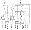
- FIGURES 7 and 8 are timing diagrams useful for explaining the generation of the display format shown in FIGURE 1(d), using fully cropped signals.
- FIGURE 9 is a block diagram of a circuit for generating the internal 2f H signal in the 1f H to 2f H conversion.
- FIGURE 10 is a combination block and circuit diagram for the deflection circuit shown in FIGURE 2.
- FIGURE 11 is a block diagram of the RGB interface shown in FIGURE 2.
- FIGURE 12 is a block diagram showing the auxiliary signal path and a portion of the main signal path in more detail.
- FIGURE 13 is a diagram of a five line FIFO line memory useful for explaining avoidance of read/write pointer collisions.
- FIGURE 14 is a block diagram of a simplified circuit for implementing an auxiliary synchronizing circuit for the gate array.
- FIGURE 15 is a timing diagram illustrating the correspondence of an upper/lower field indicator to the horizontal lines of a video frame.
- FIGURES 16-18 are useful for explaining a method for maintaining interlace integrity for simultaneously displayed video signals exhibiting relative precession.
- FIGURES 19(a)-19(b) are waveforms useful for explaining the operation of the circuit shown in FIGURE 20.
- FIGURE 20 is a block diagram of a circuit for maintaining interlace integrity as explained in connection with FIGURES 16-18.
- FIGURE 1 illustrate some, but not all of the various combinations of single and multiple picture display formats which can be implemented according to different inventive arrangements. Those selected for illustration are intended to facilitate the description of particular circuits comprising wide screen televisions according to the inventive arrangements. For purposes of convenience in illustration and discussion herein, a conventional display format ratio of width to height for a video source or signal is generally deemed to be 4 X 3, whereas a wide screen display format ratio of width to height for a video source or signal is generally deemed to be 16 X 9. The inventive arrangements are not limited by these definitions.
- FIGURE 1(a) illustrates a television, direct view or projection, having a conventional format display ratio of 4 X 3.
- a 16 X 9 format display ratio picture is transmitted, as a 4 X 3 format display ratio signal, black bars appear at the top and at the bottom.
- This is commonly referred to as letterbox format.
- the viewed picture is rather small with respect to the entire available display area.
- the 16 X 9 format display ratio source is converted prior to transmission, so that it will fill the vertical extent of a viewing surface of 4 X 3 format display. However, much information will be cropped from the left and/or right sides.
- the letterbox picture can be expanded vertically but not horizontally, whereby the resulting picture will evidence distortion by vertical elongation. None of the three alternatives is particularly appealing.
- FIGURE 1(b) shows a 16 X 9 screen.
- a 16 X 9 format display ratio video source would be fully displayed, without cropping and without distortion.
- a 16 X 9 format display ratio letterbox picture which is itself in a 4 X 3 format display ratio signal, can be progressively scanned by line doubling or line addition, so as to provide a larger display with sufficient vertical resolution.
- a wide screen television in accordance with this invention can display such a 16 X 9 format display ratio signal whether the main source, the auxiliary source or an external RGB source.
- FIGURE 1(c) illustrates a 16 X 9 format display ratio main signal in which a 4 X 3 format display ratio inset picture is displayed. If both the main and auxiliary video signals are 16 X 9 format display ratio sources, the inset picture can also have a 16 X 9 format display ratio. The inset picture can be displayed in many different positions.
- FIGURE 1(d) illustrates a display format, wherein the main and auxiliary video signals are displayed with the same size picture.
- Each display area has an format display ratio of 8 X 9, which is of course different from both 16 X 9 and 4 X 3.
- the signal In order to show a 4 X 3 format display ratio source in such a display area, without horizontal or vertical distortion, the signal must be cropped on the left and/or right sides. More of the picture can be shown, with less cropping, if some aspect ratio distortion by horizontal squeezing of the picture is tolerated. Horizontal squeezing results in vertical elongation of objects in the picture.
- the wide screen television according to this invention can provide any mix of cropping and aspect ratio distortion from maximum cropping with no aspect ratio distortion to no cropping with maximum aspect ratio distortion.
- FIGURE 1(e) is a display format wherein a 4 X 3 format display ratio picture is displayed in the center of a 16 X 9 format display ratio screen. Dark bars are evident on the right and left sides.
- FIGURE 1(f) illustrates a display format wherein one large 4 X 3 format display ratio picture and three smaller 4 X 3 format display ratio pictures are displayed simultaneously.
- a smaller picture outside the perimeter of the large picture is sometimes referred to as a POP, that is a picture-outside-picture, rather than a PIP, a picture-in-picture.
- POP picture-outside-picture
- PIP picture-in-picture
- tuners and additional auxiliary signal processing paths can provide for more than two moving pictures. It will also be appreciated that the large picture on the one hand, and the three small pictures on the other hand, can be switched in position, as shown in FIGURE 1(g).
- FIGURE 1(h) illustrates an alternative wherein the 4 X 3 format display ratio picture is centered, and six smaller 4 X 3 format display ratio pictures are displayed in vertical columns on either side.
- a wide screen television provided with two tuners can provide two moving pictures. The remaining eleven pictures will be in freeze frame format.
- FIGURE 1(i) shows a display format having a grid of twelve 4 X 3 format display ratio pictures.
- Such a display format is particularly appropriate for a channel selection guide, wherein each picture is at least a freeze frame from a different channel.
- the number of moving pictures will depend upon the number of available tuners and signal processing paths.
- FIGURE 1 The various formats shown in FIGURE 1 are illustrative, and not limiting, and can be implemented by wide screen televisions shown in the remaining drawings and described in detail below.
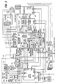
- FIGURE 2 An overall block diagram for a wide screen television in accordance with inventive arrangements, and adapted to operate with 2f H horizontal scanning, is shown in FIGURE 2 and generally designated 10.
- the television 10 generally comprises a video signals input section 20, a chassis or TV microprocessor 216, a wide screen processor 30, a 1f H to 2f H converter 40, a deflection circuit 50, an RGB interface 60, a YUV to RGB converter 240, kine drivers 242, direct view or projection tubes 244 and a power supply 70.
- the grouping of various circuits into different functional blocks is made for purposes of convenience in description, and is not intended as limiting the physical position of such circuits relative to one another.
- the video signals input section 20 is adapted for receiving a plurality of composite video signals from different video sources.
- the video signals may be selectively switched for display as main and auxiliary video signals.
- An RF switch 204 has two antenna inputs ANT1 and ANT 2. These represent inputs for both off-air antenna reception and cable reception.
- the RF switch 204 controls which antenna input is supplied to a first tuner 206 and to a second tuner 208.
- the output of first tuner 206 is an input to a one-chip 202, which performs a number of functions related to tuning, horizontal and vertical deflection and video controls.
- the particular one-chip shown is industry designated type TA7730.
- the baseband video signal VIDEO OUT developed in the one-chip and resulting from the signal from first tuner 206 is an input to both video switch 200 and the TV1 input of wide screen processor 30.
- Other baseband video inputs to video switch 200 are designated AUX1 and AUX 2. These might be used for video cameras, laser disc players, video tape players, video games and the like.
- the output of the video switch 200, which is controlled by the chassis or TV microprocessor 216 is designated SWITCHED VIDEO.
- the SWITCHED VIDEO is another input to wide screen processor 30.
- a switch SW1 wide screen processor selects between the TV1 and SWITCHED VIDEO signals as a SEL COMP OUT video signal which is an input to a Y/C decoder 210.
- the Y/C decoder 210 may be implemented as an adaptive line comb filter.
- Two further video sources S1 and S2 are also inputs to the Y/C decoder 210.
- Each of S1 and S2 represent different S-VHS sources, and each consists of separate luminance and chrominance signals.
- a switch which may be incorporated as part of the Y/C decoder, as in some adaptive line comb filters, or which may be implemented as a separate switch, is responsive to the TV microprocessor 216 for selecting one pair of luminance and chrominance signals as outputs designated Y_M and C_IN respectively.
- the selected pair of luminance and chrominance signals is thereafter considered the main signal and is processed along a main signal path.
- Signal designations including _M or _MN refer to the main signal path.
- the chrominance signal C_IN is redirected by the wide screen processor back to the one-chip, for developing color difference signals U_M and V_M.
- U is an equivalent designation for (R-Y)
- V is an equivalent designation for (B-Y).
- the Y_M, U_M, and V_M signals are converted to digital form in the wide screen processor for further signal processing.
- the second tuner 208 functionally defined as part of the wide screen processor 30, develops a baseband video signal TV2.
- a switch SW2 selects between the TV2 and SWITCHED VIDEO signals as an input to a Y/C decoder 220.
- the Y/C decoder 220 may be implemented as an adaptive line comb filter.
- Switches SW3 and SW4 select between the luminance and chrominance outputs of Y/C decoder 220 and the luminance and chrominance signals of an external video source, designated Y_EXT and C_EXT respectively.
- the Y_EXT and C_EXT signals correspond to the S-VHS input S1.
- the Y/C decoder 220 and switches SW3 and SW4 may be combined, as in some adaptive line comb filters.
- the output of switches SW3 and SW4 is thereafter considered the auxiliary signal and is processed along an auxiliary signal path.
- the selected luminance output is designated Y_A.
- Signal designations including _A, _AX and _AUX refer to the auxiliary signal path.
- the selected chrominance is converted to color difference signals U_A and V_A,
- the Y_A, U_A and V_A signals are converted to digital form for further signal processing.
- the arrangement of video signal source switching in the main and auxiliary signal paths maximizes flexibility in managing the source selection for the different parts of the different picture display formats.
- a composite synchronizing signal COMP SYNC, corresponding to Y_M is provided by the wide screen processor to a sync separator 212.
- the horizontal and vertical synchronizing components H and V respectively are inputs to a vertical countdown circuit 214.
- the vertical countdown circuit develops a VERTICAL RESET signal which is directed into the wide screen processor 30.
- the wide screen processor generates an internal vertical reset output signal INT VERT RST OUT directed to the RGB interface 60.
- a switch in the RGB interface 60 selects between the internal vertical reset output signal and the vertical synchronizing component of the external RGB source. The output of this switch is a selected vertical synchronizing component SEL_VERT_SYNC directed to the deflection circuit 50.
- Horizontal and vertical synchronizing signals of the auxiliary video signal are developed by sync separator 250 in the wide screen processor.
- the 1f H to 2f H converter 40 is responsible for converting interlaced video signals to progressively scanned noninterlaced signals, for example one wherein each horizontal line is displayed twice, or an additional set of horizontal lines is generated by interpolating adjacent horizontal lines of the same field. In some instances, the use of a previous line or the use of an interpolated line will depend upon the level of movement which is detected between adjacent fields or frames.
- the converter circuit 40 operates in conjunction with a video RAM 420.
- the video RAM may be used to store one or more fields of a frame, to enable the progressive display.
- the converted video data as Y_2f H , U_2f H and V_2f H signals is supplied to the RGB interface 60.
- the RGB interface 60 shown in more detail in FIGURE 11, enables selection of the converted video data or external RGB video data for display by the video signals input section.
- the external RGB signal is deemed to be a wide format display ratio signal adapted for 2f H scanning.
- the vertical synchronizing component of the main signal is supplied to the RGB interface by the wide screen processor as INT VERT RST OUT, enabling a selected vertical sync (f Vm or f Vext ) to be available to the deflection circuit 50. Operation of the wide screen television enables user selection of an external RGB signal, by generating an internal/external control signal INT/EXT.
- the RGB interface circuit detects an external synchronizing signal, in order to override the selection of a non-existent external RGB input.
- the WSP microprocessor 340 also supplies color and tint controls for the external RGB signal.
- the wide screen processor 30 comprises a picture in picture processor 320 for special signal processing of the auxiliary video signal.
- the term picture-in-picture is sometimes abbreviated as PIP or pix-in-pix.
- a gate array 300 combines the main and auxiliary video signal data in a wide variety of display formats, as shown by the examples of FIGURES 1(b) through 1(i).
- the picture-in-picture processor 320 and gate array 300 are under the control of a wide screen microprocessor (WSP ⁇ P) 340.
- Microprocessor 340 is responsive to the TV microprocessor 216 over a serial bus.
- the serial bus includes four signal lines, for data, clock signals, enable signals and reset signals.
- the wide screen processor 30 also generates a composite vertical blanking/reset signal, as a three level sandcastle signal.
- the vertical blanking and reset signals can be generated as separate signals.
- a composite blanking signal is supplied by the video signal input section to the RGB interface.
- the deflection circuit 50 receives a vertical reset signal from the wide screen processor, a selected 2f H horizontal synchronizing signal from the RGB interface 60 and additional control signals from the wide screen processor. These additional control signals relate to horizontal phasing, vertical size adjustment and east-west pin adjustment.
- the deflection circuit 50 supplies 2f H flyback pulses to the wide screen processor 30, the 1f H to 2f H converter 40 and the YUV to RGB converter 240.
- Operating voltages for the entire wide screen television are generated by a power supply 70 which can be energized by an AC mains supply.
- the wide screen processor 30 is shown in more detail in FIGURE 3.
- the principal components of the wide screen processor are a gate array 300, a picture-in-picture circuit 301, analog to digital and digital to analog converters, the second tuner 208, a wide screen processor microprocessor 340 and a wide screen output encoder 227. Further details of the wide screen processor are shown in FIGURE 4.
- the gate array 300 is shown in more detail in FIGURE 6. A number of the components shown in FIGURE 3 have already been described in detail.
- the second tuner 208 has associated therewith an IF stage 224 and an audio stage 226.
- the second tuner 208 also operates in conjunction with the WSP ⁇ P 340.
- the WSP ⁇ P 340 comprises an input output I/O section 340A and an analog output section 340B.
- the I/O section 340A provides tint and color control signals, the INT/EXT signal for selecting the external RGB video source and control signals for the switches SW1 through SW6.
- the I/O section also monitors the EXT SYNC DET signal from the RGB interface to protect the deflection circuit and cathode ray tube(s).
- the analog output section 340B provides control signals for vertical size, east-west adjust and horizontal phase, through respective interface circuits 254, 256 and 258.
- the gate array 300 is responsible for combining video information from the main and auxiliary signal paths to implement a composite wide screen display, for example one of those shown in the different parts of FIGURE 1.
- Clock information for the gate array is provided by phase locked loop 374, which operates in conjunction with low pass filter 376.
- the main video signal is supplied to the wide screen processor in analog form, and Y U V format, as signals designated Y_M, U_M and V_M. These main signals are converted from analog to digital form by analog to digital converters 342 and 346, shown in more detail in FIGURE 4.
- the color component signals are referred to by the generic designations U and V, which may be assigned to either R-Y or B-Y signals, or I and Q signals.
- the sampled luminance bandwidth is limited to 8 MHz because the system clock rate is 1024f H , which is approximately 16 MHz.
- a single analog to digital converter and an analog switch can be used to sample the color component data because the U and V signals are limited to 500 KHz, or 1.5 MHz for wide l.
- the select line UV_MUX for the analog switch, or multiplexer 344 is an 8 MHz signal derived by dividing the system clock by 2.
- a one clock wide start of line SOL pulse synchronously resets this signal to zero at the beginning of each horizontal video line.
- the UV_MUX line than toggles in state each clock cycle through the horizontal line.
- the state of the UV_MUX since the line length is an even number of clock cycles, the state of the UV_MUX, once initialized, will consistently toggle 0, 1, 0, 1, ..., without interruption.
- the Y and UV data streams out of the analog to digital converters 342 and 346 are shifted because the analog to digital converters each have 1 clock cycle of delay.
- the clock gating information from the main signal processing path 304 must be similarly delayed. Were the clock gating information not delayed, the UV data will not be correctly paired when deleted. This is important because each UV pair represents one vector. A U element from one vector cannot be paired with a V element from another vector without causing a color shift. Instead, a V sample from a previous pair will be deleted along with the current U sample.
- This method of UV multiplexing is referred to as 2:1:1, as there are two luminance samples for every pair of color component (U, V) samples.
- the Nyquist frequency for both U and V is effectively reduced to one half of the luminance Nyquist frequency. Accordingly, the Nyquist frequency of the output of the analog to digital converter for the luminance component is 8 MHz, whereas the Nyquist frequency of the output of the analog to digital converter for the color components is 4 MHz.
- the PIP circuit and/or the gate array may also include means for enhancing the resolution of the auxiliary data notwithstanding the data compression.
- a number of data reduction and data restoration schemes have been developed, including for example paired pixel compression and dithering and dedithering. Moreover, different dithering sequences involving different numbers of bits and different paired pixel compressions involving different numbers of bits are contemplated.
- One of a number of particular data reduction and restoration schemes can be selected by the WSP ⁇ P 340 in order to maximize resolution of the displayed video for each particular kind of picture display format.
- the gate array includes interpolators which operate in conjunction with line memories, which may be implemented as FIFO's 356 and 358.
- the interpolator and FIFO's are utilized to resample the main signal as desired.
- An additional interpolator can resample the auxiliary signal.
- Clock and synchronizing circuits in the gate array control the data manipulation of both the main and auxiliary signals, including the combination thereof into a single output video signal having Y_MX, U_MX and V_MX components. These output components are converted to analog form by digital to analog converters 360, 362 and 364.
- the analog form signals, designated Y, U and V are supplied to the 1f H to 2f H converter 40 for conversion to noninterlaced scanning.
- the Y, U and V signals are also encoded to Y/C format by encoder 227 to define a wide format ratio output signal Y_OUT_EXT/C_OUT_EXT available at panel jacks.
- Switch SW5 selects a synchronizing signal for the encoder 227 from either the gate array, C_SYNC_MN, or from the PIP circuit, C_SYNC_AUX.
- Switch SW6 selects between Y_M and C_SYNC_AUX as synchronizing signal for the wide screen panel output.
- Phase comparator 228 is part of a phase locked loop including low pass filter 230, voltage controlled oscillator 232, divider 234 and capacitor 236.
- the voltage controlled oscillator 232 operates at 32f H , responsive to a ceramic resonator or the like 238.
- the output of the voltage controlled oscillator is divided by 32 to provide a proper frequency second input signal to phase comparator 228.
- the output of the divider 234 is a 1f H REF timing signal.
- the 32f H REF and 1f H REF timing signals are supplied to a divide by 16 counter 400.
- a 2f H output is supplied to a pulse width circuit 402.
- Presetting divider 400 by the 1f H REF signal assures that the divider operates synchronously with the phase locked loop of the video signals input section.
- Pulse width circuit 402 assures that a 2f H -REF signal will have an adequate pulse width to assure proper operation of the phase comparator 404, for example a type CA1391, which forms part of a second phase locked loop including low pass filter 406 and 2f H voltage controlled oscillator 408.
- Voltage controlled oscillator 408 generates an internal 2f H timing signal, which is used for driving the progressively scanned display.
- the other input signal to phase comparator 404 is the 2f H flyback pulses or a timing signal related thereto.
- phase locked loop including phase comparator 404 is useful for assuring that each 2f H scanning period is symmetric within each 1f H period of the input signal. Otherwise, the display may exhibit a raster split, for example, wherein half of the video lines are shifted to the right and half of the video lines are shifted to the left.
- the deflection circuit 50 is shown in more detail in FIGURE 10.
- a circuit 500 is provided for adjusting the vertical size of the raster, in accordance with a desired amount of vertical overscan necessary for implementing different display formats.
- a constant current source 502 provides a constant quantity of current I RAMP which charges a vertical ramp capacitor 504.
- a transistor 506 is coupled in parallel with the vertical ramp capacitor, and periodically discharges the capacitor responsive to the vertical reset signal.
- current I RAMP provides the maximum available vertical size for the raster. This might correspond to the extent of vertical overscan needed to fill the wide screen display by an expanded 4 X 3 format display ratio signal source, as shown in FIGURE 1(a).
- an adjustable current source 508 diverts a variable amount of current I ADJ from I RAMP , so that vertical ramp capacitor 504 charges more slowly and to a smaller peak value.
- Variable current source 508 is responsive to a vertical size adjust signal, for example in analog form, generated by a vertical size control circuit.
- Vertical size adjustment 500 is independent of a manual vertical size adjustment 510, which may be implemented by a potentiometer or back panel adjustment knob. In either event, the vertical deflection coil(s) 512 receive(s) driving current of the proper magnitude.
- Horizontal deflection is provided by phase adjusting circuit 518, East-West pin correction circuit 514, a 2f H phase locked loop 520 and horizontal output circuit 516.
- the RGB interface circuit 60 is shown in more detailed in FIGURE 11.
- the signal which is to be ultimately displayed will be selected between the output of the 1f H to 2f H converter 40 and an external RGB input.
- the external RGB input is presumed to be a wide format display ratio, progressively scanned source.
- the external RGB signals and a composite blanking signal from the video signals input section 20 are inputs to an RGB to Y U V converter 610.
- the external 2f H composite synchronizing signal for the external RGB signal is an input to external synchronizing signal separator 600.
- Selection of the vertical synchronizing signal is implemented by switch 608.
- Selection of the horizontal synchronizing signal is implemented by switch 604.
- Selection of the video signal is implemented by switch 606.
- Each of the switches 604, 606 and 608 is responsive to an internal/external control signal generated by the WSP ⁇ P 340.
- Selection of internal or external video sources is a user selection. However, if a user inadvertently selects an external RGB source, when no such source is connected or turned on, or if the external source drops out, the vertical raster will collapse, and serious damage to the cathode ray tube(s) can result. Accordingly, an external synchronizing detector 602 checks for the presence of an external synchronizing signal. In the absence of such a signal, a switch override control signal is transmitted to each of switches 604, 606 and 608, to prevent selection of the external RGB source if the signal therefrom is not present.
- the RGB to YUV converter 610 also receives tint and color control signals from the WSP ⁇ P 340.
- FIGURE 4 is a block diagram showing further details of the wide screen processor 30 shown in FIGURE 3.
- the Y_A, U_A and V_A signals are an input to the picture in picture processor 320, which can include a resolution processing circuit 370.
- the wide screen television according to aspects of this invention can expand and compress video.
- the special effects embodied by the various composite display formats illustrated in part in FIGURE 1 are generated by the picture-in-picture processor 320, which can receive resolution processed data signals Y_RP, U_RP and V_RP from resolution processing circuit 370. Resolution processing need not be utilized at all times, but during selected display formats.
- the picture-in-picture processor 320 is shown in more detail in FIGURE 5.
- the principal components of the picture-in-picture processor are an analog-to-digital converter section 322, an input section 324, a fast switch (FSW) and bus section 326, a timing and control section 328 and a digital-to-analog converter section 330.
- analog-to-digital converter section 322 an input section 324, a fast switch (FSW) and bus section 326, a timing and control section 328 and a digital-to-analog converter section 330.
- FSW fast switch
- the picture-in-picture processor 320 may be embodied as an improved variation of a basic CPIP chip developed by Thomson Consumer Electronics, Inc.
- the basic CPIP chip is described more fully in a publication entitled The CTC 140 Picture in Picture (CPIP) Technical Training Manual, available from Thomson Consumer Electronics, Inc., Indianapolis, Indiana.
- the basic special effect is a large picture having a small picture overlaying a portion thereof as shown in FIGURE 1(c).
- the large and small pictures can result from the same video signal, from different video signals and can be interchanged or swapped. Generally speaking, the audio signal is switched to always correspond to the big picture.
- the small picture can be moved to any position on the screen or can step through a number of predetermined positions.
- a zoom feature increases and decreases the size of the small picture, for example to any one of a number of preset sizes.
- the large and small pictures are in fact the same size.
- a user can zoom in on the content of the single picture, for example, in steps from a ratio of 1.0:1 to 5.0:1. While in the zoom mode a user may search or pan through the picture content enabling the screen image to move across different areas of the picture. In either event, either the small picture or the large picture or the zoomed picture can be displayed in freeze frame (still picture format). This function enables a strobe format, wherein the last nine frames of video can be repeated on the screen. The frame repetition rate can be changed from thirty frames per second to zero frames per second.
- the picture-in-picture processor used in the wide screen television differs from the present configuration of the basic CPIP chip described above. If the basic CPIP chip were used with a television having a 16 X 9 screen, and without a video speed up circuit, the inset pictures would exhibit aspect ratio distortion, due to the effective 4/3 times horizontal expansion resulting from scanning across the wider 16 X 9 screen. Objects in the picture would be horizontally elongated. If an external speed up circuit were utilized, there would be no aspect ratio distortion, but the picture would not fill the entire screen.
- the picture-in-picture processor 320 is adapted for asymmetrically compressing the video data in one of a plurality of selectable display modes.
- this mode of operation the pictures are compressed 4:1 in the horizontal direction and 3:1 in the vertical direction.
- This asymmetric mode of compression produces aspect ratio distorted pictures for storage in the video RAM. Objects in the pictures are squeezed horizontally. However, if these pictures are read out normally, as for example in the channel scan mode, for display of a 16 X 9 format display ratio screen, the pictures appear correct. The picture fills the screen and there is no aspect ratio distortion.
- the asymmetric compression mode according to this aspect of the invention makes it possible to generate the special display formats on a 16 X screen without external speed up circuitry.
- the picture-in-picture processor in conjunction with a free running oscillator 348 will take Y/C input from a decoder, for example an adaptive line comb filter, decode the signal into Y, U, V color components and generate horizontal and vertical sync pulses.
- a decoder for example an adaptive line comb filter
- These signals are processed in the picture-in-picture processor for the various full screen modes such as zoom, freeze and channel scan.
- the horizontal and vertical sync present from the video signals input section will have many discontinuities because the signals sampled (different channels) will have non-related sync pulses and will be switched at seemingly random moments in time. Therefore the sample clock (and read/write video RAM clock) is determined by the free running oscillator.
- the sample clock will be locked to incoming video horizontal sync, which in these special cases is the same as the display clock frequency.
- Y, U, V and C_SYNC composite sync outputs from the picture-in-picture processor in analog form can be re-encoded into Y/C components by encode circuit 366, which operates in conjunction with a 3.58 MHz oscillator 380.
- This Y/C_PIP_ENC signal may be connected to a Y/C switch, not shown, which enables the re-encoded Y/C components to be substituted for the Y/C components of the main signal.
- the PIP encoded Y, U, V and sync signals would be the basis for horizontal and vertical timing in the rest of the chassis. This mode of operation is appropriate for implementing a zoom mode for the PIP, based upon operation of the interpolator and FIFO's in the main signal path.
- the picture-in-picture processor 320 comprises analog to digital converting section 322, input section 324, fast switch FSW and bus control section 326, timing and control section 328 and digital to analog converting section 330.
- the picture-in-picture processor 320 digitizes the video signal into luminance (Y) and color difference signals (U, V), subsampling and storing the results in a 1 megabit video RAM 350 as explained above.
- the video RAM 350 associated with the picture-in-picture processor 320 has a memory capacity of 1 megabit, which is not large enough to store a full field of video data with 8-bit samples. Increased memory capacity tends to be expensive and can require more complex management circuitry.
- the smaller number of bits per sample in the auxiliary channel represents a reduction in quantization resolution, or bandwidth, relative to the main signal, which is processed with 8-bit samples throughout.
- This effective reduction of bandwidth is not usually a problem when the auxiliary displayed picture is relatively small, but can be troublesome if the auxiliary displayed picture is larger, for example the same size as the main displayed picture.
- Resolution processing circuit 370 can selectively implement one or more schemes for enhancing the quantization resolution or effective bandwidth of the auxiliary video data.
- a number of data reduction and data restoration schemes have been developed, including for example, paired pixel compression and dithering and dedithering.
- a dedithering circuit would be operatively disposed downstream of the video RAM 350, for example in the auxiliary signal path of the gate array, as explained in more detail below.
- the luminance and color difference signals of the auxiliary signal are stored in an 8:1:1 six-bit Y, U ,V fashion in a video RAM 350 forming part of the picture-in-picture processor.
- each component is quantized into six-bit samples.
- the picture-in-picture processor 320 is operated in a mode whereby incoming video data is sampled with a 640f H clock rate locked to the incoming auxiliary video synchronizing signal instead. In this mode, data stored in the video RAM 350 is orthogonally sampled. When the data is read out of the picture-in-picture processor video RAM 350, it is read using the same 640f H clock locked to the incoming auxiliary video signal.
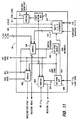
- the main signal path 304, auxiliary signal path 306 and output signal path 312 of the gate array 300 are shown in block diagram form in FIGURE 6.
- the gate array also comprises a clocks/sync circuit 320 and a WSP ⁇ P decoder 310. Data and address output lines of the WSP ⁇ P decoder 310, identified as WSP DATA, are supplied to each of the main circuits and paths identified above, as well as to the picture-in-picture processor 320 and resolution processing circuit 370. It will be appreciated that whether or not certain circuits are, or are not, defined as being part of the gate array is largely a matter of convenience for facilitating explanation of the inventive arrangements.
- the gate array is responsible for expanding, compressing and cropping video data of the main video channel, as and if necessary, to implement different picture display formats.
- the luminance component Y_MN is stored in a first in first out (FIFO) line memory 356 for a length of time depending on the nature of the interpolation of the luminance component.
- the combined chrominance components U/V_MN are stored in FIFO 358.
- Auxiliary signal luminance and chrominance components Y_PIP, U_PIP and V_PIP are developed by demultiplexer 355.
- the luminance component undergoes resolution processing, as desired, in circuit 357, and is expanded as necessary by interpolator 359, generating signal Y_AUX as an output.
- the auxiliary display will be as large as the main signal display, as shown for example in FIGURE 1(d).
- the memory limitations associated with the picture-in-picture processor and video RAM 350 can provide an insufficient number of data points, or pixels for filling such a large display area.
- resolution processing circuit 357 can be used to restore pixels to the auxiliary video signal to replace those lost during data compression, or reduction.
- the resolution processing may correspond to the resolution processing undertaken by circuit 370 shown in FIGURE 4.
- circuit 370 may be a dithering circuit and circuit 357 may be a dedithering circuit.
- the auxiliary video input data is sampled at a 640f H rate and stored in video RAM 350.
- the auxiliary data is read out of video RAM 350 is designated VRAM_OUT.
- the PIP circuit 301 also has the capability of reducing the auxiliary picture by equal integer factors horizontally and vertically, as well as asymmetrically.
- the auxiliary channel data is buffered and synchronized to the main channel digital video by the 4 bit latches 352A and 352B, the auxiliary FIFO 354, timing circuit 369 and synchronization circuit 368.
- the VRAM_OUT data is sorted into Y (luminance), U, V (color components), and FSW_DAT (fast switch data) by demultiplexer 355.
- the FSW_DAT indicates which field type was written into the video RAM.
- the PIP_FSW signal is received directly from the PIP circuit and applied to the output control circuit 321 to determine which field read out of video RAM is to be displayed during the small picture modes.
- the auxiliary channel is sampled at 640f H rate while the main channel is sampled at a 1024f H rate.
- the auxiliary channel FIFO 354 converts the data from the auxiliary channel sample rate to the main channel clock rate.
- the video signal undergoes an 8/5 (1024/640) compression. This is more than the 4/3 compression necessary to correctly display the auxiliary channel signal. Therefore, the auxiliary channel must be expanded by the interpolator 359 to correctly display a 4 X 3 small picture.
- the interpolator 359 is controlled by interpolator control circuit 371, which is itself responsive to WSP ⁇ P 340.
- the amount of interpolator expansion required is 5/6.
- the chrominance components U_PIP and V_PIP are delayed by circuit 367 for a length of time depending on the nature of the interpolation of the luminance component, generating signals U_AUX and V_AUX as outputs.
- the respective Y, U and V components of the main and auxiliary signals are combined in respective multiplexers 315, 317 and 319 in the output signal path 312, by controlling the read enable signals of the FIFO's 354, 356 and 358.
- the multiplexers 315, 317 and 319 are responsive to output multiplexer control circuit 321.
- Output multiplexer control circuit 321 is responsive to a clock signal, a start of line signal, a horizontal line counter signal, the vertical blanking reset signal and the output of the fast switch from the picture-in-picture processor and WSP ⁇ P 340.
- the multiplexed luminance and chrominance components Y_MX, U_MX and V_MX are supplied to respective digital/analog converters 360, 362 and 364 respectively.
- the digital to analog converters are followed by low pass filters 361, 363 and 365 respectively, shown in FIGURE 4.
- the various functions of the picture-in-picture processor, the gate array and the data reduction circuit are controlled by WSP ⁇ P 340.
- the WSP ⁇ P 340 is responsive to the TV ⁇ P 216, being connected thereto by a serial bus.
- the serial bus may be a four wire bus as shown, having lines for data, clock signals, enable signals and reset signals.
- the WSP ⁇ P 340 communicates with the different circuits of the gate array through a WSP ⁇ P decoder 310.
- the video can be expanded to perform horizontal zooming operations usually accompanied by vertical zooming. Horizontal zoom operations up to 33% can be accomplished by reducing compressions to less than 4/3.
- a sample interpolator is used to recalculate the incoming video to a new pixel positions because the luminance video bandwidth, up to 5.5 MHz for S-VHS format, occupies a large percentage of the Nyquist fold over frequency, which is 8 MHz for a 1024f H clock.
- the luminance data Y_MN is routed through an interpolator 337 in the main signal path 304 which recalculates sample values based on the compression or the expansion of the video.
- the function of the switches or route selectors 323 and 331 is to reverse the topology of the main signal path 304 with respect to the relative positions of the FIFO 356 and the interpolator 337. In particular, these switches select whether the interpolator 337 precedes the FIFO 356, as required for picture compression, or whether the FIFO 356 precedes the interpolator 337. as required for picture expansion.
- the switches 323 and 331 are responsive to a route control circuit 335, which is itself responsive to the WSP ⁇ P 340. It will be remembered that the auxiliary video signal is compressed for storage in the video RAM 350, and only expansion is necessary for practical purposes. Accordingly, no comparable switching is required in the auxiliary signal path.
- every fourth sample can be inhibited from being written into the FIFO 356.
- the write enable signal has clock gating information attached to it in the form of inhibit pulses. For expanding data, the clock gating information is applied to the read enable signal. This will pause the data as it is being read from the FIFO 356.
- the interpolator 337 which follows the FIFO 356 during this process, to recalculate the sampled data from jagged to smooth.
- the data In the expansion case the data must pause while being read from the FIFO 356 and while being clocked into the interpolator 337. This is different from the compression case where the data is continuously clocked through the interpolator 337.
- the clock gating operations can easily be performed in a synchronous manner, that is, events can occur based on the rising edges of the system clock 1024f H .
- the PIP circuit 301 manipulates a 6 bit Y, U, V, 8:1:1 field memory, video RAM 350, to store incoming video data.
- the video RAM 350 holds two fields of video data in a plurality of memory locations. Each memory location holds eight bits of data. In each 8-bit location there is one 6-bit Y (luminance) sample (sampled at 640f H ) and 2 other bits. These two other bits hold either fast switch data (FSW_DAT) or part of a U or V sample (sampled at 80f H ).
- the FSW_DAT values indicate which type of field was written into video RAM.
- the PIP circuit 301 will determine which field will be read out of the memory to be displayed through the use of the fast switch data. The PIP circuit always reads the opposite field type that is being written to overcome a motion tear problem. If the field type being read is the opposite type than that being displayed, then the even field stored in the video RAM is inverted by deleting the top line of the field when the field is read out of memory. The result is that the small picture maintains correct interlace without a motion tear.
- the clocks/sync circuit 320 generates read, write and enable signals needed for operating FIFOs 354, 356 and 358.
- the FIFOs for the main and auxiliary channels are enabled for writing data into storage for those portions of each video line which is required for subsequent display. Data is written from one of the main or auxiliary channels, but not both, as necessary to combine data from each source on the same video line or lines of the display.
- the FIFO 354 of the auxiliary channel is written synchronously with the auxiliary video signal, but is read out of memory synchronously with the main video signal.
- the main video signal components are read into the FIFOs 356 and 358 synchronously with the main video signal, and are read out of memory synchronously with the main video. How often the read function is switched back and forth between the main and auxiliary channels is a function of the particular special effect chosen.
- FIGURES 7 and 8 The process for this display format is illustrated in FIGURES 7 and 8.
- each of the FIFOs the video data is buffered to be read out at a particular point in time.
- the active region of time where the data may be read out from each FIFO is determined by the display format chosen.
- the main channel video is being displayed on the left hand half of the display and the auxiliary channel video is displayed on the right hand half of the display.
- the arbitrary video portions of the waveforms are different for the main and auxiliary channels as illustrated.
- the read enable control signal (RD_EN_MN) of the main channel 910 x 8 FIFOs is active for 50% of the display active line period of the display beginning with the start of active video, immediately following the video back porch.
- auxiliary channel read enable control signal (RD_EN_AX) is active for the other 50% of the display active line period beginning with the falling edge of the RD_EN_MN signal and ending with the beginning of the main channel video front porch. It may be noted that write enable control signals are synchronous with their respective FIFO input data (main or auxiliary) while the read enable control signals are synchronous with the main channel video.
- the display format shown in FIGURE 1(d) is particularly desirable as it enables two nearly full field pictures to displayed in a side by side format.
- the display is particularly effective and appropriate for a wide format display ratio display, for example 16 X 9.
- Most NTSC signals are represented in a 4 X 3 format, which of course corresponds to 12 x 9.
- Two 4 X 3 format display ratio NTSC pictures may be presented on the same 16 X 9 format display ratio display, either by cropping the pictures by 33% or squeezing the pictures by 33%, and introducing aspect ratio distortion.
- the ratio of picture cropping to aspect ratio distortion may be set any where in between the limits of 0% and 33%
- two side by side pictures may be presented as 16.7 % squeezed and 16.7% cropped.
- the horizontal display time for a 16 X 9 format display ratio display is the same as a 4 X 3 format display ratio display, because both have 62.5 microsecond nominal line length. Accordingly, an NTSC video signal must be sped up by a factor of 4/3 to preserve a correct aspect ratio, without distortion.
- Variable interpolators are utilized in accordance with aspects of this invention to speed up the video signals. In the past, FIFOs having different clock rates at the inputs and outputs have been used to perform a similar function.
- each picture must be distorted or cropped, or some combination thereof, by 50%. A speed up comparable to that needed for a wide screen application is unnecessary.
- the video display and deflection system is synchronized with the main video signal.
- the main video signal must be speeded up, as explained above, to fill the wide screen display.
- the auxiliary video signal must be vertically synchronized with the first video signal and the video display.
- the auxiliary video signal can be delayed by a fraction of a field period in a field memory, and then expanded in a line memory. Synchronization of the auxiliary video data with main video data is accomplished by utilizing the video RAM 350 as a field memory and a first in first out (FIFO) line memory device 354 for expanding the signal.
- FIFO first in first out
- the picture-in-picture processor operates in such a manner that the auxiliary video data is sampled with a 640f H clock locked to the horizontal synchronizing component of the incoming auxiliary video signal.
- This operation enables orthogonally sampled data to be stored in the video RAM 350. Data must be read out of the video RAM at the same 640f H rate. The data cannot be orthogonally displayed from the video RAM without modification due to the generally asynchronous nature of the main and auxiliary video sources.
- a line memory with independent write and read port clocks is disposed in the auxiliary signal path after the output of the video RAM 350.
- the output of the video RAM 350 is an input to the first of two 4-bit latches 352A and 352B.
- the VRAM_OUT output is in 4-bit data blocks.
- the 4-bit latches are used to recombine the auxiliary signal back into 8-bit data blocks.
- the latches also reduce the data clock rate from 1280f H to 640f H .
- the 8-bit data blocks are written into the FIFO 354 by the same 640f H clock used to sample the auxiliary video data for storage in the video RAM 350.
- the size of FIFO 354 is 2048 X 8.
- the 8-bit data blocks are read out of the FIFO 354 by the 1024f H display clock, which is locked to the horizontal synchronizing component of the main video signal.
- This basic configuration which uses a multiple line memory with independent read and write port clocks, enables data which was orthogonally sampled to be displayed orthogonally.
- the 8-bit data blocks are divided into 6-bit luminance and color difference samples by demultiplexer 355.
- the data samples may then be interpolated as necessary for the desired format display ratio and written as video data output.
- An aspect of the invention recognizes that precession rates greater than 2 lines/field are not likely to be encountered. Therefore, a design criteria of a 5 line FIFO for the auxiliary channel can be sufficient to prevent read/write pointer collisions.
- FIGURE 13 A block diagram for a simplified circuit formed by D-type flip/flops for generating line delays (Z -1 ) and reset pulses for controlling writing and reading in the FIFO 354 in the auxiliary signal path is shown in FIGURE 14.
- This reset pulse denoted WR_RST_AX is the combination of V_SYNC_MN sampled by H_SYNC_AX.
- WR_RST_AX occurs at the first horizontal synchronizing pulse of the auxiliary video signal which occurs after a vertical synchronizing pulse of the main signal.
- RD_RST_AX occurs at the third horizontal synchronizing pulse of the main video signal which occurs after a vertical synchronizing pulse of the main signal, or stated still otherwise, at the second horizontal synchronizing pulse of the main signal which occurs after the WR_RST_AX pulse.
- the main and auxiliary signals are asynchronous, there is some ambiguity about exactly where the write pointer is when the read pointer is reset. It is known that the write pointer is leading the read pointer by at least two lines. However, if the frequency of the auxiliary channel horizontal sync is higher than the frequency of the main channel horizontal sync, then the write pointer will have advanced past the 2 line marker shown. It is in this way that a pointer collision is avoided for all signals with less than 2 lines/field precession rate.
- the auxiliary channel FIFO 354 is partitioned into 5 line pieces through appropriately timed read and write reset signals. In this scheme, the read and write pointers are initialized at the beginning of each displayed field at least 2 lines apart from each other.
- the sacrifice always comes at the expense of allowing the read pointer to catch up with the write pointer.
- only 80% of the video line is considered active because the picture-in-picture processor is not capable of storing more than 512 video samples in the video RAM 350. In practice, this still provides a good active video line. In these cases, the precession rate is being sacrificed for more visible picture content. In addition, there is more distortion in the auxiliary video. In the worst case, up to one line per field of precession can be tolerated between the main and auxiliary video sources. This is still more than is necessary for most video sources, and the precession rate tolerance is sacrificed on those feature modes which can be expected to be the least used.
- Another problem stemming from the asynchronous reading and writing of the FIFO is that of maintaining interlace integrity of the auxiliary channel video. Since the display is locked to the main channel video, the current field type being displayed, that is the upper or lower field, will be determined by the main signal.
- the field type which is stored in the video RAM 350 memory and ready to be read out at the start of the main channel field may or may not be the same as the displayed field type. It may be necessary to change the auxiliary field type stored in the video RAM 350 to match that of the main channel display.
- the picture-in-picture processor 320 and the gate array 300 quantize 262.5 line fields of the NTSC signal into 263 line upper fields (sometimes referred to odd fields) and 262 line lower fields (sometimes called even fields). This is due to fact that vertical sync is sampled with pulses representing horizontal sync. This is illustrated by the diagram of FIGURE 15.
- An upper/lower field type indicator has a value 1 for upper fields and a value 0 for lower fields.
- the upper fields include odd lines 1 through 263.
- the lower fields include even lines 2 through 262.
- the first field type indicator U/L MAIN SIGNAL represents the field type of the main video channel.
- the signal HSYNC_AX represents the horizontal sync signals for each line of the auxiliary channel.
- the field type indicator U/L(A) represents the field type stored in the video ram 350 if each auxiliary channel line were written in "normally".
- the term normal is used here to indicate that the odd lines 1-263 are written in to the video RAM 350 as the upper field is being received and decoded.
- the field type indicator U/L(B) represents the field type stored in the video RAM 350 if the first line of the upper field is not written into the video RAM 350 during the reception of an upper field. Instead, the first line is actually tacked onto the last line (number 262) of the lower field. This effectively inverts the field type since line 2 will be the first displayed line and line 3 will be the second displayed line in the frame. The received upper field now becomes the lower field and vice-versa.
- the field type indicator U/L(C) represents the field type stored in the video RAM 350 if the last line of the upper field is added to the video RAM 350 during the reception of the lower field. This effectively inverts the field type, since line 263 will be the first displayed line and line 1 will be the second displayed line.
- the U/L MAIN SIGNAL will shift to the left or the right with respect to the auxiliary channel U/L(A,B,C) field type indicators.
- data should be written into the video RAM 350 using mode A, because the decision edge is in zone A.
- Mode A is appropriate because when the picture-in-picture processor receives vertical sync, it will write the same field type into the video RAM 350 as will be required by the display to read from the video RAM 350 starting with V_SYNC_MN (main channel vertical sync).
- the mode will change according to their relative positions.
- the valid modes are shown graphically at the top of FIGURE 16 and in the table of FIGURE 17. There is an overlap between modes B and C, since most of the time that mode B is valid. mode C is also valid, and vice-versa. This is true for all but 2 lines out of 262 lines. Either of modes B or C can be utilized when both are valid.
- FIGURE 20 A block diagram of a circuit 700 for maintaining interlace integrity according to this inventive arrangement is shown in FIGURE 20.
- the output signals of circuit 700 are write and read reset control signals for the video RAM 350, the FIFO 354 in the auxiliary signal path and the FIFO 356 in the main signal path, as shown in FIGURE 12.
- the field type of the main video signal is determined from a pair of signals, VSYNC_MN AND HSYNC_MN.
- the field type of the auxiliary video signal is determined from a corresponding pair c' signals, VSYNC_AX AND HSYNC_AX.
- Each pair of signals has a predetermined phase relationship which is set in the gate array. This relationship is shown in FIGURES 19(a)-19(c), which apply to both pairs of signals.
- HSYNC is a square wave, whose rising edge corresponds to the start of a horizontal line of the respective signal.
- VSYNC has only one rising edge per field, which corresponds to the start of a vertical field of the respective signal.
- the relationship between the rising edges of the respective pairs of signals is tested by circuit 700 to determine what steps, if any, are necessary to match the field type of the auxiliary signal to the field type of the main signal.
- the leading edges of the main pair of signals are never closer than 1/8 of a horizontal line period.
- the leading edges of the auxiliary pair of signals are never closer than 1/10 of a horizontal line period. This prevents jitter of the leading edges relative to one another. This relationship is assured by the timing circuits in the gate array.
- the main signal pair VSYNC_MN and HSYNC_MN are inputs to a first field type circuit 702, which comprises two D-type flip/flops.
- HSYNC_MN is sampled by VSYNC_MN, that is, VSYNC_MN is the clock input.
- the output of this flip/flop is an upper/lower field indicator UL_MN for the main signal, which can be a logical HI for an upper field type and a logical LO for a lower field type, although this is arbitrary.
- VSYNC_MN is sampled by HSYNC_MN, just as in flip/flop 852 explained in connection with FIGURE 14. This provides an output V H , which is the vertical synchronized to the horizontal.
- the auxiliary signal pair VSYNC_AX and HSYNC_AX are inputs to a first field type circuit 710, which also comprises two D-type flip/flops.
- HSYNC_AX is sampled by VSYNC_AX, that is, VSYNC_AX is the clock input.
- the output of this flip/flop is an upper/lower field indicator UL_AX for the auxiliary signal, which can be a logical HI for an upper field type and a logical LO for a lower field type, although this is arbitrary.
- VSYNC_AX is sampled by HSYNC_AX, just as in flip/flop 852 explained in connection with FIGURE 14. This provides an output VH, which is the vertical synchronized to the horizontal.
- FIGURES 19(a)-19(c) The field type determination for both signals is shown in FIGURES 19(a)-19(c). If the rising start of field edge occurs in the first half of the horizontal line period, as in FIGURE 19(b), the field is a lower field type. If the rising start of field edge occurs in the second half of the horizontal line period, as in FIGURE 19(c), the field is an upper field type.
- the VH for the main signal and HSYNC_MN are inputs to delay circuits 704, 706 and 708, which provide horizontal line period delays to assure the proper phase relationship of the output signals WR_RST_FIFO_MN, RD_RST_FIFO_MN and RD_RST_FIFO_AX.
- the delay operation which can be implemented by D-type flip/flops, is similar to the circuit shown in FIGURE 14. Two to three horizontal line periods of delay are provided between the write and read pointers.
- the upper/lower field type indicator UL_MN corresponds to U/L MAIN SIGNAL shown at the top of FIGURE 16 and is one input to a UL_SEL comparator 714.
- the other inputs to comparator 714 are supplied by UL_AX test generator 712.
- Test generator 712 has the UL_AX field indicator as an input, as well as HSYNC_AX as a clock input.
- Test generator 712 provides signals U/L(A), U/L(B) and U/L(C) shown in the bottom of FIGURE 16, corresponding to the three possible modes A, B and C.
- Each of the signals U/L(A), U/L(B) and U/L(C) is compared with UL_MN, at the time of the decision edge of U/L_MN, also shown in FIGURE 16. If UL_MN matches U/L(A), the field types match and no action to maintain interlace integrity is necessary. If UL_MN matches U/L(B), the field types do not match. It is necessary to delay writing the upper field by one line to maintain interlace integrity. If UL_MN matches U/L(C), the field types do not match. It is necessary to advance writing the lower field by one line to maintain interlace integrity.
- RST_AX_SEL selector circuit 718 The results of this comparison are an input to RST_AX_SEL selector circuit 718.
- the other inputs are the three vertical synchronizing signals RST_A, RST_B and RST_C generated by RST_AX_GEN generator 716.
- the three vertical synchronizing signals RST_A, RST_B and RST_C have different phases relative to one another in order to implement the corrective action, or no corrective action, to maintain interlace integrity according to the output of the comparator 714.
- Delay circuit 722 resynchronizes the selected vertical synchronizing signal with the auxiliary video input to generate WR_RST_VRAM_AX.
- Delay circuit 720 performs a similar function for generating RD_RST_VRAM_AX and WR_RST_FIFO_AX. As seen in FIGURE 16, modes B and C overlap most of the time. In fact, only two out of every 525 comparisons will require only one of modes B or C, rather than either.
- the comparator 714 can be arranged to favor mode C over mode B when both modes are valid. This choice can be arbitrary, or based on other circuit considerations.
Abstract
Description
- The invention relates to the field of televisions having multiple picture displays for asynchronous video signals, and in particular, to such televisions having a wide display format ratio screen. Most televisions today have a format display ratio, horizontal width to vertical height, of 4:3. A wide format display ratio corresponds more closely to the display format ratio of movies, for example 16:9. The invention is applicable to both direct view televisions and projection televisions.
- Televisions having a format display ratio of 4:3, often referred to as 4
X 3, are limited in the ways that single and multiple video signal sources can be displayed. Television signal transmissions of commercial broadcasters, except for experimental material, are broadcast with a 4X 3 format display ratio. Many viewers find the 4X 3 display format less pleasing than the wider format display ratio associated with the movies. Televisions with a wide format display ratio provide not only a more pleasing display, but are capable of displaying wide display format signal sources in a corresponding wide display format. Movies "look" like movies, not cropped or distorted versions thereof. The video source need not be cropped, either when converted from film to video, for example with a telecine device, or by processors in the television. - Televisions with a wide display format ratio are also suited to a wide variety of displays for both conventional and wide display format signals, as well as combinations thereof in multiple picture displays. However, the use of a wide display ratio screen entails numerous problems. Changing the display format ratios of multiple signal sources, developing consistent timing signals from asynchronous but simultaneously displayed sources, switching between multiple sources to generate multiple picture displays, and providing high resolution pictures from compressed data signals are general categories of such problems. Such problems are solved in a wide screen television according to this invention. A wide screen television according to the various aspects of this invention is capable of providing high resolution, single and multiple picture displays, from single and multiple asynchronous sources having similar or different format ratios, and with selectable display format ratios.
- When an auxiliary picture is a small inset, various artifacts from imprecise synchronization with the main signal are tolerable. However, for some formats particularly suited for a wide screen television, such as two side by side pictures of equal size, such imprecision and artifacts cannot be tolerated. The large size of the auxiliary picture can make such artifacts painfully obvious. Generally, the video display and deflection system for composite picture displays is synchronized with the main video signal. The auxiliary video signal must be vertically synchronized with the main video signal and the video display. In a relatively inexpensive system, the auxiliary video signal can be delayed by a fraction of a field period in a field memory, and then speeded up in a line memory. In a relatively expensive and sophisticated system, such as is commonly used in broadcast quality studios, a four field synchronization system utilizes four dual port asynchronous field memories. Asynchronous memories, that is, those having independent write and read clock ports, are generally more expensive than synchronous memories.
- According to inventive arrangements described herein, a degree of field synchronization can be achieved which substantially matches the performance of a four field system, but utilizes only a single synchronous video RAM as a field memory and a single asynchronous first in first out (FIFO) multiple line memory device. If the FIFO is a five line memory, the following artifacts can be encountered: (1) Two frame line shifts and 1 field line shift will occur each time the two signals precess through a video frame; and, (2) The auxiliary channel video gets scrambled at the bottom of the picture whenever the precession rate between the main and auxiliary signals if greater than two lines per frame. This precession rate has been found not likely to occur in the consumer electronics environment. The cost saving over a four field system is approximately 4:1, without incurring any significant sacrifice in performance. The size of the FIFO is related to the minimum line storage capacity thought to be reasonably necessary to avoid read/write pointer collisions. Read/write pointer collisions occur when old data is read out of the FIFO before new data has an opportunity to be written into the FIFO. Read/write pointer collisions also occur when new data overwrites the memory before the old data has an opportunity to be read out of the FIFO. The size of FIFO utilized herein, for example 2048
X 8, corresponds to approximately five lines. - A field synchronization system for asynchronous video signals comprises a video display synchronized with a first video signal. The first video signal has a first line rate component and a first field rate component, corresponding to the horizontal and vertical synchronizing components of the first video signal. A field memory, having synchronous write and read ports, is provided for a second video signal. The second video signal has a second line rate component, corresponding to the horizontal synchronizing component of the second video signal. A multiple line memory (FIFO) for the second video signal has asynchronous write and read ports and independently resettable write and read pointers. The second video signal, subsampled if necessary, is stored in the field memory and written to the field memory synchronously with the second line rate component. The second video signal, subsampled if necessary, is written into the multiple line memory synchronously with the second line rate component. The data corresponding to the second video signal is therefor completely orthogonal, having been subsampled and stored synchronously with its own synchronizing components. The second video signal, subsampled if necessary, is read from the multiple line memory synchronously with the first line rate component. A sampling and delay circuit controls resetting the write and read pointers. A write pointer reset signal is generated by sampling the first field rate component with the second line rate component. The write pointer is reset up to one line period of the second video signal after every start of field of the first video signal. A read pointer reset signal is generated by sampling the first field rate component with the first line rate component. The read pointer is reset at least two line periods of the first video signal after every start of field of the first video signal, and more particularly, at least two but not more than three line periods of the first video signal after every start of field of the first video signal.
- Data blocks from the video RAM are written into 2048 x 8 FIFO with the same clock was used to sample the video data, for example a 640fH clock which is locked to the auxiliary signal, rather than the main signal. The FIFO is read using the display clock frequency, for example 1024fH, which is locked to horizontal synchronizing component of the main video channel. The use of a multiple line memory (FIFO) which has independent read and write port clocks enables data which was orthogonally sampled at a first rate to be displayed orthogonally at a second rate. The use of the asynchronous FIFO for the auxiliary channel does not solve all of the problems associated with video synchronization. Since the reading and writing of data from the auxiliary channel FIFO is asynchronous, there is the possibility that interlace integrity between the signals will be compromised. Interlace integrity requires that the same field type in each signal be displayed at the same time. It is also possible to encounter read/write pointer collisions in the FIFO. A read/write pointer collision occurs when a read enable signal is received before old data, that has already been read previously, has been replaced by newly written data.
- Maintaining interlace integrity of the auxiliary channel video is a problem stemming from reading and writing of the FIFO in the auxiliary signal path asynchronously relative to the main signal. Since the display is locked to the main channel video, the current field type being displayed, that is the upper or lower field, will be determined by the main signal. The field type which is stored in a video RAM memory in the auxiliary signal path or channel for synchronization with the main signal, and ready to be read out at the start of the main channel field, may or may not be the same as the displayed field type. It may be necessary to change the auxiliary signal field type stored in the video RAM to match that of the main channel display.
- Generally, a digitizing process for an NTSC signal will quantize 262.5 line fields of the NTSC signal into 263 line upper fields (U, sometimes referred to odd fields) and 262 line lower, fields (L, sometimes called even fields). This is due to fact that vertical sync is sampled with pulses representing horizontal sync. The upper fields include
odd lines 1 through 263. The lower fields include evenlines 2 through 262. - Upper and lower field types are recognized in accordance with an inventive arrangement. Three field type indicators correspond to three modes of operation, designated A, B and C. A first field type indicator U/L(A) represents the field type stored in the auxiliary channel video RAM if each auxiliary channel line were written in "normally". The term normal is used here to indicate that the odd lines 1-263 are written in to the video RAM as the upper field is being received and decoded. A second field type indicator U/L(B) represents the field type stored in the video RAM if the first line of the upper field is not written into the video RAM during the reception of an upper field. Instead, the first line is actually tacked onto the last line (number 262) of the lower field. This effectively inverts the field type since
line 2 will be the first displayed line andline 3 will be the second displayed line in the frame. The received upper field now becomes the lower field and vice-versa. A third field type indicator U/L(C) represents the field type stored in the video RAM if the last line of the upper field is added to the video RAM during the reception of the lower field. This effectively inverts the field type, sinceline 263 will be the first displayed line andline 1 will be the second displayed line. The addition and subtraction of lines in modes B and C does not degrade the auxiliary channel picture because these lines occur during vertical retrace or overscan. - As the main and auxiliary channel signals precess, the U/L field type will change with respect to the auxiliary channel U/L(A,B,C) field type indicators. According to an inventive arrangement, the field type is changed as necessary to maintain interlace integrity, as the field type is continuously detected during the signal precession. A synchronization system for asynchronous video signals according to this inventive arrangement comprises first and second field type detectors for first and second video signals respectively, each having an output indicating whether the respective video signal has a first or second field type. A video memory, for example a synchronous video RAM and an asynchronous multiple line FIFO, synchronize the second video signal with the first video signal for a combined display. A field reversing circuit changes the field type of the second video signal when necessary to match the field type of the first video signal to maintain interlace integrity in the combined display.
- In further accord with this inventive arrangement, the field reversing circuit controls writing into the memory, having a first mode of operation which delays writing a current field of the first field type by one horizontal line period, a second mode of operation which advances writing a current field of the second field type by one horizontal line period and a third mode of operation which maintains a current field type. A comparator compares the field type of the second signal to the field type of the first signal and generates an output signal indicating one of a plurality of comparison outcomes, wherein the first and second video signals have current fields of the same field type, the first video signal has a current field of the first field type and the second video signal has a current field of the second field type or the first video signal has a current field of the second field type and the second video signal has a current field of the first field type. A signal generator develops a plurality of selectable interlace correction signals, each being appropriate for one of the plurality of comparison outcomes.
- FIGURES 1(a)-1(i) are useful for explaining different display formats of a wide screen television.
- FIGURE 2 is a block diagram of a wide screen television in accordance with aspects of this invention and adapted for operation at 2fH horizontal scanning.
- FIGURE 3 is a block diagram of the wide screen processor shown in FIGURE 2.
- FIGURE 4 is a block diagram showing further details of the wide screen processor shown in FIGURE 3.
- FIGURE 5 is a block diagram of the picture-in-picture processor shown in FIGURE 4.
- FIGURE 6 is a block diagram of the gate array shown in FIGURE 4 and illustrating the main, auxiliary and output signal paths.
- FIGURES 7 and 8 are timing diagrams useful for explaining the generation of the display format shown in FIGURE 1(d), using fully cropped signals.
- FIGURE 9 is a block diagram of a circuit for generating the internal 2fH signal in the 1fH to 2fH conversion.
- FIGURE 10 is a combination block and circuit diagram for the deflection circuit shown in FIGURE 2.
- FIGURE 11 is a block diagram of the RGB interface shown in FIGURE 2.
- FIGURE 12 is a block diagram showing the auxiliary signal path and a portion of the main signal path in more detail.
- FIGURE 13 is a diagram of a five line FIFO line memory useful for explaining avoidance of read/write pointer collisions.
- FIGURE 14 is a block diagram of a simplified circuit for implementing an auxiliary synchronizing circuit for the gate array.
- FIGURE 15 is a timing diagram illustrating the correspondence of an upper/lower field indicator to the horizontal lines of a video frame.
- FIGURES 16-18 are useful for explaining a method for maintaining interlace integrity for simultaneously displayed video signals exhibiting relative precession.
- FIGURES 19(a)-19(b) are waveforms useful for explaining the operation of the circuit shown in FIGURE 20.
- FIGURE 20 is a block diagram of a circuit for maintaining interlace integrity as explained in connection with FIGURES 16-18.
- The various parts of FIGURE 1 illustrate some, but not all of the various combinations of single and multiple picture display formats which can be implemented according to different inventive arrangements. Those selected for illustration are intended to facilitate the description of particular circuits comprising wide screen televisions according to the inventive arrangements. For purposes of convenience in illustration and discussion herein, a conventional display format ratio of width to height for a video source or signal is generally deemed to be 4
X 3, whereas a wide screen display format ratio of width to height for a video source or signal is generally deemed to be 16X 9. The inventive arrangements are not limited by these definitions. - FIGURE 1(a) illustrates a television, direct view or projection, having a conventional format display ratio of 4
X 3. When a 16X 9 format display ratio picture is transmitted, as a 4X 3 format display ratio signal, black bars appear at the top and at the bottom. This is commonly referred to as letterbox format. In this instance, the viewed picture is rather small with respect to the entire available display area. Alternatively, the 16X 9 format display ratio source is converted prior to transmission, so that it will fill the vertical extent of a viewing surface of 4X 3 format display. However, much information will be cropped from the left and/or right sides. As a further alternative, the letterbox picture can be expanded vertically but not horizontally, whereby the resulting picture will evidence distortion by vertical elongation. None of the three alternatives is particularly appealing. - FIGURE 1(b) shows a 16
X 9 screen. A 16X 9 format display ratio video source would be fully displayed, without cropping and without distortion. A 16X 9 format display ratio letterbox picture, which is itself in a 4X 3 format display ratio signal, can be progressively scanned by line doubling or line addition, so as to provide a larger display with sufficient vertical resolution. A wide screen television in accordance with this invention can display such a 16X 9 format display ratio signal whether the main source, the auxiliary source or an external RGB source. - FIGURE 1(c) illustrates a 16
X 9 format display ratio main signal in which a 4X 3 format display ratio inset picture is displayed. If both the main and auxiliary video signals are 16X 9 format display ratio sources, the inset picture can also have a 16X 9 format display ratio. The inset picture can be displayed in many different positions. - FIGURE 1(d) illustrates a display format, wherein the main and auxiliary video signals are displayed with the same size picture. Each display area has an format display ratio of 8
X 9, which is of course different from both 16 X 9 and 4X 3. In order to show a 4X 3 format display ratio source in such a display area, without horizontal or vertical distortion, the signal must be cropped on the left and/or right sides. More of the picture can be shown, with less cropping, if some aspect ratio distortion by horizontal squeezing of the picture is tolerated. Horizontal squeezing results in vertical elongation of objects in the picture. The wide screen television according to this invention can provide any mix of cropping and aspect ratio distortion from maximum cropping with no aspect ratio distortion to no cropping with maximum aspect ratio distortion. - Data sampling limitations in the auxiliary video signal processing path complicate the generation of a high resolution picture which is as large in size as the display from the main video signal. Various methods can be developed for overcoming these complications.
- FIGURE 1(e) is a display format wherein a 4
X 3 format display ratio picture is displayed in the center of a 16X 9 format display ratio screen. Dark bars are evident on the right and left sides. - FIGURE 1(f) illustrates a display format wherein one large 4
X 3 format display ratio picture and three smaller 4X 3 format display ratio pictures are displayed simultaneously. A smaller picture outside the perimeter of the large picture is sometimes referred to as a POP, that is a picture-outside-picture, rather than a PIP, a picture-in-picture. The terms PIP or picture-in-picture are used herein for both display formats. in those circumstances where the wide screen television is provided with two tuners, either both internal or one internal and one external, for example in a video cassette recorder, two of the displayed pictures can display movement in real time in accordance with the source. The remaining pictures can be displayed in freeze frame format. It will be appreciated that the addition of further tuners and additional auxiliary signal processing paths can provide for more than two moving pictures. It will also be appreciated that the large picture on the one hand, and the three small pictures on the other hand, can be switched in position, as shown in FIGURE 1(g). - FIGURE 1(h) illustrates an alternative wherein the 4
X 3 format display ratio picture is centered, and six smaller 4X 3 format display ratio pictures are displayed in vertical columns on either side. As in the previously described format, a wide screen television provided with two tuners can provide two moving pictures. The remaining eleven pictures will be in freeze frame format. - FIGURE 1(i) shows a display format having a grid of twelve 4
X 3 format display ratio pictures. Such a display format is particularly appropriate for a channel selection guide, wherein each picture is at least a freeze frame from a different channel. As before, the number of moving pictures will depend upon the number of available tuners and signal processing paths. - The various formats shown in FIGURE 1 are illustrative, and not limiting, and can be implemented by wide screen televisions shown in the remaining drawings and described in detail below.
- An overall block diagram for a wide screen television in accordance with inventive arrangements, and adapted to operate with 2fH horizontal scanning, is shown in FIGURE 2 and generally designated 10. The
television 10 generally comprises a video signalsinput section 20, a chassis orTV microprocessor 216, awide screen processor 30, a 1fH to 2fHconverter 40, adeflection circuit 50, anRGB interface 60, a YUV toRGB converter 240,kine drivers 242, direct view orprojection tubes 244 and apower supply 70. The grouping of various circuits into different functional blocks is made for purposes of convenience in description, and is not intended as limiting the physical position of such circuits relative to one another. - The video signals
input section 20 is adapted for receiving a plurality of composite video signals from different video sources. The video signals may be selectively switched for display as main and auxiliary video signals. AnRF switch 204 has two antenna inputs ANT1 andANT 2. These represent inputs for both off-air antenna reception and cable reception. TheRF switch 204 controls which antenna input is supplied to afirst tuner 206 and to asecond tuner 208. The output offirst tuner 206 is an input to a one-chip 202, which performs a number of functions related to tuning, horizontal and vertical deflection and video controls. The particular one-chip shown is industry designated type TA7730. The baseband video signal VIDEO OUT developed in the one-chip and resulting from the signal fromfirst tuner 206 is an input to bothvideo switch 200 and the TV1 input ofwide screen processor 30. Other baseband video inputs tovideo switch 200 are designated AUX1 andAUX 2. These might be used for video cameras, laser disc players, video tape players, video games and the like. The output of thevideo switch 200, which is controlled by the chassis orTV microprocessor 216 is designated SWITCHED VIDEO. The SWITCHED VIDEO is another input towide screen processor 30. - With further reference to FIGURE 3, a switch SW1 wide screen processor selects between the TV1 and SWITCHED VIDEO signals as a SEL COMP OUT video signal which is an input to a Y/
C decoder 210. The Y/C decoder 210 may be implemented as an adaptive line comb filter. Two further video sources S1 and S2 are also inputs to the Y/C decoder 210. Each of S1 and S2 represent different S-VHS sources, and each consists of separate luminance and chrominance signals. A switch, which may be incorporated as part of the Y/C decoder, as in some adaptive line comb filters, or which may be implemented as a separate switch, is responsive to theTV microprocessor 216 for selecting one pair of luminance and chrominance signals as outputs designated Y_M and C_IN respectively. The selected pair of luminance and chrominance signals is thereafter considered the main signal and is processed along a main signal path. Signal designations including _M or _MN refer to the main signal path. The chrominance signal C_IN is redirected by the wide screen processor back to the one-chip, for developing color difference signals U_M and V_M. In this regard, U is an equivalent designation for (R-Y) and V is an equivalent designation for (B-Y). The Y_M, U_M, and V_M signals are converted to digital form in the wide screen processor for further signal processing. - The
second tuner 208, functionally defined as part of thewide screen processor 30, develops a baseband video signal TV2. A switch SW2 selects between the TV2 and SWITCHED VIDEO signals as an input to a Y/C decoder 220. The Y/C decoder 220 may be implemented as an adaptive line comb filter. Switches SW3 and SW4 select between the luminance and chrominance outputs of Y/C decoder 220 and the luminance and chrominance signals of an external video source, designated Y_EXT and C_EXT respectively. The Y_EXT and C_EXT signals correspond to the S-VHS input S1. The Y/C decoder 220 and switches SW3 and SW4 may be combined, as in some adaptive line comb filters. The output of switches SW3 and SW4 is thereafter considered the auxiliary signal and is processed along an auxiliary signal path. The selected luminance output is designated Y_A. Signal designations including _A, _AX and _AUX refer to the auxiliary signal path. The selected chrominance is converted to color difference signals U_A and V_A, The Y_A, U_A and V_A signals are converted to digital form for further signal processing. The arrangement of video signal source switching in the main and auxiliary signal paths maximizes flexibility in managing the source selection for the different parts of the different picture display formats. - A composite synchronizing signal COMP SYNC, corresponding to Y_M is provided by the wide screen processor to a
sync separator 212. The horizontal and vertical synchronizing components H and V respectively are inputs to avertical countdown circuit 214. The vertical countdown circuit develops a VERTICAL RESET signal which is directed into thewide screen processor 30. The wide screen processor generates an internal vertical reset output signal INT VERT RST OUT directed to theRGB interface 60. A switch in theRGB interface 60 selects between the internal vertical reset output signal and the vertical synchronizing component of the external RGB source. The output of this switch is a selected vertical synchronizing component SEL_VERT_SYNC directed to thedeflection circuit 50. Horizontal and vertical synchronizing signals of the auxiliary video signal are developed bysync separator 250 in the wide screen processor. - The 1fH to 2fH
converter 40 is responsible for converting interlaced video signals to progressively scanned noninterlaced signals, for example one wherein each horizontal line is displayed twice, or an additional set of horizontal lines is generated by interpolating adjacent horizontal lines of the same field. In some instances, the use of a previous line or the use of an interpolated line will depend upon the level of movement which is detected between adjacent fields or frames. Theconverter circuit 40 operates in conjunction with avideo RAM 420. The video RAM may be used to store one or more fields of a frame, to enable the progressive display. The converted video data as Y_2fH, U_2fH and V_2fH signals is supplied to theRGB interface 60. - The
RGB interface 60, shown in more detail in FIGURE 11, enables selection of the converted video data or external RGB video data for display by the video signals input section. The external RGB signal is deemed to be a wide format display ratio signal adapted for 2fH scanning. The vertical synchronizing component of the main signal is supplied to the RGB interface by the wide screen processor as INT VERT RST OUT, enabling a selected vertical sync (fVm or fVext) to be available to thedeflection circuit 50. Operation of the wide screen television enables user selection of an external RGB signal, by generating an internal/external control signal INT/EXT. However, the selection of an external RGB signal input, in the absence of such a signal, can result in vertical collapse of the raster, and damage to the cathode ray tube or projection tubes. Accordingly, the RGB interface circuit detects an external synchronizing signal, in order to override the selection of a non-existent external RGB input. TheWSP microprocessor 340 also supplies color and tint controls for the external RGB signal. - The
wide screen processor 30 comprises a picture inpicture processor 320 for special signal processing of the auxiliary video signal. The term picture-in-picture is sometimes abbreviated as PIP or pix-in-pix. Agate array 300 combines the main and auxiliary video signal data in a wide variety of display formats, as shown by the examples of FIGURES 1(b) through 1(i). The picture-in-picture processor 320 andgate array 300 are under the control of a wide screen microprocessor (WSP µP) 340.Microprocessor 340 is responsive to theTV microprocessor 216 over a serial bus. The serial bus includes four signal lines, for data, clock signals, enable signals and reset signals. Thewide screen processor 30 also generates a composite vertical blanking/reset signal, as a three level sandcastle signal. Alternatively, the vertical blanking and reset signals can be generated as separate signals. A composite blanking signal is supplied by the video signal input section to the RGB interface. - The
deflection circuit 50, shown in more detail in FIGURE 10, receives a vertical reset signal from the wide screen processor, a selected 2fH horizontal synchronizing signal from theRGB interface 60 and additional control signals from the wide screen processor. These additional control signals relate to horizontal phasing, vertical size adjustment and east-west pin adjustment. Thedeflection circuit 50 supplies 2fH flyback pulses to thewide screen processor 30, the 1fH to 2fHconverter 40 and the YUV toRGB converter 240. - Operating voltages for the entire wide screen television are generated by a
power supply 70 which can be energized by an AC mains supply. - The
wide screen processor 30 is shown in more detail in FIGURE 3. The principal components of the wide screen processor are agate array 300, a picture-in-picture circuit 301, analog to digital and digital to analog converters, thesecond tuner 208, a widescreen processor microprocessor 340 and a widescreen output encoder 227. Further details of the wide screen processor are shown in FIGURE 4. A picture-in-picture processor 320, which forms a significant part of thePIP circuit 301, is shown in more detail in FIGURE 5. Thegate array 300 is shown in more detail in FIGURE 6. A number of the components shown in FIGURE 3 have already been described in detail. - The
second tuner 208 has associated therewith an IFstage 224 and an audio stage 226. Thesecond tuner 208 also operates in conjunction with theWSP µP 340. TheWSP µP 340 comprises an input output I/O section 340A and ananalog output section 340B. The I/O section 340A provides tint and color control signals, the INT/EXT signal for selecting the external RGB video source and control signals for the switches SW1 through SW6. The I/O section also monitors the EXT SYNC DET signal from the RGB interface to protect the deflection circuit and cathode ray tube(s). Theanalog output section 340B provides control signals for vertical size, east-west adjust and horizontal phase, throughrespective interface circuits - The
gate array 300 is responsible for combining video information from the main and auxiliary signal paths to implement a composite wide screen display, for example one of those shown in the different parts of FIGURE 1. Clock information for the gate array is provided by phase lockedloop 374, which operates in conjunction withlow pass filter 376. The main video signal is supplied to the wide screen processor in analog form, and Y U V format, as signals designated Y_M, U_M and V_M. These main signals are converted from analog to digital form by analog todigital converters - The color component signals are referred to by the generic designations U and V, which may be assigned to either R-Y or B-Y signals, or I and Q signals. The sampled luminance bandwidth is limited to 8 MHz because the system clock rate is 1024fH, which is approximately 16 MHz. A single analog to digital converter and an analog switch can be used to sample the color component data because the U and V signals are limited to 500 KHz, or 1.5 MHz for wide l. The select line UV_MUX for the analog switch, or
multiplexer 344, is an 8 MHz signal derived by dividing the system clock by 2. A one clock wide start of line SOL pulse synchronously resets this signal to zero at the beginning of each horizontal video line. The UV_MUX line than toggles in state each clock cycle through the horizontal line. Since the line length is an even number of clock cycles, the state of the UV_MUX, once initialized, will consistently toggle 0, 1, 0, 1, ..., without interruption. The Y and UV data streams out of the analog todigital converters signal processing path 304 must be similarly delayed. Were the clock gating information not delayed, the UV data will not be correctly paired when deleted. This is important because each UV pair represents one vector. A U element from one vector cannot be paired with a V element from another vector without causing a color shift. Instead, a V sample from a previous pair will be deleted along with the current U sample. This method of UV multiplexing is referred to as 2:1:1, as there are two luminance samples for every pair of color component (U, V) samples. The Nyquist frequency for both U and V is effectively reduced to one half of the luminance Nyquist frequency. Accordingly, the Nyquist frequency of the output of the analog to digital converter for the luminance component is 8 MHz, whereas the Nyquist frequency of the output of the analog to digital converter for the color components is 4 MHz. - The PIP circuit and/or the gate array may also include means for enhancing the resolution of the auxiliary data notwithstanding the data compression. A number of data reduction and data restoration schemes have been developed, including for example paired pixel compression and dithering and dedithering. Moreover, different dithering sequences involving different numbers of bits and different paired pixel compressions involving different numbers of bits are contemplated. One of a number of particular data reduction and restoration schemes can be selected by the
WSP µP 340 in order to maximize resolution of the displayed video for each particular kind of picture display format. - The gate array includes interpolators which operate in conjunction with line memories, which may be implemented as FIFO's 356 and 358. The interpolator and FIFO's are utilized to resample the main signal as desired. An additional interpolator can resample the auxiliary signal. Clock and synchronizing circuits in the gate array control the data manipulation of both the main and auxiliary signals, including the combination thereof into a single output video signal having Y_MX, U_MX and V_MX components. These output components are converted to analog form by digital to
analog converters converter 40 for conversion to noninterlaced scanning. The Y, U and V signals are also encoded to Y/C format byencoder 227 to define a wide format ratio output signal Y_OUT_EXT/C_OUT_EXT available at panel jacks. Switch SW5 selects a synchronizing signal for theencoder 227 from either the gate array, C_SYNC_MN, or from the PIP circuit, C_SYNC_AUX. Switch SW6 selects between Y_M and C_SYNC_AUX as synchronizing signal for the wide screen panel output. - Portions of the horizontal synchronizing circuit are shown in more detail in FIGURE 9.
Phase comparator 228 is part of a phase locked loop includinglow pass filter 230, voltage controlledoscillator 232,divider 234 andcapacitor 236. The voltage controlledoscillator 232 operates at 32fH, responsive to a ceramic resonator or the like 238. The output of the voltage controlled oscillator is divided by 32 to provide a proper frequency second input signal to phasecomparator 228. The output of thedivider 234 is a 1fH REF timing signal. The 32fH REF and 1fH REF timing signals are supplied to a divide by 16counter 400. A 2fH output is supplied to apulse width circuit 402.Presetting divider 400 by the 1fH REF signal assures that the divider operates synchronously with the phase locked loop of the video signals input section.Pulse width circuit 402 assures that a 2fH-REF signal will have an adequate pulse width to assure proper operation of thephase comparator 404, for example a type CA1391, which forms part of a second phase locked loop includinglow pass filter 406 and 2fH voltage controlledoscillator 408. Voltage controlledoscillator 408 generates an internal 2fH timing signal, which is used for driving the progressively scanned display. The other input signal to phasecomparator 404 is the 2fH flyback pulses or a timing signal related thereto. The use of the second phase locked loop includingphase comparator 404 is useful for assuring that each 2fH scanning period is symmetric within each 1fH period of the input signal. Otherwise, the display may exhibit a raster split, for example, wherein half of the video lines are shifted to the right and half of the video lines are shifted to the left. - The
deflection circuit 50 is shown in more detail in FIGURE 10. A circuit 500 is provided for adjusting the vertical size of the raster, in accordance with a desired amount of vertical overscan necessary for implementing different display formats. As illustrated diagrammatically, a constantcurrent source 502 provides a constant quantity of current IRAMP which charges avertical ramp capacitor 504. Atransistor 506 is coupled in parallel with the vertical ramp capacitor, and periodically discharges the capacitor responsive to the vertical reset signal. In the absence of any adjustment, current IRAMP provides the maximum available vertical size for the raster. This might correspond to the extent of vertical overscan needed to fill the wide screen display by an expanded 4X 3 format display ratio signal source, as shown in FIGURE 1(a). To the extent that less vertical raster size is required, an adjustablecurrent source 508 diverts a variable amount of current IADJ from IRAMP, so thatvertical ramp capacitor 504 charges more slowly and to a smaller peak value. Variablecurrent source 508 is responsive to a vertical size adjust signal, for example in analog form, generated by a vertical size control circuit. Vertical size adjustment 500 is independent of a manualvertical size adjustment 510, which may be implemented by a potentiometer or back panel adjustment knob. In either event, the vertical deflection coil(s) 512 receive(s) driving current of the proper magnitude. Horizontal deflection is provided byphase adjusting circuit 518, East-Westpin correction circuit 514, a 2fH phase lockedloop 520 andhorizontal output circuit 516. - The
RGB interface circuit 60 is shown in more detailed in FIGURE 11. The signal which is to be ultimately displayed will be selected between the output of the 1fH to 2fHconverter 40 and an external RGB input. For purposes of the wide screen television described herein, the external RGB input is presumed to be a wide format display ratio, progressively scanned source. The external RGB signals and a composite blanking signal from the video signalsinput section 20 are inputs to an RGB toY U V converter 610. The external 2fH composite synchronizing signal for the external RGB signal is an input to externalsynchronizing signal separator 600. Selection of the vertical synchronizing signal is implemented byswitch 608. Selection of the horizontal synchronizing signal is implemented byswitch 604. Selection of the video signal is implemented byswitch 606. Each of theswitches WSP µP 340. Selection of internal or external video sources is a user selection. However, if a user inadvertently selects an external RGB source, when no such source is connected or turned on, or if the external source drops out, the vertical raster will collapse, and serious damage to the cathode ray tube(s) can result. Accordingly, anexternal synchronizing detector 602 checks for the presence of an external synchronizing signal. In the absence of such a signal, a switch override control signal is transmitted to each ofswitches YUV converter 610 also receives tint and color control signals from theWSP µP 340. - FIGURE 4 is a block diagram showing further details of the
wide screen processor 30 shown in FIGURE 3. The Y_A, U_A and V_A signals are an input to the picture inpicture processor 320, which can include aresolution processing circuit 370. The wide screen television according to aspects of this invention can expand and compress video. The special effects embodied by the various composite display formats illustrated in part in FIGURE 1 are generated by the picture-in-picture processor 320, which can receive resolution processed data signals Y_RP, U_RP and V_RP fromresolution processing circuit 370. Resolution processing need not be utilized at all times, but during selected display formats. The picture-in-picture processor 320 is shown in more detail in FIGURE 5. The principal components of the picture-in-picture processor are an analog-to-digital converter section 322, aninput section 324, a fast switch (FSW) andbus section 326, a timing andcontrol section 328 and a digital-to-analog converter section 330. - The picture-in-
picture processor 320 may be embodied as an improved variation of a basic CPIP chip developed by Thomson Consumer Electronics, Inc. The basic CPIP chip is described more fully in a publication entitled The CTC 140 Picture in Picture (CPIP) Technical Training Manual, available from Thomson Consumer Electronics, Inc., Indianapolis, Indiana. A number of special features or special effects are possible, the following being illustrative. The basic special effect is a large picture having a small picture overlaying a portion thereof as shown in FIGURE 1(c). The large and small pictures can result from the same video signal, from different video signals and can be interchanged or swapped. Generally speaking, the audio signal is switched to always correspond to the big picture. The small picture can be moved to any position on the screen or can step through a number of predetermined positions. A zoom feature increases and decreases the size of the small picture, for example to any one of a number of preset sizes. At some point, for example the display format shown in FIGURE 1(d), the large and small pictures are in fact the same size. - In a single picture mode, for example that shown in FIGURES 1(b), 1(e) or 1(f) a user can zoom in on the content of the single picture, for example, in steps from a ratio of 1.0:1 to 5.0:1. While in the zoom mode a user may search or pan through the picture content enabling the screen image to move across different areas of the picture. In either event, either the small picture or the large picture or the zoomed picture can be displayed in freeze frame (still picture format). This function enables a strobe format, wherein the last nine frames of video can be repeated on the screen. The frame repetition rate can be changed from thirty frames per second to zero frames per second.
- The picture-in-picture processor used in the wide screen television according to another inventive arrangement differs from the present configuration of the basic CPIP chip described above. If the basic CPIP chip were used with a television having a 16
X 9 screen, and without a video speed up circuit, the inset pictures would exhibit aspect ratio distortion, due to the effective 4/3 times horizontal expansion resulting from scanning across the wider 16X 9 screen. Objects in the picture would be horizontally elongated. If an external speed up circuit were utilized, there would be no aspect ratio distortion, but the picture would not fill the entire screen. - Existing picture-in-picture processors based on the basic CPIP chip as used in conventional televisions are operated in a particular fashion having certain undesirable consequences. The incoming video is sampled with a 640fH clock which is locked to the horizontal synchronizing signal of the main video source. In other words, data stored in the video RAM associated with the CPIP chip is not orthogonally sampled with respect to the incoming auxiliary video source. This is a fundamental limitation on the basic CPIP method of field synchronization. The nonorthogonal nature of the input sampling rate results in skew errors of the sampled data. The limitation is a result of the video RAM used with the CPIP chip, which must use the same clock for writing and reading data. When data from the video RAM, such as
video RAM 350, is displayed, the skew errors are seen as random jitter along vertical edges of the picture and are generally considered quite objectionable. - The picture-in-
picture processor 320, according to an inventive arrangement and unlike the basic CPIP chip, is adapted for asymmetrically compressing the video data in one of a plurality of selectable display modes. In this mode of operation, the pictures are compressed 4:1 in the horizontal direction and 3:1 in the vertical direction. This asymmetric mode of compression produces aspect ratio distorted pictures for storage in the video RAM. Objects in the pictures are squeezed horizontally. However, if these pictures are read out normally, as for example in the channel scan mode, for display of a 16X 9 format display ratio screen, the pictures appear correct. The picture fills the screen and there is no aspect ratio distortion. The asymmetric compression mode according to this aspect of the invention makes it possible to generate the special display formats on a 16 X screen without external speed up circuitry. - In full screen PIP modes, the picture-in-picture processor, in conjunction with a
free running oscillator 348 will take Y/C input from a decoder, for example an adaptive line comb filter, decode the signal into Y, U, V color components and generate horizontal and vertical sync pulses. These signals are processed in the picture-in-picture processor for the various full screen modes such as zoom, freeze and channel scan. During the channel scan mode, for example, the horizontal and vertical sync present from the video signals input section will have many discontinuities because the signals sampled (different channels) will have non-related sync pulses and will be switched at seemingly random moments in time. Therefore the sample clock (and read/write video RAM clock) is determined by the free running oscillator. For freeze and zoom modes, the sample clock will be locked to incoming video horizontal sync, which in these special cases is the same as the display clock frequency. - Referring again to FIGURE 4, Y, U, V and C_SYNC (composite sync) outputs from the picture-in-picture processor in analog form can be re-encoded into Y/C components by encode
circuit 366, which operates in conjunction with a 3.58MHz oscillator 380. This Y/C_PIP_ENC signal may be connected to a Y/C switch, not shown, which enables the re-encoded Y/C components to be substituted for the Y/C components of the main signal. From this point on, the PIP encoded Y, U, V and sync signals would be the basis for horizontal and vertical timing in the rest of the chassis. This mode of operation is appropriate for implementing a zoom mode for the PIP, based upon operation of the interpolator and FIFO's in the main signal path. - With further reference to FIGURE 5, the picture-in-
picture processor 320 comprises analog to digital convertingsection 322,input section 324, fast switch FSW andbus control section 326, timing andcontrol section 328 and digital toanalog converting section 330. In general, the picture-in-picture processor 320 digitizes the video signal into luminance (Y) and color difference signals (U, V), subsampling and storing the results in a 1megabit video RAM 350 as explained above. Thevideo RAM 350 associated with the picture-in-picture processor 320 has a memory capacity of 1 megabit, which is not large enough to store a full field of video data with 8-bit samples. Increased memory capacity tends to be expensive and can require more complex management circuitry. The smaller number of bits per sample in the auxiliary channel represents a reduction in quantization resolution, or bandwidth, relative to the main signal, which is processed with 8-bit samples throughout. This effective reduction of bandwidth is not usually a problem when the auxiliary displayed picture is relatively small, but can be troublesome if the auxiliary displayed picture is larger, for example the same size as the main displayed picture.Resolution processing circuit 370 can selectively implement one or more schemes for enhancing the quantization resolution or effective bandwidth of the auxiliary video data. A number of data reduction and data restoration schemes have been developed, including for example, paired pixel compression and dithering and dedithering. A dedithering circuit would be operatively disposed downstream of thevideo RAM 350, for example in the auxiliary signal path of the gate array, as explained in more detail below. Moreover, different dithering and dedithering sequences involving different numbers of bits and different paired pixel compressions involving different number of bits are contemplated. One of a number of particular data reduction and restoration schemes can be selected by the WSP µP in order to maximize resolution of the displayed video for each particular kind of picture display format. - The luminance and color difference signals of the auxiliary signal are stored in an 8:1:1 six-bit Y, U ,V fashion in a
video RAM 350 forming part of the picture-in-picture processor. In other words, each component is quantized into six-bit samples. There are eight luminance samples for every pair of color difference samples. Briefly, the picture-in-picture processor 320 is operated in a mode whereby incoming video data is sampled with a 640fH clock rate locked to the incoming auxiliary video synchronizing signal instead. In this mode, data stored in thevideo RAM 350 is orthogonally sampled. When the data is read out of the picture-in-pictureprocessor video RAM 350, it is read using the same 640fH clock locked to the incoming auxiliary video signal. However, even though this data was orthogonally sampled and stored, and can be read out orthogonally, it cannot be displayed orthogonally directly from thevideo RAM 350, due to the asynchronous nature of the main and auxiliary video sources. The main and auxiliary video sources might be expected to be synchronous only in that instance where they are displaying signals from the same video source. - The
main signal path 304,auxiliary signal path 306 andoutput signal path 312 of thegate array 300 are shown in block diagram form in FIGURE 6. The gate array also comprises a clocks/sync circuit 320 and aWSP µP decoder 310. Data and address output lines of theWSP µP decoder 310, identified as WSP DATA, are supplied to each of the main circuits and paths identified above, as well as to the picture-in-picture processor 320 andresolution processing circuit 370. It will be appreciated that whether or not certain circuits are, or are not, defined as being part of the gate array is largely a matter of convenience for facilitating explanation of the inventive arrangements. - The gate array is responsible for expanding, compressing and cropping video data of the main video channel, as and if necessary, to implement different picture display formats. The luminance component Y_MN is stored in a first in first out (FIFO)
line memory 356 for a length of time depending on the nature of the interpolation of the luminance component. The combined chrominance components U/V_MN are stored inFIFO 358. Auxiliary signal luminance and chrominance components Y_PIP, U_PIP and V_PIP are developed bydemultiplexer 355. The luminance component undergoes resolution processing, as desired, incircuit 357, and is expanded as necessary byinterpolator 359, generating signal Y_AUX as an output. - In some instances, the auxiliary display will be as large as the main signal display, as shown for example in FIGURE 1(d). The memory limitations associated with the picture-in-picture processor and
video RAM 350 can provide an insufficient number of data points, or pixels for filling such a large display area. In those circumstances,resolution processing circuit 357 can be used to restore pixels to the auxiliary video signal to replace those lost during data compression, or reduction. The resolution processing may correspond to the resolution processing undertaken bycircuit 370 shown in FIGURE 4. As an example,circuit 370 may be a dithering circuit andcircuit 357 may be a dedithering circuit. - With further reference to FIGURE 12, the auxiliary video input data is sampled at a 640fH rate and stored in
video RAM 350. The auxiliary data is read out ofvideo RAM 350 is designated VRAM_OUT. ThePIP circuit 301 also has the capability of reducing the auxiliary picture by equal integer factors horizontally and vertically, as well as asymmetrically. The auxiliary channel data is buffered and synchronized to the main channel digital video by the 4 bit latches 352A and 352B, theauxiliary FIFO 354, timing circuit 369 andsynchronization circuit 368. The VRAM_OUT data is sorted into Y (luminance), U, V (color components), and FSW_DAT (fast switch data) bydemultiplexer 355. The FSW_DAT indicates which field type was written into the video RAM. The PIP_FSW signal is received directly from the PIP circuit and applied to theoutput control circuit 321 to determine which field read out of video RAM is to be displayed during the small picture modes. - The auxiliary channel is sampled at 640fH rate while the main channel is sampled at a 1024fH rate. The
auxiliary channel FIFO 354 converts the data from the auxiliary channel sample rate to the main channel clock rate. In this process, the video signal undergoes an 8/5 (1024/640) compression. This is more than the 4/3 compression necessary to correctly display the auxiliary channel signal. Therefore, the auxiliary channel must be expanded by theinterpolator 359 to correctly display a 4X 3 small picture. Theinterpolator 359 is controlled by interpolator control circuit 371, which is itself responsive toWSP µP 340. The amount of interpolator expansion required is 5/6. The expansion factor X is determined as follows: - The chrominance components U_PIP and V_PIP are delayed by
circuit 367 for a length of time depending on the nature of the interpolation of the luminance component, generating signals U_AUX and V_AUX as outputs. The respective Y, U and V components of the main and auxiliary signals are combined inrespective multiplexers output signal path 312, by controlling the read enable signals of the FIFO's 354, 356 and 358. Themultiplexers multiplexer control circuit 321. Outputmultiplexer control circuit 321 is responsive to a clock signal, a start of line signal, a horizontal line counter signal, the vertical blanking reset signal and the output of the fast switch from the picture-in-picture processor andWSP µP 340. The multiplexed luminance and chrominance components Y_MX, U_MX and V_MX are supplied to respective digital/analog converters WSP µP 340. TheWSP µP 340 is responsive to theTV µP 216, being connected thereto by a serial bus. The serial bus may be a four wire bus as shown, having lines for data, clock signals, enable signals and reset signals. TheWSP µP 340 communicates with the different circuits of the gate array through aWSP µP decoder 310. - In one case, it is necessary to compress the 4
X 3 NTSC video by a factor of 4/3 to avoid aspect ratio distortion of the displayed picture. In the other case, the video can be expanded to perform horizontal zooming operations usually accompanied by vertical zooming. Horizontal zoom operations up to 33% can be accomplished by reducing compressions to less than 4/3. A sample interpolator is used to recalculate the incoming video to a new pixel positions because the luminance video bandwidth, up to 5.5 MHz for S-VHS format, occupies a large percentage of the Nyquist fold over frequency, which is 8 MHz for a 1024fH clock. - As shown in FIGURE 6, the luminance data Y_MN is routed through an
interpolator 337 in themain signal path 304 which recalculates sample values based on the compression or the expansion of the video. The function of the switches orroute selectors main signal path 304 with respect to the relative positions of theFIFO 356 and theinterpolator 337. In particular, these switches select whether theinterpolator 337 precedes theFIFO 356, as required for picture compression, or whether theFIFO 356 precedes theinterpolator 337. as required for picture expansion. Theswitches route control circuit 335, which is itself responsive to theWSP µP 340. It will be remembered that the auxiliary video signal is compressed for storage in thevideo RAM 350, and only expansion is necessary for practical purposes. Accordingly, no comparable switching is required in the auxiliary signal path. - In order to implement video compressions through the use of a FIFO, for example, every fourth sample can be inhibited from being written into the
FIFO 356. This constitutes a 4/3 compression. It is the function of theinterpolator 337 to recalculate the luminance samples being written into the FIFO so that the data read out of the FIFO is smooth, rather than jagged. Expansions may be performed in exactly the opposite manner as compressions. In the case of compressions the write enable signal has clock gating information attached to it in the form of inhibit pulses. For expanding data, the clock gating information is applied to the read enable signal. This will pause the data as it is being read from theFIFO 356. In this case it is the function of theinterpolator 337, which follows theFIFO 356 during this process, to recalculate the sampled data from jagged to smooth. In the expansion case the data must pause while being read from theFIFO 356 and while being clocked into theinterpolator 337. This is different from the compression case where the data is continuously clocked through theinterpolator 337. For both cases, compression and expansion, the clock gating operations can easily be performed in a synchronous manner, that is, events can occur based on the rising edges of the system clock 1024fH. - Interpolation of the auxiliary signal takes place in the
auxiliary signal path 306. ThePIP circuit 301 manipulates a 6 bit Y, U, V, 8:1:1 field memory,video RAM 350, to store incoming video data. Thevideo RAM 350 holds two fields of video data in a plurality of memory locations. Each memory location holds eight bits of data. In each 8-bit location there is one 6-bit Y (luminance) sample (sampled at 640fH) and 2 other bits. These two other bits hold either fast switch data (FSW_DAT) or part of a U or V sample (sampled at 80fH). The FSW_DAT values indicate which type of field was written into video RAM. Since there are two fields of data stored in thevideo RAM 350, and theentire video RAM 350 is read during the display period, both fields are read during the display scan. ThePIP circuit 301 will determine which field will be read out of the memory to be displayed through the use of the fast switch data. The PIP circuit always reads the opposite field type that is being written to overcome a motion tear problem. If the field type being read is the opposite type than that being displayed, then the even field stored in the video RAM is inverted by deleting the top line of the field when the field is read out of memory. The result is that the small picture maintains correct interlace without a motion tear. - The clocks/
sync circuit 320 generates read, write and enable signals needed for operating FIFOs 354, 356 and 358. The FIFOs for the main and auxiliary channels are enabled for writing data into storage for those portions of each video line which is required for subsequent display. Data is written from one of the main or auxiliary channels, but not both, as necessary to combine data from each source on the same video line or lines of the display. TheFIFO 354 of the auxiliary channel is written synchronously with the auxiliary video signal, but is read out of memory synchronously with the main video signal. The main video signal components are read into theFIFOs - Generation of different special effects such as cropped side-by-side pictures are accomplished through manipulating the read and write enable control signals for the line memory FIFOs. The process for this display format is illustrated in FIGURES 7 and 8. In the case of cropped side-by-side displayed pictures, the write enable control signal (WR_EN_AX) for 2048
X 8FIFO 354 of the auxiliary channel is active for (1/2)*(5/12) = 5/12 or approximately 41% of the display active line period (post speed up), or 67% of the auxiliary channel active line period (pre speed up), as shown in FIGURE 7. This corresponds to approximately 33% cropping (approximately 67% active picture) and the interpolator expansion of the signal by 5/6. In the main video channel, shown in the upper part of FIGURE 8, the write enable control signal (WR_EN_MN_Y) for the 910 X 8FIFOs - In each of the FIFOs, the video data is buffered to be read out at a particular point in time. The active region of time where the data may be read out from each FIFO is determined by the display format chosen. In the example of the side-by-side cropped mode shown, the main channel video is being displayed on the left hand half of the display and the auxiliary channel video is displayed on the right hand half of the display. The arbitrary video portions of the waveforms are different for the main and auxiliary channels as illustrated. The read enable control signal (RD_EN_MN) of the main channel 910 x 8 FIFOs is active for 50% of the display active line period of the display beginning with the start of active video, immediately following the video back porch. The auxiliary channel read enable control signal (RD_EN_AX) is active for the other 50% of the display active line period beginning with the falling edge of the RD_EN_MN signal and ending with the beginning of the main channel video front porch. It may be noted that write enable control signals are synchronous with their respective FIFO input data (main or auxiliary) while the read enable control signals are synchronous with the main channel video.
- The display format shown in FIGURE 1(d) is particularly desirable as it enables two nearly full field pictures to displayed in a side by side format. The display is particularly effective and appropriate for a wide format display ratio display, for example 16
X 9. Most NTSC signals are represented in a 4X 3 format, which of course corresponds to 12 x 9. Two 4X 3 format display ratio NTSC pictures may be presented on the same 16X 9 format display ratio display, either by cropping the pictures by 33% or squeezing the pictures by 33%, and introducing aspect ratio distortion. Depending on user preference, the ratio of picture cropping to aspect ratio distortion may be set any where in between the limits of 0% and 33% As an example, two side by side pictures may be presented as 16.7 % squeezed and 16.7% cropped. - The horizontal display time for a 16
X 9 format display ratio display is the same as a 4X 3 format display ratio display, because both have 62.5 microsecond nominal line length. Accordingly, an NTSC video signal must be sped up by a factor of 4/3 to preserve a correct aspect ratio, without distortion. The 4/3 factor is calculated as ratio of the two display formats:X 3 format display ratio signals are displayed on a single 4X 3 format display ratio display, each picture must be distorted or cropped, or some combination thereof, by 50%. A speed up comparable to that needed for a wide screen application is unnecessary. - Generally, the video display and deflection system is synchronized with the main video signal. The main video signal must be speeded up, as explained above, to fill the wide screen display. The auxiliary video signal must be vertically synchronized with the first video signal and the video display. The auxiliary video signal can be delayed by a fraction of a field period in a field memory, and then expanded in a line memory. Synchronization of the auxiliary video data with main video data is accomplished by utilizing the
video RAM 350 as a field memory and a first in first out (FIFO)line memory device 354 for expanding the signal. - The asynchronous nature of the read and write clocks, however, does require that steps be undertaken to avoid read/write pointer collisions. Read/write pointer collisions occur when old data is read out of the FIFO before new data has an opportunity to be written into the FIFO. The size of the FIFO is related to the minimum line storage capacity thought to be reasonably necessary to avoid read/write pointer collisions. A field synchronization system for avoiding read/write pointer collisions and maintaining interlace integrity is explained more fully in connection with FIGURES 12-20.
- The picture-in-picture processor operates in such a manner that the auxiliary video data is sampled with a 640fH clock locked to the horizontal synchronizing component of the incoming auxiliary video signal. This operation enables orthogonally sampled data to be stored in the
video RAM 350. Data must be read out of the video RAM at the same 640fH rate. The data cannot be orthogonally displayed from the video RAM without modification due to the generally asynchronous nature of the main and auxiliary video sources. In order to facilitate synchronization of the auxiliary signal to the main signal, a line memory with independent write and read port clocks is disposed in the auxiliary signal path after the output of thevideo RAM 350. - More particularly, as shown in FIGURE 12, the output of the
video RAM 350 is an input to the first of two 4-bit latches 352A and 352B. The VRAM_OUT output is in 4-bit data blocks. The 4-bit latches are used to recombine the auxiliary signal back into 8-bit data blocks. The latches also reduce the data clock rate from 1280fH to 640fH. The 8-bit data blocks are written into theFIFO 354 by the same 640fH clock used to sample the auxiliary video data for storage in thevideo RAM 350. The size ofFIFO 354 is 2048X 8. The 8-bit data blocks are read out of theFIFO 354 by the 1024fH display clock, which is locked to the horizontal synchronizing component of the main video signal. This basic configuration, which uses a multiple line memory with independent read and write port clocks, enables data which was orthogonally sampled to be displayed orthogonally. The 8-bit data blocks are divided into 6-bit luminance and color difference samples bydemultiplexer 355. The data samples may then be interpolated as necessary for the desired format display ratio and written as video data output. - A sufficiently large memory must be chosen in the first instance in order to avoid read/write pointer collision in the auxiliary channel FIFO. For displaying normal format display ratio video cropped by 33%, the auxiliary FIFO, which is 2048
X 8 in size, is capable of storing 5.9 lines of video data, calculated as follows, where N is the number if times and L is the length of each line: - The memory usage of the auxiliary channel FIFO can be mapped out as shown in FIGURE 13. A block diagram for a simplified circuit formed by D-type flip/flops for generating line delays (Z-1) and reset pulses for controlling writing and reading in the
FIFO 354 in the auxiliary signal path is shown in FIGURE 14. At the beginning of a new main signal field, the write pointer is reset to the start of the FIFO. This reset pulse, denoted WR_RST_AX is the combination of V_SYNC_MN sampled by H_SYNC_AX. In other words, WR_RST_AX occurs at the first horizontal synchronizing pulse of the auxiliary video signal which occurs after a vertical synchronizing pulse of the main signal. Two main signal horizontal lines later the read pointer is reset to the start of theFIFO 354. This reset pulse is denoted RD_RST_AX. In other words, RD_RST_AX occurs at the third horizontal synchronizing pulse of the main video signal which occurs after a vertical synchronizing pulse of the main signal, or stated still otherwise, at the second horizontal synchronizing pulse of the main signal which occurs after the WR_RST_AX pulse. - Since the main and auxiliary signals are asynchronous, there is some ambiguity about exactly where the write pointer is when the read pointer is reset. It is known that the write pointer is leading the read pointer by at least two lines. However, if the frequency of the auxiliary channel horizontal sync is higher than the frequency of the main channel horizontal sync, then the write pointer will have advanced past the 2 line marker shown. It is in this way that a pointer collision is avoided for all signals with less than 2 lines/field precession rate. The
auxiliary channel FIFO 354 is partitioned into 5 line pieces through appropriately timed read and write reset signals. In this scheme, the read and write pointers are initialized at the beginning of each displayed field at least 2 lines apart from each other. - If the FIFO were not a complete 5 lines long, the system would sacrifice the memory distance from the write pointer to the read pointer. This is the case for different squeeze modes, for example a 16% squeeze:
- Since the FIFO read and write resets are spaced by a minimum of two lines of active video, the sacrifice always comes at the expense of allowing the read pointer to catch up with the write pointer. Moreover, only 80% of the video line is considered active because the picture-in-picture processor is not capable of storing more than 512 video samples in the
video RAM 350. In practice, this still provides a good active video line. In these cases, the precession rate is being sacrificed for more visible picture content. In addition, there is more distortion in the auxiliary video. In the worst case, up to one line per field of precession can be tolerated between the main and auxiliary video sources. This is still more than is necessary for most video sources, and the precession rate tolerance is sacrificed on those feature modes which can be expected to be the least used. - Since the FIFO read and write resets are spaced by a minimum of two lines of active video, the sacrifice always comes at the expense of allowing the read pointer to catch up with the write pointer. Moreover, only 80% of the video line is considered active because the picture-in-picture processor is not capable of storing more than 512 video samples in the
video RAM 350. In practice, this still provides a good active video line. In these cases, the precession rate is being sacrificed for more visible picture content. In addition, there is more distortion in the auxiliary video. In the worst case, up to one line per field of precession can be tolerated between the main and auxiliary video sources. This is still more than is necessary for most video sources, and the precession rate tolerance is sacrificed on those feature modes which can be expected to be the least used. - Another problem stemming from the asynchronous reading and writing of the FIFO is that of maintaining interlace integrity of the auxiliary channel video. Since the display is locked to the main channel video, the current field type being displayed, that is the upper or lower field, will be determined by the main signal. The field type which is stored in the
video RAM 350 memory and ready to be read out at the start of the main channel field may or may not be the same as the displayed field type. It may be necessary to change the auxiliary field type stored in thevideo RAM 350 to match that of the main channel display. - The picture-in-
picture processor 320 and thegate array 300 quantize 262.5 line fields of the NTSC signal into 263 line upper fields (sometimes referred to odd fields) and 262 line lower fields (sometimes called even fields). This is due to fact that vertical sync is sampled with pulses representing horizontal sync. This is illustrated by the diagram of FIGURE 15. An upper/lower field type indicator has avalue 1 for upper fields and avalue 0 for lower fields. The upper fields includeodd lines 1 through 263. The lower fields include evenlines 2 through 262. In FIGURE 16, the first field type indicator U/L MAIN SIGNAL represents the field type of the main video channel. The signal HSYNC_AX represents the horizontal sync signals for each line of the auxiliary channel. - The field type indicator U/L(A) represents the field type stored in the
video ram 350 if each auxiliary channel line were written in "normally". The term normal is used here to indicate that the odd lines 1-263 are written in to thevideo RAM 350 as the upper field is being received and decoded. The field type indicator U/L(B) represents the field type stored in thevideo RAM 350 if the first line of the upper field is not written into thevideo RAM 350 during the reception of an upper field. Instead, the first line is actually tacked onto the last line (number 262) of the lower field. This effectively inverts the field type sinceline 2 will be the first displayed line andline 3 will be the second displayed line in the frame. The received upper field now becomes the lower field and vice-versa. The field type indicator U/L(C) represents the field type stored in thevideo RAM 350 if the last line of the upper field is added to thevideo RAM 350 during the reception of the lower field. This effectively inverts the field type, sinceline 263 will be the first displayed line andline 1 will be the second displayed line. - The addition and subtraction of lines in modes B and C does not degrade the auxiliary channel picture because these lines occur during vertical retrace or overscan. The order of the displayed lines is shown in FIGURE 18, where solid lines represent upper field lines and dotted lines represent lower field lines.
- As the main and auxiliary channel signals precess, the U/L MAIN SIGNAL will shift to the left or the right with respect to the auxiliary channel U/L(A,B,C) field type indicators. In the position shown in the diagram, data should be written into the
video RAM 350 using mode A, because the decision edge is in zone A. Mode A is appropriate because when the picture-in-picture processor receives vertical sync, it will write the same field type into thevideo RAM 350 as will be required by the display to read from thevideo RAM 350 starting with V_SYNC_MN (main channel vertical sync). As the signals precess, the mode will change according to their relative positions. The valid modes are shown graphically at the top of FIGURE 16 and in the table of FIGURE 17. There is an overlap between modes B and C, since most of the time that mode B is valid. mode C is also valid, and vice-versa. This is true for all but 2 lines out of 262 lines. Either of modes B or C can be utilized when both are valid. - A block diagram of a circuit 700 for maintaining interlace integrity according to this inventive arrangement is shown in FIGURE 20. The output signals of circuit 700 are write and read reset control signals for the
video RAM 350, theFIFO 354 in the auxiliary signal path and theFIFO 356 in the main signal path, as shown in FIGURE 12. The field type of the main video signal is determined from a pair of signals, VSYNC_MN AND HSYNC_MN. The field type of the auxiliary video signal is determined from a corresponding pair c' signals, VSYNC_AX AND HSYNC_AX. Each pair of signals has a predetermined phase relationship which is set in the gate array. This relationship is shown in FIGURES 19(a)-19(c), which apply to both pairs of signals. In each case, HSYNC is a square wave, whose rising edge corresponds to the start of a horizontal line of the respective signal. In each case, VSYNC has only one rising edge per field, which corresponds to the start of a vertical field of the respective signal. The relationship between the rising edges of the respective pairs of signals is tested by circuit 700 to determine what steps, if any, are necessary to match the field type of the auxiliary signal to the field type of the main signal. In order to prevent ambiguity, the leading edges of the main pair of signals are never closer than 1/8 of a horizontal line period. The leading edges of the auxiliary pair of signals are never closer than 1/10 of a horizontal line period. This prevents jitter of the leading edges relative to one another. This relationship is assured by the timing circuits in the gate array. - The main signal pair VSYNC_MN and HSYNC_MN are inputs to a first
field type circuit 702, which comprises two D-type flip/flops. In one case, HSYNC_MN is sampled by VSYNC_MN, that is, VSYNC_MN is the clock input. The output of this flip/flop is an upper/lower field indicator UL_MN for the main signal, which can be a logical HI for an upper field type and a logical LO for a lower field type, although this is arbitrary. In the other case, VSYNC_MN is sampled by HSYNC_MN, just as in flip/flop 852 explained in connection with FIGURE 14. This provides an output VH, which is the vertical synchronized to the horizontal. - The auxiliary signal pair VSYNC_AX and HSYNC_AX are inputs to a first
field type circuit 710, which also comprises two D-type flip/flops. In one case, HSYNC_AX is sampled by VSYNC_AX, that is, VSYNC_AX is the clock input. The output of this flip/flop is an upper/lower field indicator UL_AX for the auxiliary signal, which can be a logical HI for an upper field type and a logical LO for a lower field type, although this is arbitrary. In the other case, VSYNC_AX is sampled by HSYNC_AX, just as in flip/flop 852 explained in connection with FIGURE 14. This provides an output VH, which is the vertical synchronized to the horizontal. - The field type determination for both signals is shown in FIGURES 19(a)-19(c). If the rising start of field edge occurs in the first half of the horizontal line period, as in FIGURE 19(b), the field is a lower field type. If the rising start of field edge occurs in the second half of the horizontal line period, as in FIGURE 19(c), the field is an upper field type.
- The VH for the main signal and HSYNC_MN are inputs to delay
circuits - The upper/lower field type indicator UL_MN corresponds to U/L MAIN SIGNAL shown at the top of FIGURE 16 and is one input to a
UL_SEL comparator 714. The other inputs tocomparator 714 are supplied byUL_AX test generator 712.Test generator 712 has the UL_AX field indicator as an input, as well as HSYNC_AX as a clock input.Test generator 712 provides signals U/L(A), U/L(B) and U/L(C) shown in the bottom of FIGURE 16, corresponding to the three possible modes A, B and C. Each of the signals U/L(A), U/L(B) and U/L(C) is compared with UL_MN, at the time of the decision edge of U/L_MN, also shown in FIGURE 16. If UL_MN matches U/L(A), the field types match and no action to maintain interlace integrity is necessary. If UL_MN matches U/L(B), the field types do not match. It is necessary to delay writing the upper field by one line to maintain interlace integrity. If UL_MN matches U/L(C), the field types do not match. It is necessary to advance writing the lower field by one line to maintain interlace integrity. - The results of this comparison are an input to
RST_AX_SEL selector circuit 718. The other inputs are the three vertical synchronizing signals RST_A, RST_B and RST_C generated byRST_AX_GEN generator 716. The three vertical synchronizing signals RST_A, RST_B and RST_C have different phases relative to one another in order to implement the corrective action, or no corrective action, to maintain interlace integrity according to the output of thecomparator 714.Delay circuit 722 resynchronizes the selected vertical synchronizing signal with the auxiliary video input to generate WR_RST_VRAM_AX.Delay circuit 720 performs a similar function for generating RD_RST_VRAM_AX and WR_RST_FIFO_AX. As seen in FIGURE 16, modes B and C overlap most of the time. In fact, only two out of every 525 comparisons will require only one of modes B or C, rather than either. Thecomparator 714 can be arranged to favor mode C over mode B when both modes are valid. This choice can be arbitrary, or based on other circuit considerations.
Claims (8)
- A method for displaying in a wide format display ratio (e.g., 16:9) side-by-side pictures of substantially comparable size, comprising the steps of:selecting a first portion and cropping a second portion of each of first and second video signals (Y_MN, Y_AUX), each having a standard format display ratio (4:3) smaller than said wide format display ratio;combining only said selected portions of each of said first and second speeded up video signals;displaying said combined portions of said first and second pictures as a side-by-side display of pictures each having a third format display ratio (e.g., 8:9) different than said wide and standard format display ratios; and,speeding up said selected portions of said first and second video signals by a factor that results in substantially no image aspect ratio distortion in said displayed portions of said first and second pictures.
- The method of claim 1, comprising the step of speeding up said selected portions of said first and second video signals by a ratio of said wide format display ratio and said standard format display ratio (e.g., 16/9 ÷ 4/3 = 4/3).
- The method of claim 1, comprising the step of selecting a 2/3 horizontal portion and cropping a 1/3 horizontal portion of each of said first and second video signals.
- The method of claim 1, comprising the steps of:selecting a 2/3 horizontal portion and cropping a 1/3 horizontal portion of each of said first and second video signals; and,speeding up said selected 2/3 portions of said first and second video signals by a ratio of said wide format display ratio and said standard format display ratio (e.g., 16/9 ÷ 4/3 = 4/3).
- A method for displaying in a wide format display ratio (e.g., 16:9) side-by-side pictures of substantially comparable size, comprising the steps of:characterized by the steps of:speeding up a first video signal (Y_MN) having a standard format display ratio (4:3) smaller than said wide format display ratio;speeding up a second video signal (Y_AUX) having said standard format display ratio (4:3);synchronizing said display, said first video signal and second video signal; and,combining said first and second speeded up video signals;selecting a first portion and cropping a second portion of each of said first and second video signals;combining only said selected and speeded up portions of each of said first and second speeded up video signals;displaying said portions of said first and second pictures as a side-by-side display of pictures each having a third format display ratio (e.g., 8:9) different than said wide and standard format display ratios; and,speeding up said selected portions of said first and second video signals by a factor that results in substantially no image aspect ratio distortion in said displayed portions of said first and second pictures as displayed in said third format display ratio.
- The method of claim 5, comprising the step of speeding up said selected portions of said first and second video signals by a ratio of said wide format display ratio and said standard format display ratio (e.g., 16/9 ÷ 4/3 = 4/3).
- The method of claim 5, comprising the step of selecting a 2/3 horizontal portion and cropping a 1/3 horizontal portion of each of said first and second video signals.
- The method of claim 5, comprising the steps of:selecting a 2/3 horizontal portion and cropping a 1/3 horizontal portion of each of said first and second video signals; and,speeding up said selected 2/3 portions of said first and second video signals by a ratio of said wide format display ratio and said standard format display ratio (e.g., 16/9 ÷ 4/3 = 4/3).
Applications Claiming Priority (3)
| Application Number | Priority Date | Filing Date | Title |
|---|---|---|---|
| GB9012326 | 1990-06-01 | ||
| GB909012326A GB9012326D0 (en) | 1990-06-01 | 1990-06-01 | Wide screen television |
| EP91910878A EP0533748B1 (en) | 1990-06-01 | 1991-05-29 | Field synchronization system maintaining interlace integrity |
Related Parent Applications (1)
| Application Number | Title | Priority Date | Filing Date |
|---|---|---|---|
| EP91910878A Division EP0533748B1 (en) | 1990-06-01 | 1991-05-29 | Field synchronization system maintaining interlace integrity |
Publications (2)
| Publication Number | Publication Date |
|---|---|
| EP1130909A2 true EP1130909A2 (en) | 2001-09-05 |
| EP1130909A3 EP1130909A3 (en) | 2001-10-24 |
Family
ID=10676970
Family Applications (17)
| Application Number | Title | Priority Date | Filing Date |
|---|---|---|---|
| EP97120599A Expired - Lifetime EP0831645B1 (en) | 1990-06-01 | 1991-05-29 | Automatic letterbox detection |
| EP19910921006 Withdrawn EP0532711A4 (en) | 1990-06-01 | 1991-05-29 | Skewing dither sequences |
| EP91910878A Expired - Lifetime EP0533748B1 (en) | 1990-06-01 | 1991-05-29 | Field synchronization system maintaining interlace integrity |
| EP01111808A Ceased EP1130909A3 (en) | 1990-06-01 | 1991-05-29 | Field synchronization system maintaining interlace integrity |
| EP91911604A Expired - Lifetime EP0532652B1 (en) | 1990-06-01 | 1991-05-29 | Wide screen television |
| EP91912590A Revoked EP0532682B1 (en) | 1990-06-01 | 1991-05-29 | Synchronizing side by side pictures |
| EP91912249A Expired - Lifetime EP0532672B1 (en) | 1990-06-01 | 1991-05-29 | Side by side television pictures |
| EP91911605A Expired - Lifetime EP0532653B1 (en) | 1990-06-01 | 1991-05-29 | Field synchronization system with write/read pointer control |
| EP91910567A Expired - Lifetime EP0532583B1 (en) | 1990-06-01 | 1991-05-29 | Automatic letterbox detection |
| EP91910761A Expired - Lifetime EP0533738B1 (en) | 1990-06-01 | 1991-05-29 | Asymmetric picture compression |
| EP91912116A Expired - Lifetime EP0532667B1 (en) | 1990-06-01 | 1991-05-29 | Two stage interpolation system |
| EP91911041A Expired - Lifetime EP0532615B1 (en) | 1990-06-01 | 1991-05-30 | Picture overlay system for television |
| EP91911305A Expired - Lifetime EP0532635B1 (en) | 1990-06-01 | 1991-05-30 | Chrominance processing system |
| EP91912548A Expired - Lifetime EP0540548B1 (en) | 1990-06-01 | 1991-05-30 | Vertical zoom and panning for television |
| EP91912104A Expired - Lifetime EP0532665B1 (en) | 1990-06-01 | 1991-05-30 | Luminance processing system |
| EP91912342A Expired - Lifetime EP0532676B1 (en) | 1990-06-01 | 1991-05-30 | Aspect ratio control for picture overlays |
| EP91910788A Expired - Lifetime EP0532592B1 (en) | 1990-06-01 | 1991-05-30 | Chrominance processing and timing system |
Family Applications Before (3)
| Application Number | Title | Priority Date | Filing Date |
|---|---|---|---|
| EP97120599A Expired - Lifetime EP0831645B1 (en) | 1990-06-01 | 1991-05-29 | Automatic letterbox detection |
| EP19910921006 Withdrawn EP0532711A4 (en) | 1990-06-01 | 1991-05-29 | Skewing dither sequences |
| EP91910878A Expired - Lifetime EP0533748B1 (en) | 1990-06-01 | 1991-05-29 | Field synchronization system maintaining interlace integrity |
Family Applications After (13)
| Application Number | Title | Priority Date | Filing Date |
|---|---|---|---|
| EP91911604A Expired - Lifetime EP0532652B1 (en) | 1990-06-01 | 1991-05-29 | Wide screen television |
| EP91912590A Revoked EP0532682B1 (en) | 1990-06-01 | 1991-05-29 | Synchronizing side by side pictures |
| EP91912249A Expired - Lifetime EP0532672B1 (en) | 1990-06-01 | 1991-05-29 | Side by side television pictures |
| EP91911605A Expired - Lifetime EP0532653B1 (en) | 1990-06-01 | 1991-05-29 | Field synchronization system with write/read pointer control |
| EP91910567A Expired - Lifetime EP0532583B1 (en) | 1990-06-01 | 1991-05-29 | Automatic letterbox detection |
| EP91910761A Expired - Lifetime EP0533738B1 (en) | 1990-06-01 | 1991-05-29 | Asymmetric picture compression |
| EP91912116A Expired - Lifetime EP0532667B1 (en) | 1990-06-01 | 1991-05-29 | Two stage interpolation system |
| EP91911041A Expired - Lifetime EP0532615B1 (en) | 1990-06-01 | 1991-05-30 | Picture overlay system for television |
| EP91911305A Expired - Lifetime EP0532635B1 (en) | 1990-06-01 | 1991-05-30 | Chrominance processing system |
| EP91912548A Expired - Lifetime EP0540548B1 (en) | 1990-06-01 | 1991-05-30 | Vertical zoom and panning for television |
| EP91912104A Expired - Lifetime EP0532665B1 (en) | 1990-06-01 | 1991-05-30 | Luminance processing system |
| EP91912342A Expired - Lifetime EP0532676B1 (en) | 1990-06-01 | 1991-05-30 | Aspect ratio control for picture overlays |
| EP91910788A Expired - Lifetime EP0532592B1 (en) | 1990-06-01 | 1991-05-30 | Chrominance processing and timing system |
Country Status (23)
| Country | Link |
|---|---|
| US (2) | US5285282A (en) |
| EP (17) | EP0831645B1 (en) |
| JP (20) | JPH05507831A (en) |
| KR (16) | KR100190247B1 (en) |
| CN (15) | CN1034462C (en) |
| AU (15) | AU8059091A (en) |
| BR (1) | BR9106539A (en) |
| CA (1) | CA2082260C (en) |
| DE (19) | DE69126665T2 (en) |
| ES (12) | ES2118085T3 (en) |
| FI (1) | FI100931B (en) |
| GB (2) | GB9012326D0 (en) |
| HK (1) | HK1004588A1 (en) |
| HU (2) | HU225277B1 (en) |
| IN (1) | IN177990B (en) |
| MY (14) | MY107487A (en) |
| PL (1) | PL167644B1 (en) |
| PT (13) | PT97810B (en) |
| RU (1) | RU2119187C1 (en) |
| SG (11) | SG96156A1 (en) |
| TR (1) | TR25549A (en) |
| TW (3) | TW223215B (en) |
| WO (17) | WO1991019395A1 (en) |
Cited By (2)
| Publication number | Priority date | Publication date | Assignee | Title |
|---|---|---|---|---|
| CN100385926C (en) * | 2004-03-31 | 2008-04-30 | 凌阳科技股份有限公司 | Liquid crystal displaying system with storage function |
| US7505050B2 (en) | 2003-04-28 | 2009-03-17 | Panasonic Corporation | Recording medium, reproduction apparatus, recording method, reproducing method, program and integrated circuit for recording a video stream and graphics with window information over graphics display |
Families Citing this family (129)
| Publication number | Priority date | Publication date | Assignee | Title |
|---|---|---|---|---|
| US5249049A (en) * | 1990-06-01 | 1993-09-28 | Thomson Consumer Electronics, Inc. | Managing letterbox displays |
| US5369444A (en) * | 1990-06-01 | 1994-11-29 | Thomson Consumer Electronics | Field type matching system |
| US5345270A (en) * | 1990-06-01 | 1994-09-06 | Thomson Consumer Electronics, Inc. | Managing letterbox signals with logos and closed captions |
| US5351135A (en) * | 1990-06-01 | 1994-09-27 | Thomson Consumer Electronics, Inc. | Managing letterbox signals with logos |
| US5309234A (en) * | 1991-05-29 | 1994-05-03 | Thomson Consumer Electronics | Adaptive letterbox detector |
| JPH04365278A (en) * | 1991-06-13 | 1992-12-17 | Matsushita Electric Ind Co Ltd | Multi-screen display circuit |
| US5414463A (en) * | 1991-09-18 | 1995-05-09 | Hitachi, Ltd. | Video cameras capable of switching an aspect ratio and view finders for use in the same |
| JPH05183833A (en) * | 1992-01-07 | 1993-07-23 | Sony Corp | Display device |
| EP0616466B1 (en) * | 1992-01-07 | 2000-06-07 | Thomson Consumer Electronics, Inc. | Horizontal panning for wide screen television |
| US5287188A (en) * | 1992-01-07 | 1994-02-15 | Thomson Consumer Electronics, Inc. | Horizontal panning for wide screen television |
| TW220024B (en) * | 1992-01-08 | 1994-02-01 | Thomson Consumer Electronics | |
| GB9200281D0 (en) * | 1992-01-08 | 1992-02-26 | Thomson Consumer Electronics | A pip horizontal panning circuit for wide screen television |
| JPH05236377A (en) * | 1992-02-18 | 1993-09-10 | Sony Corp | Video selector |
| GB9205614D0 (en) * | 1992-03-14 | 1992-04-29 | Innovision Ltd | Sample rate converter suitable for converting between digital video formats |
| JP3435172B2 (en) * | 1992-06-02 | 2003-08-11 | 株式会社東芝 | Television signal processing circuit |
| JP2759727B2 (en) * | 1992-04-22 | 1998-05-28 | 日本ビクター株式会社 | Display device |
| GB2254977B (en) * | 1992-04-23 | 1996-01-17 | Philips Electronics Nv | Receiver for letterbox television signals |
| JPH0638128A (en) * | 1992-06-19 | 1994-02-10 | Sony Corp | Video image display device |
| US5262864A (en) * | 1992-07-10 | 1993-11-16 | Thomson Consumer Electronics, Inc. | Frame based vertical panning system |
| TW234806B (en) * | 1992-07-10 | 1994-11-21 | Thomson Consumer Electronics | |
| US5294987A (en) * | 1992-07-10 | 1994-03-15 | Thomson Consumer Electronics, Inc. | Field to field vertical panning system |
| EP0603535A1 (en) * | 1992-11-23 | 1994-06-29 | Thomson Consumer Electronics, Inc. | Tuner signal switching apparatus |
| TW335241U (en) * | 1992-11-30 | 1998-06-21 | Thomson Consumer Electronics | A video display system |
| US7168084B1 (en) | 1992-12-09 | 2007-01-23 | Sedna Patent Services, Llc | Method and apparatus for targeting virtual objects |
| WO1994014279A1 (en) | 1992-12-09 | 1994-06-23 | Discovery Communications, Inc. | Digital cable headend for cable television delivery system |
| US9286294B2 (en) | 1992-12-09 | 2016-03-15 | Comcast Ip Holdings I, Llc | Video and digital multimedia aggregator content suggestion engine |
| US5369341A (en) * | 1992-12-11 | 1994-11-29 | Thomson Consumer Electronics, Inc. | Vertical retrace with zoom and centered fast retrace |
| US5614952A (en) * | 1994-10-11 | 1997-03-25 | Hitachi America, Ltd. | Digital video decoder for decoding digital high definition and/or digital standard definition television signals |
| TW274673B (en) * | 1993-02-10 | 1996-04-21 | Thomson Consumer Electronics | |
| WO1994019905A1 (en) * | 1993-02-17 | 1994-09-01 | Thomson Consumer Electronics, Inc. | Adaptive letterbox detector |
| EP0685142B1 (en) * | 1993-02-17 | 1999-09-08 | Thomson Consumer Electronics, Inc. | Viedeodisplay control system and method |
| JPH06311449A (en) * | 1993-02-26 | 1994-11-04 | Sony Corp | Television receiver |
| EP0656727B1 (en) * | 1993-11-03 | 1999-04-28 | SONY-WEGA PRODUKTIONS GmbH | Teletext receiver |
| DE69328824T2 (en) * | 1993-03-15 | 2000-10-19 | Thomson Consumer Electronics | Horizontal panorama for widescreen television |
| GB2308266B (en) * | 1993-03-30 | 1997-08-20 | Sony Corp | Video signal display apparatus and video signal processing circuit therefor |
| JPH06292148A (en) * | 1993-03-30 | 1994-10-18 | Sony Corp | Dual speed video display device |
| CN1050255C (en) * | 1993-04-03 | 2000-03-08 | 汤姆森消费电子有限公司 | Horizontal panning for wide screen television |
| CN1042786C (en) * | 1993-04-21 | 1999-03-31 | 汤姆森消费电子有限公司 | Adaptive letterbox detector |
| CN1051896C (en) * | 1993-04-21 | 2000-04-26 | 汤姆森消费电子有限公司 | Managing letterbox display |
| BE1007167A3 (en) * | 1993-05-13 | 1995-04-11 | Philips Electronics Nv | Broadcasting station for broadcasting a plurality of TELEVISION PROGRAMS, AND RECEIVER FOR RECEIVING IT. |
| US5363143A (en) * | 1993-09-03 | 1994-11-08 | Thomson Consumer Electronics, Inc. | Side by side picture display with reduced cropping |
| JP3022713B2 (en) * | 1993-09-30 | 2000-03-21 | 日本ビクター株式会社 | Image signal processing method |
| KR960012492B1 (en) * | 1993-11-03 | 1996-09-20 | 엘지전자 주식회사 | Vertical position varying circuit for wide tv |
| SG93754A1 (en) * | 1993-11-26 | 2003-01-21 | Thomson Consumer Electronics | Emulation of computer monitor in a wide screen television |
| JP2554450B2 (en) * | 1993-12-16 | 1996-11-13 | 日本テレビ放送網株式会社 | Frame synchronizer and signal switching device using the same |
| TW312076B (en) * | 1993-12-21 | 1997-08-01 | Thomson Consumer Electronics | |
| JPH07184138A (en) * | 1993-12-24 | 1995-07-21 | Toshiba Corp | Two-picture video processing circuit |
| CN1048138C (en) * | 1994-01-12 | 2000-01-05 | 汤姆森消费电子有限公司 | Multimode interpolation filter as for a TV receiver |
| US5790197A (en) * | 1994-01-12 | 1998-08-04 | Thomson Consumer Electronics,. Inc. | Multimode interpolation filter as for a TV receiver |
| DE69427236T2 (en) * | 1994-01-12 | 2001-10-25 | Thomson Consumer Electronics | VIDEO SIGNAL DECOMPRESSION SYSTEM AND MULTIMODE VIDEO UPCONVERTER |
| TW307971B (en) * | 1994-03-31 | 1997-06-11 | Matsushita Electric Ind Co Ltd | |
| WO1995030303A1 (en) * | 1994-04-28 | 1995-11-09 | Kabushiki Kaisha Toshiba | Device for detecting image of letter box |
| EP0697787A3 (en) * | 1994-08-20 | 1996-05-29 | Loewe Opta Gmbh | Method and circuit for displaying a television image with 16:9 according to the PAL-plus method on the screen of a television receiver with a 16:9 image tube format |
| DE4432169A1 (en) * | 1994-09-09 | 1996-03-14 | Bosch Siemens Hausgeraete | TV |
| US5574508A (en) * | 1994-11-02 | 1996-11-12 | Rca Thomson Licensing Corporation | Vertical panning for interlaced video |
| DE69423500T2 (en) * | 1994-12-12 | 2000-09-14 | Sony Wega Produktions Gmbh | Method and device for the simultaneous display of two images |
| EP0737004A1 (en) * | 1995-04-05 | 1996-10-09 | Thomson Consumer Electronics, Inc. | Field type detector for video signal |
| GB9508289D0 (en) * | 1995-04-24 | 1995-06-14 | Rca Thomson Licensing Corp | Deflection circuits for changing display format on wide screen picture tubes |
| JP3617130B2 (en) * | 1995-07-21 | 2005-02-02 | ソニー株式会社 | Video signal processing circuit and image display device |
| DE69609264T2 (en) * | 1995-08-09 | 2001-03-15 | Koninkl Philips Electronics Nv | Device for image display with displacement of the lower image area |
| KR0176825B1 (en) * | 1995-08-16 | 1999-05-01 | 구자홍 | Image mode selection method and apparatus |
| CA2184121A1 (en) * | 1995-08-30 | 1997-03-01 | John R. Reder | Sampling analog video signal for secondary images |
| JPH0993505A (en) * | 1995-09-26 | 1997-04-04 | Toshiba Corp | Television receiver having teletext multiplex decoder |
| JPH0993548A (en) * | 1995-09-27 | 1997-04-04 | Toshiba Corp | Television receiver with teletext information display function |
| JPH09116821A (en) * | 1995-10-18 | 1997-05-02 | Toshiba Corp | Television receiver |
| FR2742279B1 (en) * | 1995-12-06 | 1998-01-09 | Thomson Multimedia Sa | DEVICE FOR DECIMATING SEQUENCES OF DIGITAL DATA |
| US6008860A (en) * | 1995-12-29 | 1999-12-28 | Thomson Consumer Electronics, Inc. | Television system with provisions for displaying an auxiliary image of variable size |
| JP3575153B2 (en) * | 1996-01-17 | 2004-10-13 | ソニー株式会社 | Aspect ratio discrimination circuit and video monitor device |
| CA2191632A1 (en) * | 1996-02-13 | 1997-08-14 | James Lee Combs | Video processor for processing two analog composite video signals |
| CN1065396C (en) * | 1996-02-17 | 2001-05-02 | 明碁电脑股份有限公司 | Detecting system for wide screen television |
| EP0802671B1 (en) * | 1996-04-18 | 2000-03-01 | Matsushita Electric Industrial Co., Ltd. | Digital signal processing circuit for a television receiver |
| JPH09284671A (en) * | 1996-04-18 | 1997-10-31 | Toshiba Corp | Main scanning line converter |
| JPH09326958A (en) * | 1996-06-05 | 1997-12-16 | Sony Corp | Image processing unit and processing method |
| DE69737536T2 (en) * | 1996-08-02 | 2007-12-06 | Sanyo Electric Co., Ltd., Moriguchi | Display device for Internet information |
| KR100206802B1 (en) * | 1996-08-20 | 1999-07-01 | 구자홍 | Apparatus and method displaying automatic wide screen of television receiver |
| KR100678355B1 (en) * | 1996-09-27 | 2007-05-14 | 소니 가부시끼 가이샤 | Image display and control device and its method |
| US5854902A (en) * | 1996-10-31 | 1998-12-29 | Sensormatic Electronics Corporation | Video data capture and formatting in intelligent video information management system |
| DE19652362A1 (en) * | 1996-12-17 | 1998-06-18 | Thomson Brandt Gmbh | Method and device for compensating for the luminance defects resulting from the processing of chrominance signals |
| JPH1198422A (en) * | 1997-09-19 | 1999-04-09 | Sony Corp | Video signal discrimination circuit |
| JP3464924B2 (en) * | 1998-03-13 | 2003-11-10 | 株式会社東芝 | Synchronous control circuit |
| US6501507B1 (en) * | 1998-05-13 | 2002-12-31 | Barth Alan Canfield | Multimode interpolation filter as for a TV receiver |
| GB9817421D0 (en) * | 1998-08-11 | 1998-10-07 | Danmere Limited | Interactive television control/operating system |
| CN1096181C (en) * | 1998-08-13 | 2002-12-11 | 汤姆森消费电子有限公司 | Video display control system |
| DE19911947C2 (en) * | 1999-03-17 | 2003-04-24 | Infineon Technologies Ag | Process for color edge improvement in an image overlay |
| GB2349288B (en) | 1999-04-16 | 2003-10-22 | Quantel Ltd | A video editing system |
| US6791578B1 (en) | 2000-05-30 | 2004-09-14 | Apple Computer, Inc. | 16:9 aspect ratio and anamorphic image processing |
| US7181416B2 (en) * | 2000-06-08 | 2007-02-20 | Blackstone Corporation | Multi-function transaction processing system |
| US7908628B2 (en) | 2001-08-03 | 2011-03-15 | Comcast Ip Holdings I, Llc | Video and digital multimedia aggregator content coding and formatting |
| US7793326B2 (en) | 2001-08-03 | 2010-09-07 | Comcast Ip Holdings I, Llc | Video and digital multimedia aggregator |
| US20030204457A1 (en) * | 2002-04-26 | 2003-10-30 | Arias Luis A. | Payee account payment system |
| DE10226071A1 (en) * | 2002-06-12 | 2004-01-08 | Fujitsu Siemens Computers Gmbh | Method and device for displaying a digitized image |
| US20060032911A1 (en) * | 2002-10-07 | 2006-02-16 | Arias Luis A | Prepaid card issuing system |
| CN100341325C (en) * | 2003-03-08 | 2007-10-03 | 中兴通讯股份有限公司 | Method of displaying fed back terminal name in digital multiple-picture meeting TV system |
| JP3968587B2 (en) * | 2004-03-30 | 2007-08-29 | 船井電機株式会社 | Liquid crystal television, backlight control device, and backlight control method |
| JP4537107B2 (en) * | 2004-04-06 | 2010-09-01 | キヤノン株式会社 | Video display device, video display method, and computer program |
| US7113200B2 (en) * | 2004-05-21 | 2006-09-26 | Polycom, Inc. | Method and system for preparing video communication image for wide screen display |
| JP4646556B2 (en) * | 2004-06-25 | 2011-03-09 | 三洋電機株式会社 | Display drive device |
| US7427704B2 (en) * | 2004-09-09 | 2008-09-23 | Huwaldt David A | Stringed instrument fingering guide |
| CN100584166C (en) | 2005-05-07 | 2010-01-20 | 富准精密工业(深圳)有限公司 | Liquid cooling heat radiator |
| US20070008338A1 (en) * | 2005-05-28 | 2007-01-11 | Young-Chan Kim | Display system, display apparatus, and method of controlling video source and display apparatus |
| CN100580765C (en) * | 2005-06-30 | 2010-01-13 | 康佳集团股份有限公司 | Image lattice displaying-format changing method |
| US8174617B2 (en) | 2005-08-05 | 2012-05-08 | Samsung Electronics Co., Ltd. | Apparatus for providing multiple screens and method of dynamically configuring multiple screens |
| MX2008001485A (en) * | 2005-08-05 | 2008-04-04 | Samsung Electronics Co Ltd | Apparatus for providing multiple screens and method of dynamically configuring multiple screens. |
| US7782344B2 (en) | 2005-11-15 | 2010-08-24 | Nds Limited | Digital video zooming system |
| WO2007114675A1 (en) * | 2006-04-06 | 2007-10-11 | Samsung Electronics Co., Ltd. | Apparatus for providing multiple screens and method for dynamic configuration of the same |
| FR2901947A1 (en) * | 2006-05-30 | 2007-12-07 | Nds Technologies France Soc Pa | METHOD FOR MANAGING THE DISPLAY OF A RESTRICTED VIDEO, IN PARTICULAR FOR HIGH DEFINITION TELEVISION |
| CN101946500B (en) * | 2007-12-17 | 2012-10-03 | 伊克鲁迪控股公司 | Real time video inclusion system |
| CN101483034B (en) * | 2008-02-22 | 2010-10-13 | 青岛海信电器股份有限公司 | Multiple image display method and apparatus |
| JP5096247B2 (en) * | 2008-07-08 | 2012-12-12 | ルネサスエレクトロニクス株式会社 | Image processing apparatus and method |
| US9218792B2 (en) * | 2008-12-11 | 2015-12-22 | Nvidia Corporation | Variable scaling of image data for aspect ratio conversion |
| US8508449B2 (en) * | 2008-12-18 | 2013-08-13 | Sharp Corporation | Adaptive image processing method and apparatus for reduced colour shift in LCDs |
| US9070471B2 (en) * | 2009-06-17 | 2015-06-30 | Sharp Kabushiki Kaisha | Shift register, display-driving circuit, displaying panel, and displaying device |
| EP2448119A3 (en) * | 2009-06-17 | 2012-08-22 | Sharp Kabushiki Kaisha | Shift register, display-driving circuit, displaying panel, and displaying device |
| WO2011013404A1 (en) * | 2009-07-29 | 2011-02-03 | シャープ株式会社 | Image display device and image display method |
| JP2013514430A (en) | 2009-12-18 | 2013-04-25 | エクソンモービル リサーチ アンド エンジニアリング カンパニー | Polyalkylene epoxy polyamine additive for soil reduction in hydrocarbon refining process |
| CN102107040B (en) * | 2009-12-25 | 2013-05-01 | 朝日英达科株式会社 | Guidewire |
| KR101682147B1 (en) * | 2010-04-05 | 2016-12-05 | 삼성전자주식회사 | Method and apparatus for interpolation based on transform and inverse transform |
| US8698958B2 (en) * | 2010-06-16 | 2014-04-15 | Silicon Image, Inc. | Mechanism for memory reduction in picture-in-picture video generation |
| JP5672862B2 (en) | 2010-08-27 | 2015-02-18 | ソニー株式会社 | Imaging apparatus, imaging system, and imaging method |
| RU2452125C1 (en) * | 2011-06-23 | 2012-05-27 | Федеральное государственное унитарное предприятие "Научно-производственное объединение автоматики имени академика Н.А. Семихатова" | Image processing system |
| TWI486052B (en) | 2011-07-05 | 2015-05-21 | Realtek Semiconductor Corp | Three-dimensional image processing device and three-dimensional image processing method |
| CN103686064B (en) * | 2012-08-31 | 2017-05-03 | 杭州海康威视数字技术股份有限公司 | Picture segment display method and client-side |
| WO2014083953A1 (en) * | 2012-11-27 | 2014-06-05 | ソニー株式会社 | Display device, display method, and computer program |
| US9723216B2 (en) | 2014-02-13 | 2017-08-01 | Nvidia Corporation | Method and system for generating an image including optically zoomed and digitally zoomed regions |
| CN105389776B (en) | 2014-09-02 | 2019-05-03 | 辉达公司 | Image scaling techniques |
| CN107454283B (en) * | 2016-06-01 | 2020-12-01 | 联发科技股份有限公司 | Video signal output system and method |
| CN106162262A (en) * | 2016-07-28 | 2016-11-23 | 王晓光 | Video ads receives method of reseptance and the system of side |
| US11229135B2 (en) | 2019-04-01 | 2022-01-18 | Dell Products L.P. | Multiple function chassis mid-channel |
| CN111179883B (en) * | 2020-01-03 | 2022-06-03 | 云谷(固安)科技有限公司 | Image display method and device, mobile terminal, computer equipment and storage medium |
Citations (5)
| Publication number | Priority date | Publication date | Assignee | Title |
|---|---|---|---|---|
| JPS57208772A (en) * | 1981-06-18 | 1982-12-21 | Sony Corp | Television receiver |
| US4399462A (en) * | 1981-01-30 | 1983-08-16 | Fairchild-Weston Systems Inc. | Video split screen technique |
| US4729012A (en) * | 1985-08-30 | 1988-03-01 | Rca Corporation | Dual mode television receiver for displaying wide screen and standard aspect ratio video signals |
| EP0339675A2 (en) * | 1988-04-28 | 1989-11-02 | Matsushita Electric Industrial Co., Ltd. | Television receiver and method of displaying video information |
| EP0357144A1 (en) * | 1988-09-02 | 1990-03-07 | Philips Electronics North America Corporation | EDTV system |
Family Cites Families (110)
| Publication number | Priority date | Publication date | Assignee | Title |
|---|---|---|---|---|
| BE490074A (en) * | 1948-07-09 | |||
| AT303141B (en) * | 1970-01-20 | 1972-11-10 | Siemens Ag | Arrangement for evaluating certain parts of the image |
| US3624289A (en) * | 1970-08-26 | 1971-11-30 | Data Plex Systems | Apparatus for blanking portion of fields of television video signals |
| US3878327A (en) * | 1973-10-17 | 1975-04-15 | Westinghouse Electric Corp | Television system for improving reading skills |
| GB1547598A (en) * | 1975-07-29 | 1979-06-20 | Seiko Instr & Electronics | Combined electronic timepieces and television receivers |
| JPS5329019A (en) * | 1976-08-30 | 1978-03-17 | Toshiba Corp | Color relevision receiver set |
| JPS6011875B2 (en) * | 1977-08-17 | 1985-03-28 | 日本電気株式会社 | Chroma key tracking device |
| US4259690A (en) * | 1977-10-06 | 1981-03-31 | Sharp Kabushiki Kaisha | Multi-picture tuning scheme of television receiver |
| US4266242A (en) * | 1978-03-21 | 1981-05-05 | Vital Industries, Inc. | Television special effects arrangement |
| DK149879A (en) * | 1978-04-12 | 1979-10-13 | Data Recall Ltd | CONTROLLER FOR USE IN VIEWING VIDEO SIGNALS |
| US4356511A (en) * | 1978-05-23 | 1982-10-26 | Sony Corporation | Digital soft-edge video special effects generator |
| US4249213A (en) * | 1978-09-14 | 1981-02-03 | Hitachi, Ltd. | Picture-in-picture television receiver |
| SE411007B (en) * | 1979-03-30 | 1979-11-19 | Globe Computers Ab | PROCEDURE AND DEVICE FOR SYNCHRONIZING A DIGITAL MEMORY WITH AN EXISTING TV SYSTEM |
| JPS5853791Y2 (en) * | 1979-05-08 | 1983-12-07 | ソニー株式会社 | image display device |
| US4282546A (en) * | 1979-11-28 | 1981-08-04 | Rca Corporation | Television image size altering apparatus |
| GB2073536B (en) * | 1980-04-09 | 1984-06-06 | British Broadcasting Corp | Television signal processing |
| US4460890A (en) * | 1982-01-21 | 1984-07-17 | Sony Corporation | Direct digital to digital sampling rate conversion, method and apparatus |
| DE3233288A1 (en) * | 1982-09-08 | 1984-03-08 | Robert Bosch Gmbh, 7000 Stuttgart | SYSTEM FOR TIME COMPRESSION AND / OR EXPANSION OF ELECTRICAL SIGNALS |
| US4651195A (en) * | 1983-04-04 | 1987-03-17 | Robot Research, Inc. | Monochrome-compatible color slow scan television system |
| US4556900A (en) * | 1983-05-25 | 1985-12-03 | Rca Corporation | Scaling device as for quantized B-Y signal |
| US4524447A (en) * | 1983-05-25 | 1985-06-18 | Rca Corporation | Digital signal processing apparatus having digital dither |
| US4556906A (en) * | 1983-11-15 | 1985-12-03 | Rca Corporation | Kinescope blanking scheme for wide-aspect ratio television |
| JPS60160780A (en) * | 1984-01-31 | 1985-08-22 | Nec Corp | Picture storage device for special effect |
| US4622577A (en) * | 1984-02-03 | 1986-11-11 | Rca Corporation | Decoder for extracting a 4:3 aspect ratio signal from a high definition television signal |
| JPS60180383A (en) * | 1984-02-28 | 1985-09-14 | Matsushita Electric Ind Co Ltd | Television receiver |
| GB2158318A (en) * | 1984-04-26 | 1985-11-06 | Philips Electronic Associated | Fading circuit for video signals |
| GB2160051A (en) * | 1984-04-26 | 1985-12-11 | Philips Electronic Associated | Video signal processing arrangement |
| US4707742A (en) * | 1984-04-26 | 1987-11-17 | U.S. Philips Corporation | Video signal processing arrangement |
| US4573080A (en) * | 1984-06-28 | 1986-02-25 | Rca Corporation | Progressive scan television receiver with adaptive memory addressing |
| GB2164518B (en) * | 1984-09-14 | 1987-12-02 | Philips Electronic Associated | Rotating television pictures |
| JPH0712206B2 (en) * | 1984-10-01 | 1995-02-08 | 日本放送協会 | Basic device for video signal processing |
| JPH0646783B2 (en) * | 1984-10-15 | 1994-06-15 | ソニー株式会社 | Multi-scan type TV receiver |
| US4594726A (en) * | 1984-11-29 | 1986-06-10 | Rca Corporation | Dedithering circuitry in digital TV receiver |
| US4796086A (en) * | 1984-11-30 | 1989-01-03 | Fuji Photo Film Co., Ltd. | Method for converting color picture signals |
| NL8403929A (en) * | 1984-12-24 | 1986-07-16 | Philips Nv | COLOR TELEVISION TRANSMISSION -RESPECTIVE INFORMATION STORAGE SYSTEM WITH TIME MULTIPLEX ENCRYPTION AND SUITABLE INFORMATION AND RECEIVER. |
| JPS61193580A (en) * | 1985-02-21 | 1986-08-28 | Hitachi Ltd | Two-screen television receiver |
| US4651208A (en) * | 1985-03-18 | 1987-03-17 | Scientific Atlanta, Inc. | Compatibility of widescreen and non-widescreen television transmissions |
| US4654695A (en) * | 1985-03-25 | 1987-03-31 | Rca Corporation | Apparatus for reducing the resolution of video samples by truncating the most significant bits |
| US4656516A (en) * | 1985-03-25 | 1987-04-07 | Rca Corporation | Vertical subsampling and memory synchronization system for a picture within a picture television receiver |
| US4656515A (en) * | 1985-03-25 | 1987-04-07 | Rca Corporation | Horizontal compression of pixels in a reduced-size video image utilizing cooperating subsampling and display rates |
| US4652908A (en) * | 1985-03-25 | 1987-03-24 | Rca Corporation | Filtering system for processing a reduced-resolution video image |
| US4670784A (en) * | 1985-04-15 | 1987-06-02 | Cbs, Inc. | Methods for coping with non-uniform phosphor aging in dual mode television receivers |
| US4763194A (en) * | 1985-08-14 | 1988-08-09 | Rca Licensing Corporation | Selectable raster size for video display |
| GB2179828B (en) * | 1985-08-14 | 1989-08-02 | Rca Corp | Selectable raster size for video display |
| JPS6239762A (en) * | 1985-08-16 | 1987-02-20 | Nippon Mining Co Ltd | Method for ultrasonic flaw detection of tubular body |
| US4758893A (en) * | 1985-09-23 | 1988-07-19 | Quanticon Inc. | Cinematic dithering for television systems |
| US4760455A (en) * | 1985-11-29 | 1988-07-26 | Canon Kabushiki Kaisha | Picture output device |
| CA1256984A (en) * | 1985-12-28 | 1989-07-04 | Kunio Hakamada | Television receiver |
| GB8602644D0 (en) * | 1986-02-04 | 1986-03-12 | British Broadcasting Corp | Video systems |
| EP0236519B1 (en) * | 1986-03-08 | 1989-06-07 | ANT Nachrichtentechnik GmbH | Motion compensating field interpolation method using a hierarchically structured displacement estimator |
| JPH07113821B2 (en) * | 1986-04-21 | 1995-12-06 | 日本テキサス・インスツルメンツ株式会社 | Semiconductor memory device |
| JPS62263781A (en) * | 1986-05-09 | 1987-11-16 | Matsushita Electric Ind Co Ltd | High definition television receiver |
| JPS62263780A (en) * | 1986-05-09 | 1987-11-16 | Matsushita Electric Ind Co Ltd | High definition television receiver |
| DE3787923T2 (en) * | 1986-05-12 | 1994-05-26 | Hitachi Ltd | Machine vision system. |
| FR2599201A1 (en) * | 1986-05-23 | 1987-11-27 | Trt Telecom Radio Electr | CODED PULSE DIFFERENTIAL MODULATION ENCODING DEVICE, ASSOCIATED DECODING DEVICE, AND TRANSMISSION SYSTEM COMPRISING AT LEAST ONE SUCH ENCODING OR DECODING DEVICE |
| US4768093A (en) * | 1986-06-05 | 1988-08-30 | North American Philips Corporation | Vertical pre-filter for pip television receivers |
| US4746981A (en) * | 1986-06-16 | 1988-05-24 | Imtech International, Inc. | Multiple screen digital video display |
| JPH0797838B2 (en) * | 1986-09-30 | 1995-10-18 | キヤノン株式会社 | Imaging device |
| US4743970A (en) * | 1986-10-20 | 1988-05-10 | The Grass Valley Group, Inc. | Picture transformation memory |
| US4689681A (en) * | 1986-10-24 | 1987-08-25 | The Grass Valley Group, Inc. | Television special effects system |
| JPS63146671A (en) * | 1986-12-10 | 1988-06-18 | Matsushita Electric Ind Co Ltd | Television receiver |
| JPS63146672A (en) * | 1986-12-10 | 1988-06-18 | Matsushita Electric Ind Co Ltd | Television receiver |
| US4761587A (en) * | 1986-12-17 | 1988-08-02 | Rca Licensing Corporation | Multiple frequency horizontal oscillator for video apparatus |
| GB8701770D0 (en) * | 1987-01-27 | 1987-03-04 | Thorn Emi Home Electron | Video processing |
| JPH0824355B2 (en) * | 1987-01-27 | 1996-03-06 | 松下電器産業株式会社 | Television receiver |
| JP2506718B2 (en) * | 1987-02-06 | 1996-06-12 | 松下電器産業株式会社 | Television receiver |
| JPS63282790A (en) * | 1987-02-14 | 1988-11-18 | 株式会社リコー | Display controller |
| US4724487A (en) * | 1987-02-17 | 1988-02-09 | Rca Corporation | Interlace inversion detector for a picture-in-picture video signal generator |
| US4991014A (en) * | 1987-02-20 | 1991-02-05 | Nec Corporation | Key signal producing apparatus for video picture composition |
| US4839728A (en) * | 1987-03-23 | 1989-06-13 | Rca Licensing Corporation | Picture-in-picture video signal generator |
| EP0285902A3 (en) * | 1987-04-07 | 1990-10-10 | Siemens Aktiengesellschaft | Method for the data reduction of digital picture sequences |
| DE3886814T2 (en) * | 1987-05-15 | 1994-04-28 | Pioneer Electronic Corp | Process and device for image processing. |
| US4769705A (en) * | 1987-06-30 | 1988-09-06 | Rca Licensing Corporation | Deflection synchronizing apparatus |
| DE3722172A1 (en) * | 1987-07-04 | 1989-01-12 | Thomson Brandt Gmbh | METHOD AND DEVICE FOR ENLARGING A TELEVISION IMAGE |
| JPS6429178A (en) * | 1987-07-24 | 1989-01-31 | Matsushita Electric Ind Co Ltd | Image display device |
| JP2595551B2 (en) * | 1987-08-14 | 1997-04-02 | ソニー株式会社 | Image signal processing device |
| DE3728444A1 (en) * | 1987-08-26 | 1989-03-09 | Thomson Brandt Gmbh | METHOD AND CIRCUIT FOR IMPROVING THE RESOLUTION OF DIGITAL SIGNALS |
| GB8722394D0 (en) * | 1987-09-23 | 1987-10-28 | British Telecomm | Video coder |
| US4766355A (en) * | 1987-09-25 | 1988-08-23 | Zenith Electronics Corporation | Automatic vertical size control |
| US4821086A (en) * | 1987-10-28 | 1989-04-11 | Rca Licensing Corporation | TV receiver having in-memory switching signal |
| US4831447A (en) * | 1987-11-16 | 1989-05-16 | The Grass Valley Group, Inc. | Method and apparatus for anti-aliasing an image boundary during video special effects |
| DE3855067T2 (en) * | 1987-11-30 | 1996-10-24 | Nec Corp | Device for generating an image signal in a precise horizontal position |
| JP2578852B2 (en) * | 1987-12-14 | 1997-02-05 | 松下電器産業株式会社 | High-definition television receiver |
| JPH01157182A (en) * | 1987-12-14 | 1989-06-20 | Matsushita Electric Ind Co Ltd | High-fidelity television receiver |
| JPH01157181A (en) * | 1987-12-14 | 1989-06-20 | Matsushita Electric Ind Co Ltd | High definition television receiver |
| JPH01205688A (en) * | 1988-02-10 | 1989-08-18 | Nec Corp | Television receiver |
| JPH01221067A (en) * | 1988-02-29 | 1989-09-04 | Sony Corp | Picture display device |
| JPH01248879A (en) * | 1988-03-30 | 1989-10-04 | Toshiba Corp | Address control circuit |
| US4903269A (en) * | 1988-05-16 | 1990-02-20 | General Electric Company | Error detector for encoded digital signals |
| US4829378A (en) * | 1988-06-09 | 1989-05-09 | Bell Communications Research, Inc. | Sub-band coding of images with low computational complexity |
| US4910585A (en) * | 1988-06-29 | 1990-03-20 | General Electric Company | Frequency selective video signal intraframe processor |
| JPH0216881A (en) * | 1988-07-05 | 1990-01-19 | Sony Corp | Superimposing device |
| KR950010887B1 (en) * | 1988-07-08 | 1995-09-25 | Samsung Electronics Co Ltd | Multi-screen producting image control circuit |
| NL8801802A (en) * | 1988-07-15 | 1990-02-01 | Philips Nv | VIDEO SIGNAL PROCESSING CIRCUIT. |
| JPH0813126B2 (en) * | 1988-08-12 | 1996-02-07 | 沖電気工業株式会社 | Image communication device |
| US4916525A (en) * | 1988-08-29 | 1990-04-10 | Hughes Aircraft Company | High definition TV system |
| US4941045A (en) * | 1988-10-11 | 1990-07-10 | Scientific-Atlanta, Inc. | Method and apparatus for improving vertical definition of a television signal by scan conversion |
| JPH02132980A (en) * | 1988-11-14 | 1990-05-22 | Sony Corp | Tv receiver |
| JPH02137585A (en) * | 1988-11-18 | 1990-05-25 | Sony Corp | Television receiver |
| US4984081A (en) * | 1989-01-24 | 1991-01-08 | Matsushita Electric Industrial Co., Ltd. | Apparatus for receiving and selecting high-definition television (HDTV) signals and standard television (NTSC) signals |
| GB2231460B (en) * | 1989-05-04 | 1993-06-30 | Sony Corp | Spatial interpolation of digital video signals |
| US5008752A (en) * | 1989-06-16 | 1991-04-16 | Eastman Kodak Company | Digital image interpolator with multiple interpolation algorithms |
| US4992874A (en) * | 1989-07-03 | 1991-02-12 | Rca Licensing Corporation | Method and apparatus for correcting timing errors as for a multi-picture display |
| US4987493A (en) * | 1989-08-01 | 1991-01-22 | Rca Licensing Corporation | Memory efficient interlace apparatus and method as for a picture in a picture display |
| WO1991003131A2 (en) * | 1989-08-23 | 1991-03-07 | Thomson Consumer Electronics, Inc. | Convergence control system for multiple vertical formats |
| US5027078A (en) * | 1989-10-10 | 1991-06-25 | Xerox Corporation | Unscreening of stored digital halftone images by logic filtering |
| US4965668A (en) * | 1989-11-09 | 1990-10-23 | The Grass Valley Group, Inc. | Adaptive rounder for video signals |
| US5027212A (en) * | 1989-12-06 | 1991-06-25 | Videologic Limited | Computer based video/graphics display system |
| US5021887A (en) * | 1989-12-13 | 1991-06-04 | Samsung Electronics Co., Ltd. | Method and circuit for composing still image of picture-in-picture |
| US5018090A (en) * | 1990-03-13 | 1991-05-21 | Rca Licensing Corporation | Digital interpolation circuitry |
-
1990
- 1990-06-01 GB GB909012326A patent/GB9012326D0/en active Pending
-
1991
- 1991-05-24 TW TW080104046A patent/TW223215B/zh active
- 1991-05-24 TW TW080104060A patent/TW243575B/zh not_active IP Right Cessation
- 1991-05-24 TW TW080104039A patent/TW252257B/zh active
- 1991-05-25 MY MYPI91000908A patent/MY107487A/en unknown
- 1991-05-25 MY MYPI91000902A patent/MY106670A/en unknown
- 1991-05-25 MY MYPI91000913A patent/MY110244A/en unknown
- 1991-05-25 MY MYPI91000901A patent/MY106666A/en unknown
- 1991-05-25 MY MYPI91000904A patent/MY108640A/en unknown
- 1991-05-25 MY MYPI91000898A patent/MY106816A/en unknown
- 1991-05-25 MY MYPI91000909A patent/MY111161A/en unknown
- 1991-05-25 MY MYPI91000906A patent/MY106517A/en unknown
- 1991-05-25 MY MYPI91000897A patent/MY115270A/en unknown
- 1991-05-25 MY MYPI91000899A patent/MY106812A/en unknown
- 1991-05-25 MY MYPI91000912A patent/MY107482A/en unknown
- 1991-05-25 MY MYPI91000911A patent/MY105289A/en unknown
- 1991-05-25 MY MYPI91000903A patent/MY106821A/en unknown
- 1991-05-25 MY MYPI91000910A patent/MY110220A/en unknown
- 1991-05-27 KR KR1019920703029A patent/KR100190247B1/en not_active IP Right Cessation
- 1991-05-29 EP EP97120599A patent/EP0831645B1/en not_active Expired - Lifetime
- 1991-05-29 AU AU80590/91A patent/AU8059091A/en not_active Abandoned
- 1991-05-29 JP JP91511219A patent/JPH05507831A/en active Pending
- 1991-05-29 DE DE69126665T patent/DE69126665T2/en not_active Expired - Fee Related
- 1991-05-29 PL PL91296954A patent/PL167644B1/en unknown
- 1991-05-29 DE DE4191166A patent/DE4191166C2/en not_active Expired - Fee Related
- 1991-05-29 ES ES91910567T patent/ES2118085T3/en not_active Expired - Lifetime
- 1991-05-29 JP JP51065291A patent/JP3333191B2/en not_active Expired - Fee Related
- 1991-05-29 EP EP19910921006 patent/EP0532711A4/en not_active Withdrawn
- 1991-05-29 EP EP91910878A patent/EP0533748B1/en not_active Expired - Lifetime
- 1991-05-29 JP JP51173191A patent/JP3373509B2/en not_active Expired - Lifetime
- 1991-05-29 DE DE69132376T patent/DE69132376T2/en not_active Expired - Lifetime
- 1991-05-29 KR KR1019920703033A patent/KR100195589B1/en not_active IP Right Cessation
- 1991-05-29 EP EP01111808A patent/EP1130909A3/en not_active Ceased
- 1991-05-29 SG SG9602264A patent/SG96156A1/en unknown
- 1991-05-29 KR KR1019920703026A patent/KR100195591B1/en not_active IP Right Cessation
- 1991-05-29 HU HU9203768A patent/HU225277B1/en unknown
- 1991-05-29 CA CA002082260A patent/CA2082260C/en not_active Expired - Lifetime
- 1991-05-29 WO PCT/US1991/003742 patent/WO1991019395A1/en active IP Right Grant
- 1991-05-29 WO PCT/US1991/003734 patent/WO1991019393A1/en active IP Right Grant
- 1991-05-29 AU AU81858/91A patent/AU8185891A/en not_active Abandoned
- 1991-05-29 WO PCT/US1991/003741 patent/WO1991019385A1/en active IP Right Grant
- 1991-05-29 EP EP91911604A patent/EP0532652B1/en not_active Expired - Lifetime
- 1991-05-29 JP JP51121891A patent/JP3145703B2/en not_active Expired - Fee Related
- 1991-05-29 WO PCT/US1991/003740 patent/WO1991019388A1/en active IP Right Grant
- 1991-05-29 AU AU80871/91A patent/AU8087191A/en not_active Abandoned
- 1991-05-29 ES ES91910878T patent/ES2165841T3/en not_active Expired - Lifetime
- 1991-05-29 ES ES91911604T patent/ES2128319T3/en not_active Expired - Lifetime
- 1991-05-29 KR KR1019920703027A patent/KR100195361B1/en not_active IP Right Cessation
- 1991-05-29 KR KR1019920703028A patent/KR100195364B1/en not_active IP Right Cessation
- 1991-05-29 AU AU79607/91A patent/AU7960791A/en not_active Abandoned
- 1991-05-29 JP JP51065191A patent/JP3338048B2/en not_active Expired - Lifetime
- 1991-05-29 EP EP91912590A patent/EP0532682B1/en not_active Revoked
- 1991-05-29 EP EP91912249A patent/EP0532672B1/en not_active Expired - Lifetime
- 1991-05-29 RU RU92016547A patent/RU2119187C1/en not_active IP Right Cessation
- 1991-05-29 AU AU80845/91A patent/AU8084591A/en not_active Abandoned
- 1991-05-29 KR KR1019920703032A patent/KR0183367B1/en not_active IP Right Cessation
- 1991-05-29 KR KR1019920703025A patent/KR100195590B1/en not_active IP Right Cessation
- 1991-05-29 AU AU79095/91A patent/AU7909591A/en not_active Abandoned
- 1991-05-29 EP EP91911605A patent/EP0532653B1/en not_active Expired - Lifetime
- 1991-05-29 WO PCT/US1991/003746 patent/WO1991019397A1/en not_active Application Discontinuation
- 1991-05-29 DE DE19914191166 patent/DE4191166T/de active Granted
- 1991-05-29 SG SG9608487A patent/SG82550A1/en unknown
- 1991-05-29 AU AU80643/91A patent/AU8064391A/en not_active Abandoned
- 1991-05-29 WO PCT/US1991/003744 patent/WO1991019380A1/en not_active Application Discontinuation
- 1991-05-29 DE DE69130610T patent/DE69130610T2/en not_active Expired - Lifetime
- 1991-05-29 EP EP91910567A patent/EP0532583B1/en not_active Expired - Lifetime
- 1991-05-29 WO PCT/US1991/003743 patent/WO1991019400A1/en active Application Filing
- 1991-05-29 ES ES97120599T patent/ES2151217T3/en not_active Expired - Lifetime
- 1991-05-29 WO PCT/US1991/003745 patent/WO1991019379A1/en active IP Right Grant
- 1991-05-29 EP EP91910761A patent/EP0533738B1/en not_active Expired - Lifetime
- 1991-05-29 JP JP91510297A patent/JPH05508061A/en active Pending
- 1991-05-29 JP JP51029891A patent/JP3420234B2/en not_active Expired - Lifetime
- 1991-05-29 JP JP51146591A patent/JP3251581B2/en not_active Expired - Lifetime
- 1991-05-29 WO PCT/US1991/003739 patent/WO1991019390A1/en active Application Filing
- 1991-05-29 ES ES91912590T patent/ES2108046T3/en not_active Expired - Lifetime
- 1991-05-29 DE DE69127286T patent/DE69127286T2/en not_active Expired - Lifetime
- 1991-05-29 SG SG9602471A patent/SG80522A1/en unknown
- 1991-05-29 DE DE69129806T patent/DE69129806T2/en not_active Expired - Lifetime
- 1991-05-29 ES ES91911605T patent/ES2103814T3/en not_active Expired - Lifetime
- 1991-05-29 EP EP91912116A patent/EP0532667B1/en not_active Expired - Lifetime
- 1991-05-29 SG SG9602460A patent/SG79895A1/en unknown
- 1991-05-29 SG SG1996002555A patent/SG55018A1/en unknown
- 1991-05-29 AU AU80725/91A patent/AU8072591A/en not_active Abandoned
- 1991-05-29 DE DE69130892T patent/DE69130892T2/en not_active Expired - Lifetime
- 1991-05-29 DE DE69127194T patent/DE69127194T2/en not_active Expired - Fee Related
- 1991-05-29 WO PCT/US1991/003733 patent/WO1991019384A1/en active IP Right Grant
- 1991-05-29 ES ES91912249T patent/ES2124703T3/en not_active Expired - Lifetime
- 1991-05-29 DE DE69132822T patent/DE69132822T2/en not_active Expired - Lifetime
- 1991-05-29 SG SG1996002545A patent/SG64307A1/en unknown
- 1991-05-29 KR KR1019920703030A patent/KR100195359B1/en not_active IP Right Cessation
- 1991-05-29 AU AU79073/91A patent/AU7907391A/en not_active Abandoned
- 1991-05-29 BR BR919106539A patent/BR9106539A/en not_active IP Right Cessation
- 1991-05-29 DE DE69127897T patent/DE69127897T2/en not_active Revoked
- 1991-05-29 HU HU9203768A patent/HUT64662A/en unknown
- 1991-05-29 ES ES91910761T patent/ES2106082T3/en not_active Expired - Lifetime
- 1991-05-29 JP JP51065091A patent/JP3228420B2/en not_active Expired - Lifetime
- 1991-05-29 JP JP51029991A patent/JP3333189B2/en not_active Expired - Fee Related
- 1991-05-30 AU AU81860/91A patent/AU8186091A/en not_active Abandoned
- 1991-05-30 WO PCT/US1991/003817 patent/WO1991019394A1/en active IP Right Grant
- 1991-05-30 WO PCT/US1991/003822 patent/WO1991019378A1/en active IP Right Grant
- 1991-05-30 KR KR1019920703037A patent/KR100195357B1/en not_active IP Right Cessation
- 1991-05-30 AU AU80768/91A patent/AU8076891A/en not_active Abandoned
- 1991-05-30 JP JP03510477A patent/JP3140774B2/en not_active Expired - Fee Related
- 1991-05-30 EP EP91911041A patent/EP0532615B1/en not_active Expired - Lifetime
- 1991-05-30 KR KR1019920703038A patent/KR100195363B1/en not_active IP Right Cessation
- 1991-05-30 DE DE69128784T patent/DE69128784T2/en not_active Expired - Fee Related
- 1991-05-30 JP JP51047591A patent/JP3310667B2/en not_active Expired - Fee Related
- 1991-05-30 EP EP91911305A patent/EP0532635B1/en not_active Expired - Lifetime
- 1991-05-30 SG SG1996002431A patent/SG75762A1/en unknown
- 1991-05-30 SG SG1996003991A patent/SG63585A1/en unknown
- 1991-05-30 DE DE69131501T patent/DE69131501T2/en not_active Expired - Lifetime
- 1991-05-30 ES ES91911041T patent/ES2148152T3/en not_active Expired - Lifetime
- 1991-05-30 EP EP91912548A patent/EP0540548B1/en not_active Expired - Lifetime
- 1991-05-30 EP EP91912104A patent/EP0532665B1/en not_active Expired - Lifetime
- 1991-05-30 DE DE69125936T patent/DE69125936T2/en not_active Expired - Fee Related
- 1991-05-30 IN IN411CA1991 patent/IN177990B/en unknown
- 1991-05-30 JP JP51122491A patent/JP3247373B2/en not_active Expired - Fee Related
- 1991-05-30 WO PCT/US1991/003810 patent/WO1991019381A1/en active Application Filing
- 1991-05-30 DE DE69127193T patent/DE69127193T2/en not_active Expired - Fee Related
- 1991-05-30 EP EP91912342A patent/EP0532676B1/en not_active Expired - Lifetime
- 1991-05-30 DE DE69132349T patent/DE69132349T2/en not_active Expired - Fee Related
- 1991-05-30 SG SG9602332A patent/SG81864A1/en unknown
- 1991-05-30 WO PCT/US1991/003816 patent/WO1991019387A1/en active IP Right Grant
- 1991-05-30 DE DE69125834T patent/DE69125834T2/en not_active Expired - Lifetime
- 1991-05-30 ES ES91911305T patent/ES2106083T3/en not_active Expired - Lifetime
- 1991-05-30 EP EP91910788A patent/EP0532592B1/en not_active Expired - Lifetime
- 1991-05-30 DE DE4191157T patent/DE4191157T1/en active Pending
- 1991-05-30 DE DE4191157A patent/DE4191157C2/en not_active Expired - Fee Related
- 1991-05-30 US US07/945,641 patent/US5285282A/en not_active Expired - Lifetime
- 1991-05-30 WO PCT/US1991/003813 patent/WO1991019399A1/en active IP Right Grant
- 1991-05-30 JP JP3510859A patent/JP2780869B2/en not_active Expired - Fee Related
- 1991-05-30 AU AU79967/91A patent/AU7996791A/en not_active Abandoned
- 1991-05-30 US US07/691,031 patent/US5289284A/en not_active Expired - Lifetime
- 1991-05-30 JP JP91511739A patent/JPH05507597A/en active Pending
- 1991-05-30 WO PCT/US1991/003818 patent/WO1991019398A1/en active IP Right Grant
- 1991-05-30 WO PCT/US1991/003815 patent/WO1991019386A1/en active IP Right Grant
- 1991-05-30 JP JP51047691A patent/JP3354927B2/en not_active Expired - Fee Related
- 1991-05-30 AU AU79833/91A patent/AU7983391A/en not_active Abandoned
- 1991-05-30 AU AU80839/91A patent/AU8083991A/en not_active Abandoned
- 1991-05-30 KR KR1019920703036A patent/KR100195588B1/en not_active IP Right Cessation
- 1991-05-30 ES ES91912342T patent/ES2134196T3/en not_active Expired - Lifetime
- 1991-05-30 SG SG9602341A patent/SG91239A1/en unknown
- 1991-05-30 SG SG1996002379A patent/SG64872A1/en unknown
- 1991-05-30 ES ES91912548T patent/ES2100232T3/en not_active Expired - Lifetime
- 1991-05-30 AU AU82115/91A patent/AU8211591A/en not_active Abandoned
- 1991-05-30 JP JP51173891A patent/JP3298876B2/en not_active Expired - Fee Related
- 1991-05-31 PT PT97810A patent/PT97810B/en not_active IP Right Cessation
- 1991-05-31 PT PT97813A patent/PT97813B/en active IP Right Grant
- 1991-05-31 CN CN91103731A patent/CN1034462C/en not_active Expired - Lifetime
- 1991-05-31 PT PT97815A patent/PT97815B/en not_active IP Right Cessation
- 1991-05-31 CN CN91103706A patent/CN1034460C/en not_active Expired - Lifetime
- 1991-05-31 CN CN91103730A patent/CN1034461C/en not_active Expired - Lifetime
- 1991-05-31 CN CN91103734A patent/CN1041878C/en not_active Expired - Fee Related
- 1991-05-31 CN CN91103729A patent/CN1039372C/en not_active Expired - Fee Related
- 1991-05-31 PT PT97818A patent/PT97818B/en not_active IP Right Cessation
- 1991-05-31 CN CN91103728A patent/CN1034466C/en not_active Expired - Fee Related
- 1991-05-31 CN CN91103733A patent/CN1041879C/en not_active Expired - Fee Related
- 1991-05-31 CN CN91103754A patent/CN1036430C/en not_active Expired - Lifetime
- 1991-05-31 CN CN91103732A patent/CN1034544C/en not_active Expired - Lifetime
- 1991-05-31 CN CN91103727A patent/CN1052601C/en not_active Expired - Fee Related
- 1991-05-31 CN CN91103726A patent/CN1052600C/en not_active Expired - Lifetime
- 1991-05-31 PT PT97819A patent/PT97819B/en not_active IP Right Cessation
- 1991-05-31 PT PT97808A patent/PT97808B/en not_active IP Right Cessation
- 1991-05-31 CN CN91103735A patent/CN1057560A/en active Pending
- 1991-05-31 PT PT97817A patent/PT97817B/en not_active IP Right Cessation
- 1991-05-31 PT PT97816A patent/PT97816B/en not_active IP Right Cessation
- 1991-05-31 TR TR91/0555A patent/TR25549A/en unknown
- 1991-05-31 PT PT97809A patent/PT97809B/en active IP Right Grant
- 1991-05-31 PT PT97811A patent/PT97811B/en not_active IP Right Cessation
- 1991-05-31 CN CN91103742A patent/CN1034465C/en not_active Expired - Fee Related
- 1991-05-31 PT PT97812A patent/PT97812B/en active IP Right Grant
- 1991-05-31 CN CN91103736A patent/CN1034545C/en not_active Expired - Lifetime
- 1991-05-31 PT PT97814A patent/PT97814B/en active IP Right Grant
- 1991-05-31 CN CN91103508A patent/CN1053310C/en not_active Expired - Lifetime
-
1992
- 1992-11-09 GB GB9223471A patent/GB2259830B/en not_active Expired - Fee Related
- 1992-11-30 KR KR1019920703035A patent/KR100195362B1/en not_active IP Right Cessation
- 1992-11-30 KR KR1019920703034A patent/KR100195358B1/en not_active IP Right Cessation
- 1992-11-30 KR KR1019920703039A patent/KR100195360B1/en not_active IP Right Cessation
- 1992-11-30 KR KR1019920703040A patent/KR100202157B1/en not_active IP Right Cessation
- 1992-11-30 KR KR1019920703024A patent/KR100191409B1/en not_active IP Right Cessation
- 1992-11-30 FI FI925436A patent/FI100931B/en not_active IP Right Cessation
-
1998
- 1998-05-01 HK HK98103709A patent/HK1004588A1/en not_active IP Right Cessation
-
1999
- 1999-01-12 PT PT102241A patent/PT102241B/en not_active IP Right Cessation
-
2001
- 2001-07-27 JP JP2001228467A patent/JP3699373B2/en not_active Expired - Lifetime
-
2004
- 2004-11-04 JP JP2004320829A patent/JP4227950B2/en not_active Expired - Lifetime
-
2006
- 2006-11-15 JP JP2006309408A patent/JP2007129728A/en active Pending
Patent Citations (5)
| Publication number | Priority date | Publication date | Assignee | Title |
|---|---|---|---|---|
| US4399462A (en) * | 1981-01-30 | 1983-08-16 | Fairchild-Weston Systems Inc. | Video split screen technique |
| JPS57208772A (en) * | 1981-06-18 | 1982-12-21 | Sony Corp | Television receiver |
| US4729012A (en) * | 1985-08-30 | 1988-03-01 | Rca Corporation | Dual mode television receiver for displaying wide screen and standard aspect ratio video signals |
| EP0339675A2 (en) * | 1988-04-28 | 1989-11-02 | Matsushita Electric Industrial Co., Ltd. | Television receiver and method of displaying video information |
| EP0357144A1 (en) * | 1988-09-02 | 1990-03-07 | Philips Electronics North America Corporation | EDTV system |
Non-Patent Citations (1)
| Title |
|---|
| PATENT ABSTRACTS OF JAPAN vol. 007, no. 062 (E-164), 15 March 1983 (1983-03-15) & JP 57 208772 A (SONY KK), 21 December 1982 (1982-12-21) * |
Cited By (3)
| Publication number | Priority date | Publication date | Assignee | Title |
|---|---|---|---|---|
| US7505050B2 (en) | 2003-04-28 | 2009-03-17 | Panasonic Corporation | Recording medium, reproduction apparatus, recording method, reproducing method, program and integrated circuit for recording a video stream and graphics with window information over graphics display |
| US8350870B2 (en) | 2003-04-28 | 2013-01-08 | Panasonic Corporation | Recording medium, reproduction apparatus, recording method, reproducing method, program, and integrated circuit |
| CN100385926C (en) * | 2004-03-31 | 2008-04-30 | 凌阳科技股份有限公司 | Liquid crystal displaying system with storage function |
Also Published As
Similar Documents
| Publication | Publication Date | Title |
|---|---|---|
| EP0533748B1 (en) | Field synchronization system maintaining interlace integrity | |
| US5294983A (en) | Field synchronization system with write/read pointer control | |
| US5311309A (en) | Luminance processing system for compressing and expanding video data | |
| US5420643A (en) | Chrominance processing system for compressing and expanding video data | |
| US5434625A (en) | Formatting television pictures for side by side display | |
| US5313303A (en) | Aspect ratio control for picture overlays | |
| US5345272A (en) | Delay matching for video data during expansion and compression | |
| EP0616466B1 (en) | Horizontal panning for wide screen television | |
| US5287189A (en) | Displaying an interlaced video signal with a noninterlaced video signal | |
| US5365278A (en) | Side by side television pictures | |
| EP0551075B1 (en) | Vertical reset generation system | |
| US5369444A (en) | Field type matching system | |
| US5287188A (en) | Horizontal panning for wide screen television | |
| US5432560A (en) | Picture overlay system for television |
Legal Events
| Date | Code | Title | Description |
|---|---|---|---|
| PUAI | Public reference made under article 153(3) epc to a published international application that has entered the european phase |
Free format text: ORIGINAL CODE: 0009012 |
|
| AC | Divisional application: reference to earlier application |
Ref document number: 533748 Country of ref document: EP |
|
| AK | Designated contracting states |
Kind code of ref document: A2 Designated state(s): DE ES FR GB IT |
|
| PUAL | Search report despatched |
Free format text: ORIGINAL CODE: 0009013 |
|
| AK | Designated contracting states |
Kind code of ref document: A3 Designated state(s): DE ES FR GB IT |
|
| 17P | Request for examination filed |
Effective date: 20020315 |
|
| AKX | Designation fees paid |
Free format text: DE ES FR GB IT |
|
| 17Q | First examination report despatched |
Effective date: 20030123 |
|
| STAA | Information on the status of an ep patent application or granted ep patent |
Free format text: STATUS: THE APPLICATION HAS BEEN REFUSED |
|
| 18R | Application refused |
Effective date: 20080610 |