BACKGROUND OF THE INVENTION
The present invention relates to a data processor
having an address translation mechanism and, more
particularly, to a data processor having a set
associative type cache memory used as the address
translation mechanism. More particularly, the present
invention is intended to diversify the address
translation method and relates to a technique which is
effective if applied to a microcomputer.
In the field where the operating system (as will
also be referred to as the "OS") while the user being
unconscious of the real memory, the data processor is
required to support the address translation mechanism.
This address translation mechanism is a mechanism for
translating the logical address generated by the
central processing unit (CPU) into a physical address
so as to realize a virtual memory. In order to
execute this address translation mechanism at a high
speed, there is adopted a technique in which a
translation lookaside buffer (as will also be shortly
referred to as the "TLB") is packaged together with
the central processing unit (CPU) in the data
processor. The translation lookaside buffer is
constructed, for example, as a buffer memory having an
associative memory structure for latching a translation
pair of the logical address and the physical
address, which are recently used. The buffer memory
having the associative memory structure can be
exemplified by a full associative memory constructed
of a CAM (i.e., Content Addressable Memory) having a
comparing circuit construction in each memory cell, or
a set associative memory capable of realizing a
relatively high hit percentage by making use of a
general purpose random access memory. Incidentally,
the associative memory type translation lookaside
buffer is disclosed, for example, on pp. 287 and 288
of "Super-High Speed MOS Device" issued by Kabushiki
Gaisha Baifukan on February 10, 1986.
SUMMARY OF THE INVENTION
We have investigated such translation lookaside
buffer on the points of satisfying the specifications
required by the user and realizing an excellent using
convenience and have found out the following problems.
An object of the present invention is to provide
a data processor which is equipped with an address
translation mechanism capable of satisfying the
specifications demanded by the user and having
excellent using conveniences.
The object of the present invention will be more
specifically described in the following:
To provide a data processor which is equipped
with an address translation mechanism capable of
supporting a plurality of page sizes without
increasing the chip occupation area or the power
consumption.
To provide a data processor which is equipped
with an address translation mechanism capable of
supporting a plurality of index methods and selecting
one of them.
To provide a data processor which is equipped
with an address translation mechanism capable of
giving the degree of freedom to an address translation
pair to be replaced.
To provide a data processor which is equipped
with an address translation mechanism capable of
giving the degree of freedom also to the virtual
supports.
The foregoing and other objects and novel
features of the present invention will become apparent
from the following description to be made with
reference to the accompanying drawings.
A representative of the invention to be disclosed
herein will be briefly summarized in the following.
«Support of Plural Page Sizes»
A data processor supporting virtual memories
divides a logical address space into units called the
"logical pages" and translates the logical addresses
into physical addresses (as called the "address
translation"),on each of the logical pages. In this
data processor, the size of the logical page is made
variable for each page, as exemplified in Fig. 1. A
buffer memory 1 such as the translation lookaside
buffer is used commonly for a plurality of logical
pages each having a variable size. This buffer memory
1 to be used is exemplified by the set associative
type cache memory having a plurality of banks 11 to 14
which individual have memory fields for storing
corresponding informations including logical page
numbers VPN and corresponding physical page numbers
PPN corresponding the logical page numbers VPN and
which are accessed by a commond index address 2.
The maximum size of the logical pages to be
supported is set to the power of two (i.e., the N-th
power of two) of the minimum size, and the number of
banks of the set associative type buffer memory is set
to no less than the power of two (i.e., the N-th power
of two). As exemplified in Fig. 1, more specifically,
in the logical address space (as designated by logical
addresses of bits 0 to 31) of 4 GB (gigabytes), the
logical pages have two kinds of sizes of 4 KB
(kilobytes) and 1 KB. In this case, the buffer memory
1 includes four banks so that it is constructed into a
4-way set associative type cache memory. In case the
logical page size is 4 KB, the offset of the logical
address is set to the bits 0 to 11 of the logical
address, and a logical page number vpn is set to the
bits 12 to 31 of the logical address. In case the
logical page address size is 1 KB, the offset of the
logical address is set to the bits 0 to 9 of the
logical address, and the logical page number vpn is
set to the bits 10 to 31 of the logical address.
Incidentally, small letters vpn, ppn and asid, as used
herein, designate the logical page number, physical
page number and address space identifier (process
number) to be used for the access and are
differentiated from a logical page number VPN, a
physical page number PPN and a address space
identifier (process number) ASID, as designated by the
large letters and used as either the entry of the
buffer memory (or the translation lookaside buffer) or
the page table entry.
In the translation lookaside buffer described
above, according to the method of designating an index
address for the buffer memory 1, the sizes of the
logical pages are shared for 4 KB and 1 KB, and a
predetermined plural bits from the least one in the
logical page address of the maximum page size are
given as the index address. According to the
aforementioned example of Fig. 1, the buffer memory is
indexed by using the five bits 12 to 16 in the logical
address having the total of 32 bits. With this 5 bits
of the index address, thirty two entries at the
maximum can be assigned for one bank. In the case of
four banks, as in the example of Fig. 1, four entries
at the maximum can be assigned for one index address.
In the case of the page size of 4 KB, the five bits
(i.e., bits 12 to 16) from the least of the logical
page number vpn are assigned to the aforementioned
index address so that the maximum thirty two entries
of an arbitrary virtual page number can be assigned to
each bank (accordingly the total of one hundred and
twenty eight entries). In the case of the page size
of 1 KB, on the other hand, the two bits (i.e., the
bits 10 and 11) from the least of the virtual page
number vpn are not used for the indexing.
Specifically, if the virtual page size is 1 KB and if
only the index of one bank is considered, the indexed
entry is any of the four virtual page numbers, one of
which is to be selected by the two bits (i.e., the
bits 10 and 11) left unused for the index. In case,
therefore, only one bank is present, only one of the
four consecutive-virtual pages can be latched as the
entry. In this respect, the maximum size (i.e., 4 KB)
of the virtual pages is set to the second power of two
of the minimum size (i.e., 1 KB), and the bank number
is set to the second power of two (i.e., four). As a
whole of the buffer memory (i.e., the translation
lookaside buffer), as in the page size of 4 KB, one
hundred and twenty eight entries of an arbitrary
virtual page number can be assigned as a whole.
However, the virtual page number of the entries to be
assigned to one bank is subjected to a restriction of
every 4 KB. This restriction exerts no influence upon
the hit (i.e., TLB hit) rate if the virtual page
numbers of the entries assigned to the translation
lookaside buffer are consecutive. If these numbers
are discrete, the hit rate is influenced to some
extent. If, even in this case, the virtual page of 1
KB is subjected to the address mapping for every 2 KB,
the influence can be reduced. This influence can be
completely eliminated if the address mapping falls at
every 4 KB.
In order to decide the TLB hit/miss, the bit
number for the address comparison to be reflected upon
the hit decision in comparator means 15 provided for
each of the banks 11 to 14 has to be changed according
to the logical (virtual) page size. According to the
example of Fig. 1, the bits 10 and 11 of the logical
address have to be compared in the case of the virtual
page size of 1 KB, as contrary to the case of the
virtual page size of 4 KB. The buffer memory 1 is set
with the bit number of the fields for storing the
corresponding information (or the translation pair)
between the virtual page number and the physical page
number so that all the bits to be compared may be
covered. The buffer memory 1 is formed for each
translation pair with a field indicating the virtual
page size to be supported thereby, and the number of
bits having addresses to be compared for the hit
decision is changed according to the value (or size
bit) SZ of the field. The items to have the
comparison bit numbers changed are exemplified by both
the virtual page number of the logical address and the
virtual page number contained in the translation pair
in the buffer memory. Reference characters hitl to
hit4 designate hit signals for informing the hit
decision results in the individual banks 11 to 14 so
that the TLB hit/miss are decided on the basis of the
hit signals.
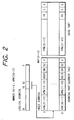
«Support of Plural Index Methods»
The data processor for supporting the virtual
memory comprises: a buffer memory including a set
associative type cache memory having a plurality of
banks which individually have memory fields for
storing the corresponding informations between virtual
page numbers and physical page numbers and which are
to be individually accessed by a shared index address;
and means for making variable a method of generating
index addresses for the buffer memories. For example,
in the case of a multiple virtual support in which
there are a plurality of processes individually having
address translation informations so that they are
discriminated by their numbers, either of the method
of decoding only a portion (i.e., the bits 12 to 16)
of the logical address, as exemplified in Fig. 2, or
the method of decoding the result which is obtained by
modifying (i.e., XOR = Exclusive OR) a portion (i.e.,
the bits 12 to 16) of the logical address by a portion
of the present process number (asid), as shown in Fig.
3, is indicated as the address designating method for
indexing the entry from the buffer memory in
accordance with the logical value of a register
MMUCR.IX. Incidentally, those informations of the
virtual page number VPN contained in the translation
pair in the buffer memory 1, which correspond to the
vpn (16 - 12) to be used for the index, are eliminated
and designated at VPN (31 - 17) and VPN (11 - 10) in
Figs. 3 and 2. Here, the designation of the vpn (16 -
12) implies the information of the virtual page number
containing, the bits 12 to 16 of the logical address.
The designation of the VPN (31 - 17) implies the
information of the virtual page number as the entries
of the buffer memory corresponding to the bits 17 to
31 of the logical address.
«Degree of Freedom of Replacement»
The data processor for supporting the virtual
memory comprises the buffer memory 1 including a 4-way
set associative type cache memory having the plural
banks 11 to 14 which individually have memory fields
for latching the corresponding informations between
the virtual page number VPN and the physical page
number PPN and which have their individual index
addresses shared. In case the latched information is
to be replaced from those plural banks due to
occurrence of a cache miss, the set to be replaced can
be arbitrarily designated by executing a software by
the central processing unit. For example, the
register MMUCR.RC is a register to be set with
information of 2 bits for designating the
aforementioned banks arbitrarily. When a value set in
this register is decoded by a decoder 17, signals BSL1
to BSL4 are generated for selecting one of the four
banks 11 to 14. As a result, one of the four banks 11
to 14, as designated by the selecting signals, that
is, one entry designated by the index address 2 is a
target of replacement. When the value for the bit
MMUCR.RC in that register MMUCR is set by the hardware
means, the bank designation by this hardware means can
be arbitrarily changed by executing the software by
the aforementioned central processing unit (CPU).
The aforementioned hardware means is equipped
with the register MMUCR.RC as counter means such as a
random counter, as shown in Fig. 4. This counter
means has the power of two of the bit number equalized
to the number (= 4) of the banks of the buffer memory
1. A control circuit CTRL contained in the
aforementioned hardware means increments the counter
means by one, in case the latched information is to be
replaced for the buffer memory 1, and sets the
incremented result to the bank number to be replaced,
in case valid data are also latched in the indexed
memory field of any bank (that is, in case each entry
of each of the indexed banks has a valid bit V
indicating the validity "1"). In case, on the other
hand, the valid data are not latched in the indexed
memory field (that is, in case each indexed entry has
the valid bit V indicating the invalidity "0"), the
control circuit CTRL sets the counter means with the
number of the bank including the entry latching no
valid data. According to this predetermined rule, the
bank to be replaced is designated. At this time, each
bit of the aforementioned counter means is a target to
be changed to an arbitrary value by the software which
is executed by the central processing unit.
«Support of Single Virtual Memory and Multiple Virtual
Memory»
The data processor for supporting the virtual
memory comprises an address translation mechanism for
dividing the logical address space into units called
the "virtual pages" thereby to translate the logical
address into the physical address at the page unit.
This address translation mechanism comprises: a
multiple virtual support for modifying or expanding
the logical address for the address space identifier
(asid), when each of the processes has an address
translation information covering all over the logical
space; and a single virtual support for neither
modifying nor expanding the logical address for the
address space identifier (asid) when a portion of the
logical address space is exclusively assigned to the
plural processes so that each process has the address
translation information of the logical address space
assigned thereto. The address translation mechanism
can select the multiple virtual support and the single
virtual support. As result, each entry in the buffer
memory is provided, as shown in Fig. 5, with not only
the translation pair of the virtual page number VPN
and the physical page number PPN but also the field of
the address space identifier ASID. This content of
this field is processed differently according to the
single virtual support or the multiple virtual
support. When the virtual page corresponding to the
address space identifier contained in a TLB entry
cannot be shared with another process, the content of
the field of the address space identifier ASID is used
in the multiple virtual support for deciding the
retrieval hit/miss (i.e., TLB hit / TLB miss) for the
buffer memory. In this case, the TLB hit is not
decided if the information of the virtual page number
VPN of the entry latched in the buffer memory matches
the information of the virtual page address vpn and if
the address space identifier ASID of the same entry
mismatches the present address space identifier asid.
In the single virtual support, the content of the
field of the address space identifier ASID is used as
the memory protecting information. In this case, when
the TLB miss occurs due to the difference in the
address space identifier, it is decided by the
software which of the difference in the address space
identifier or in the virtual page address the miss is
caused. In case the miss is caused by the difference
in the address space identifier, the miss is treated
as the protection error. Which of the aforementioned
single virtual support or multiple virtual support is
indicated by the value of the bit MMUCR.SV of the
register MMUCR, as shown in Fig. 6. The value of this
bit MMUCR.SV can be arbitrarily set by the software to
be executed by the central processing unit.
Thanks to the construction described above, the
following effects can be achieved.
The data processor for supporting the plural page
sizes selectively is easily enabled to satisfy the
demand for improving the using efficiency of the
memory by each process by making the size of the
virtual pages relatively small, in case the total
memory capacity of the real memory to be packaged in
the system is short. If, at this time, the maximum
virtual page size is set to the power of two of the
minimum size whereas the number of the banks of the
set associative type buffer memory is set to the power
of two of the same, the entries of the same number of
any virtual page number can be latched on principle in
the buffer memory independently of the size of the
virtual page to be selected, even if the method of
designating the index address is made identical to
that for the maximum virtual page size. If the bit
number of the address comparison to be reflected on
the hit decision is changed by using the information
for indicating size of the virtual page, the bit
number or position of the information to be compared
for retrieving the buffer memory associatively can be
changed according to the size of the virtual page. If
the buffer memory for supporting the plural page sizes
is realized by the set associative type cache memory,
both the chip occupation area and the power
consumption are reduced to halves as large as those of
the construction of the CAM.
According to the means for supporting the plural
index methods, these methods can be so selected
according to the using mode, in which many processes
are started in parallel in the multiple virtual
support, as to suppress the reduction of the hit rate
in the using mode. The reduction of the hit rate in
the using mode, in which many processes are started in
parallel in the multiple virtual support, can be
suppressed by modifying a portion of the logical
address with the address space identifier (asid) using
the same logical address thereby to index the buffer
memory.
According to the means for improving the degree
of freedom for the replacement, the bank to be
replaced can be arbitrarily decided by the software
without fixing the replacement algorithm for replacing
the translation pair of the buffer memory. As a
result, it is possible in the data processing
conveniences to satisfy the demand for latching a
specific translation pair as the entry in the
translation lookaside buffer at all times and the
demand for preventing the specific address translation
pair from being replaced. The provision of the
register for instructing the target of replacement by
the software can ensure the degree of freedom for the
replacement according to the random, FIFO and LRU
types in dependence upon the algorithm of the
software.
The means for the single virtual support and the
multiple virtual support can improve the using
conveniences of the address translation mechanism.
These using conveniences can be improved better by
selecting either of them through the software. If the
address space identifier (ASID) in the multiple
virtual support is used as the memory protecting
information in the single virtual support, it is
easily possible to complete the memory protection in
case the single virtual support is selected.
BRIEF DESCRIPTION OF THE DRAWINGS
Fig. 1 is an explanatory diagram of a
construction for supporting a plurality of page sizes
in a microcomputer according to one embodiment of the
present invention;
Fig. 2 is an explanatory diagram of a method of
indexing a TLB by using a portion of a virtual page
address as it is;
Fig. 3 is an explanatory diagram of a method of
indexing the TLB by using a portion of the virtual
page address and a portion of a address space
identifier;
Fig. 4 is an explanatory diagram of a construction
capable of deciding a bank, as is to be replaced,
of a TLB entry arbitrarily by a software;
Fig. 5 is an explanatory diagram for explaining
different logical addresses of a page size and
examples of the format of the TLB entry for supporting
them;
Fig. 6 is an explanatory diagram for explaining
examples of various registers for the TLB;
Fig. 7 is an overall block diagram showing an
essential portion of the microcomputer according to
one embodiment of the present invention;
Figs. 8(A) and 8(B) are explanatory diagrams for
explaining an address map to be supported by the
microcomputer of the present embodiment;
Fig. 9 is an explanatory diagram of an access
right to be regulated by a protection bit PR used for
memory protection;
Fig. 10 is a control main flow chart of an
address translation;
Fig. 11 is a control flow chart for selecting an
index method of the TLB;
Fig. 12 is a control flow chart for comparing the
logical address and the address of a tag indexed by
the former;
Fig. 13 is a flow chart of a portion of the
protection control containing the control for using an
ASID for the memory protection in a single virtual
support;
Fig. 14 is a flow chart showing a procedure of
generating a physical address according to a page
size;
Fig. 15 is a control flow chart for designating a
bank to be replaced, by a hardware;
Fig. 16 is a flow chart showing one example of
the processing of a TLB miss handler for updating the
TLB entry to be started by an exception caused by the
TLB miss;
Fig. 17 is a flow chart showing a first half of
the exception detecting process relating to the TLB in
the single virtual support;
Fig. 18 is a flow chart showing a second half of
the exception detecting process relating to the TLB in
the single virtual support;
Fig. 19 is an explanatory diagram showing the
overall differences between the single virtual support
and the multiple virtual support;
Figs. 20(A) and 20(B) are explanatory diagrams
showing the concepts of the single virtual support and
the multiple virtual support;
Fig. 21 is a logical circuit diagram showing one
example of the control logic for controlling the
address comparison result to be reflected upon a hit
signal in each bank of the TLB; and
Fig. 22 is a block diagram showing a portion of
Fig. 7 in more detail.
DESCRIPTION OF THE PREFERRED EMBODIMENTS
«Microcomputer»
Fig. 7 shows an essential portion of a
microcomputer according to one embodiment of the data
processor of the present invention. The microcomputer
of the present embodiment is formed over one
semiconductor substrate of single crystal silicon by
the well-known semiconductor integrated circuit
manufacturing technique, although not especially
limited thereto. In Fig. 7, there are shown as
representative circuit blocks a logical address bus
VABUS, a physical address bus PABUS, data bus DBUS, a
central processing unit (CPU) 3, a cache memory
(CACHE) 4, a translation lookaside buffer (TLB) 1 as
the buffer memory, and a TLB controller (TLBC) 5. The
CPU 3 fetches an instruction from a not-shown program
memory and processes the data in accordance with the
description of the instruction. In case an external
access is required, the CPU 3 outputs a logical
address to the logical address bus VABUS and inputs/
outputs the data through the data bus DBUS. The cache
memory 4 is exemplified by the 4-way set associative
type, although not especially limitative thereto. The
band is indexed by using a portion of the logical
address fed from the logical address bus VABUS. The
physical address is latched in the tag portion of the
entry. The tag portion thus indexed has its logical
address translated by the translation lookaside buffer
1 and is compared with the physical address outputted
to the physical address bus PABUS. The cache miss/hit
are decided according to the comparison result.
The microcomputer of the present embodiment
divides the logical address space into the units
called the "virtual page" and supports the virtual
memory for the address translation from the logical
address into the physical address at the page unit.
The aforementioned translation lookaside buffer 1
latches the translation pair between a virtual page
number VPN and a corresponding physical page number
PPN, as the TLB entry. The TLB controller 5
translates the logical address outputted from the
central processing unit 3 into the physical address by
using the translation lookaside buffer 1. This
translation lookaside buffer 1 is constructed of a
4-way set associative type cache memory having four
banks sharing the index addresses. Although only one
bank 11 is representatively shown in Fig. 7 so as to
avoid the complex illustrations, other banks 12 to 14
like the bank 11 are actually arranged in the
direction to and from the drawing, as shown in Fig. 1.
The address translation mechanism for the aforementioned
virtual support is constructed of the
aforementioned translation lookaside buffer 1, TLB
controller 5 and CPU 3 and the system software or
operating system for the address translation and the
memory protection.
Here will be described in advance the address
space of the microcomputer of the present embodiment.
In the microcomputer of the present embodiment, the
central processing unit 3 forms a logical address of
32 bits so as to support the logical address space of
4 GB. The logical address is made expandable by the
later-described address space identifier (or space
identifier) asid. In Figs. 8(A) and 8(B), there is
illustrated the address mapping of the logical address
space which is supported. In these Figures, the
fields, as "Mapped", are those to be subjected to the
address translation making use of the translation
lookaside buffer (TLB) 1. The fields H'FFFFFFFF
(wherein H' designates a hexadecimal notation) to
H'80000000 can be accessed in the privileged mode and
decided as the address error if accessed in the user
mode. A P4 field is a control space which is mapped
with a peripheral control register. P1 and P2 fields
are those, in which the corresponding physical
addresses are fixed, and are not subjected to the
address translation using the translation lookaside
buffer 1. These fields P1 and P2 have their logical
addresses translated into physical addresses by adding
or subtracting a predetermined constant. In the
privileged mode, therefore, no exception relating to
the address translation, as started from the TLB miss,
is made if the fields P1 and P2 are accessed.
Especially, the P2 field is not cached by the cache
memory CACHE, but the Pl field is not cached.
The microcomputer of the present embodiment has
the privileged mode and the user mode, as described
above, and it is indicated by the value of the mode
bit MD of a status register SR contained in the
central processing unit 3 whether the microcomputer is
operating in the privileged mode or the user mode.
The operation in the user mode is indicated by MD = 0,
and the operation in the privileged mode is indicated
by MD = 1. In the privileged status (as set in the
privileged mode), as shown in Fig. 8(A) and (B)it is
possible to access the address space (from P1 to P4)
which will cause the address error if accessed in the
user status (as set in the user mode) so that the
privileged instruction or system control instruction,
as cannot be executed in the user status, can be
executed, as different from the user status.
In the logical address space of 4 GB, as shown in
Figs. 8(A) and 8(B), the PO field and the P3 field are
plurally divided at the unit called the virtual page,
so that the logical address is translated into the
physical address at the unit of the divided pages,
although not especially limitative thereto. The
virtual pages to be supported by the microcomputer of
the present embodiment have two kinds of 4 KB and 1
KB. This satisfies the relation that the maximum size
(= 4 KB) of the virtual pages to be supported is set
to the power of two whereas the number (= 4) of the
banks of the translation lookaside buffer 1 is no less
than the power of two of the former. In case the
virtual page size is 1 KB, as shown in Fig. 5, in the
logical addresses (i.e., the addresses of 32 bits from
the bit 0 to the bit 31) to be generated by the
central processing unit, the bits 0 to 9 are offset
whereas the bits 10 to 31 are set to the virtual page
numbers (or the virtual page addresses). In case the
virtual page size is 4 KB, in the logical addresses,
the bits 0 to 11 are offset whereas the bits 12 to 31
are set to the virtual page numbers (or the virtual
page addresses). The index for the translation
lookaside buffer 1 is exemplified the information of
the bit positions of the less significant five bits of
the virtual page addresses of the page size of 4 KB,
that is, the bits 12 to 16 of the logical addresses of
32 bits no matter whether the page size might be 4 KB
or 1 KB. In the case of translation from the logical
address into the physical address, the physical
addresses are acquired by acquiring the physical page
number from the entry corresponding to the virtual
page number of the logical address and by adding the
offset information of the logical address to the less
significant side of the physical page number.
If a TLB miss occurs, the information (i.e., the
page table entry) to be fetched by the entry in the
translation lookaside buffer 1 is generated in advance
by the software and is latched in the external memory
(e.g., the memory RAM of Fig. 22) which is omitted
from Fig. 7. Specifically, the page table entry for
the virtual memory includes the description of the
translation information indicating the correspondence
between the virtual page number VPN and the physical
page number PPN or the attributes of the access and is
latched in the page table which is formed in the
external memory. For a fast address translation, the
entry latched in the page table is partially latched
in the banks 11 to 14 of the aforementioned TLB 1.
The addresses of the page table in the external memory
are set in advance in the translation table register
(TTB), as will be described with reference to Fig. 6.
If a TLB miss occurs, the base address set in the
translation tale register 53 and the virtual page
number at the time of the miss are used by the CPU 3
to access the aforementioned page table thereby to
determine the entry containing the physical page
number corresponding to the virtual page number at
that time. The entry thus determined is written to
the bank in the TLB 1, for example. As a result, the
physical address corresponding to the logical address
at that time is generated.
The entry to be latched in each bank of the TLB 1
is conveniently divided into an address part and a
data part, as shown in detail in Fig. 5. The address
part is composed of the informations VPN (31 - 17) and
VPN (11 - 10) of the virtual page number, a valid bit
V (of 1 bit) indicating the validity of the entry, a
space identifier ASID (of 8 bits), a size bit SZ (of 1
bit), and a share status SH (of 1 bit). The data part
is composed of a protection PR (of 2 bits) for memory
protection, the physical page number PPN (of 22 bits)
corresponding to the virtual page number, a dirty bit
D (of 1 bit), and a cacheable bit C (of 1 bit). The
informations of the virtual page numbers latched by
the address part are the bits 10 to 11 and the bits 17
to 31 of the logical addresses of 32 bits, from which
the bits to be used for indexing the bit format are
excluded. The former bits are expressed by the VPN
(11 - 10) whereas the latter bits are expressed by the
VPN (31 - 17). The share status SH indicates whether
or not the corresponding page is shared among the
plural processes, and the non-share status is
indicated by SH = 0 whereas the share status is
indicated by SH = 1. The space identifier ASID is
used as belongs to a specific process to define the
virtual page, and will also be called the "address
space identifier". The protection PR is the data
which are encoded to define the access right for the
page, and the access right is defined in the modes
shown in Fig. 9 by combining its values. The size bit
SZ is a bit for designating the virtual page size, and
the page size of 4 KB is designated by the logical
value 1 whereas the page size of 1 KB is designated by
the logical value 0.
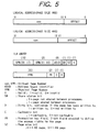
Here will be described the concepts of the single
virtual support and the multiple virtual support with
reference to Figs. 20(A) and 20(B). The multiple
virtual support is defined to modify or expand the
logical address by the address space identifier asid
when each of the plural processes has the address
translation information covering all over the logical
space. In the single-virtual support, on the
contrary, a portion of the logical address space is
exclusively assigned to the plural processes. In
other words, the single virtual support is defined to
neither modify nor expand the logical address by the
address space identifier asid when each process has
the address translation information of the logical
address spaced assigned thereto. Thus in the single
virtual support, the logical address space is
exclusively assigned among the plural processes so
that each logical address space assigned to the
process has its intrinsic address translation
information, as shown in Fig. 20(B). This allows only
one address translation table to exist. By using this
one address translation table, a certain logical
address A is uniquely translated into a corresponding
physical address D. In the multiple virtual support,
on the other hand, the logical address space is
assigned in a mutually overlapping manner among the
plural processes. Hence, the address translation
informations for the individual processes have to be
contained in the mutually different address
translation tables. As a result, the logical address
A is transformed into different physical addresses B
and C through mutually different address translation
tables i and j. At this time, it is discriminated by
the address space identifier which process the logical
address A to be translated belongs to. In the
multiple virtual support, according to Fig. 20(A), the
address translation table i corresponds to the address
space identifier i whereas the address translation
table j corresponds to the address space identifier j.
These address space identifiers can be deemed as the
discrimination numbers in the plural processes using
(or accessing) a mutually identical logical address
space. Fig. 19 illustrates the differences between
the single virtual support and the multiple virtual
support as to the logical space, the translation
information and the protection. In Fig. 19, letters
PR designate the protection information, as shown in
Fig. 9.
In Fig. 7, the aforementioned TLB controller 5
includes a controller (CTRL) 50, a page table entry
high (PTEH) register 51, a page table entry low (PTEL)
register 52, a translation table base (TTB) register
53, a TLB exception address (TEA) register 54, and a
control (MMUCR) register 55. These registers are
coupled to the CPU 3, as will be described with
reference to Fig. 22. Of these, at least the TEA
register 54 and the MMUCR register 55 can be directly
read/written by the CPU 3. The remaining registers 51
to 53 can also be accessed by the CPU 3.
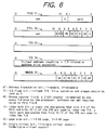
As shown in Fig. 6, the PTEH register 51 and the
PTEL register 52 are provided with the field which can
latch the page table entry for updating or adding the
entry of the TLB 1 at the time of a TLB miss. The
PTEH register 51 is set with the space identifier asid
of the present process from the central processing
unit 3 by executing the software. Moreover, the PTEH
register 51 is also given a function to latch the
virtual page address vpn of the TLB miss outputted by
the CPU 3, if the TLB miss occurs. The offset of the
logical address outputted from the CPU 3 is latched in
the not-shown latch circuit in the CTRL 50. The base
address of the present page table is latched in the
TTB register 53. The TEA register 54 latches the
logical address when an exception to the TLB or an
address error exception occurs. The MMUCR register 55
contains: a bit AT (which is valid for the logical
value 1 and invalid for the logical value 0)
instructing whether the address translation is to be
validated or invalidated; a bit TF instructing the
flushing of the TLB 1; a random counter field RC of 2
bits; an index mode bit IX for designating the index
mode; and a single virtual bit SV (for selecting the
single virtual support for SV = 1 and the multiple
virtual support for SV = 0) for instructing which of
the single virtual support or the multiple virtual
support is to be selected. In case the aforementioned
index mode bit IX is at 1, there is selected the index
method using the asid (4 - 0), i.e., the bits 0 to 4
of the present space identifier asid and the bits 12
to 16 of the virtual page number vpn being outputted
from the central processing unit 3, as shown in Fig.
3. In the case of IX = 0, on the contrary, there is
selected the index method using the bits 12 to 16 of
the virtual page number vpn being outputted from the
central processing unit 3, as shown in Fig. 2. More
specifically, the index address for the case of IX = 1
is generated by an exclusive OR gate XOR inputting the
bits 0 to 4 of the space identifier asid owned by the
PTEH register 51 and the bits 12 to 16 of the virtual
page number vpn being outputted from the CPU 3, i.e.,
the vpn (16 - 12), as shown in Fig. 7. A selector 18
of Fig. 7 selects either the output hashed by the
exclusive OR gate XOR or the vpn (16 - 12) as the
indexing address. The control for this selection is
determined according to the value of the index mode
bit IX by the select signal 550 outputted from the
CTRL 50.
Of the virtual page numbers vpn (31 - 10) of the
logical addresses outputted from the CPU 3, as shown
in Fig. 7, the vpn (16 - 12) corresponding to the bits
12 to 16 are used to generate the index address 2
shared among the four banks 11 to 14 in the TLB.
Since the virtual page number is expressed by 5 bits,
as described above, the thirty two entries of each
banks are selected and read out one by one by the
shared index address 2. Each of the entries to be
selected contains, as its information, the VPN (31 -
17), the VPN (11 - 10), the ASID, the SH, the SZ, the
V, the PPN (31 - 10), the PR, the C and the D. Of the
informations of the entries selected and read out: the
read VPN (31 - 17) are compared by a comparator 151
with the vpn (31 - 17) of the logical addresses
outputted from the central processing unit 3; the VPN
(11 - 10) are compared by a comparator 152 with the
vpn (11 - 10) of the logical addresses outputted from
the central processing unit 3; and the ASID read out
is compared by a comparator 153 with the present space
identifier asid latched by the PTEH register 51. For
the comparison results, a control logic 154 decides
the miss/hit of the bank 11 by considering the values
of the share status SH, the size bit SZ, the single
virtual bit SV and the mode bit MD. The hit signal
hitl is the decision result of the miss/hit in the
bank 11. The aforementioned comparators 151 to 153
and control logic 154 are provided for each of the
banks 11 to 14. In Fig. 7, the hit signals hit2 to
hit4 are representatively shown for the individual
banks 12 to 14. According to the present embodiment,
the outputs of the individual comparators 151 to 153
are given the matched high level. The high levels of
the hit signals hitl to hit4 are used as the hit
level. The control circuit 50 decides the TLB hit if
any of the hit signals hitl to hit4 is set to the hit
level. Reference numeral 501 appearing in Fig. 7
designates a TLB hit signal for informing the CPU 3 of
the decision result of the TLB hit/miss. When the TLB
miss occurs, the entry of the translation lookaside
buffer 1 is replaced. In this replacement, the
content of the entry to be replaced is latched in the
PTEH register 51 and the PTEL register 52 so that the
information to be replaced is fed from the PTEH
register 51 and the PTEL register 52 is fed to and
fetched in the TLB 1. The index method for selecting
the entry to be replaced is identical to that at the
aforementioned reading time, but which bank (or set)
that entry is to be latched is decided by the value
(MMUCR.RC) of the RC of the MMUCR register 55.
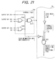
Fig. 21 shows one example of the logical
construction of the aforementioned control logic 154.
Numeral 1541 designates a three-input AND gate;
numeral 1542 a two-input OR gate; and numeral 1543 a
two-input OR gate. The OR gate 1542 inputs both the
output of the comparator 152 or the result of the
comparison between the VPN (11 - 10) contained in the
indexed TLB entry (i.e., the entry selected and read
out by the index address) and the vpn (11 - 10)
contained in the logical address and the size bit SZ
coming from the aforementioned indexed TLB entry. In
case the size bit SZ is set to 1 so that the virtual
page size of 4 KB is indicated, there is no need for
comparing the VPN (11 - 10) in the TLB entry and the
vpn (11 - 10) from the CPU 3, in the address
comparison for deciding the TLB miss/hit. In the
status of the size bit SZ = 1, therefore, the
comparison result of the aforementioned address bits
11 and 10 is not reflected upon the output signal hitl
of the AND gate 1541. In case the size bit SZ is set
to O to indicate the virtual page size of 1 KB, the
comparison between the address bits 11 and 10 is
required for the decision of the TLB miss/hit, and the
comparison result is reflected upon the signal hit1.
The aforementioned OR gate 1543 inputs both the
output of the comparator 153 or the result of
comparison between the address space identifier ASID
contained in the indexed TLB entry and the present
address space identifier (or the address space
identifier outputted from the PTEH register 51) asid
and the shared bit SH coming from the aforementioned
indexed TLB entry. In case this shared bit SH is at
1, the status of "sharing the virtual page among the
processes" is indicated. In this status, therefore,
the comparison between the address space identifiers
is not required in the address comparison for the
decision of the TLB miss/hit. In the status of the
shared bit SH = 1, therefore, the comparison result
between the address space identifiers is not reflected
upon the output signal hitl of the AND gate 1541. In
case the shared bit SH in the aforementioned index is
set to 0 to instruct the "non-share status of the
virtual page among the processes", the comparison
between the address space identifiers is required in
the address comparison for the decision of the TLB
miss/hit. In the status of the shared bit SH = 0,
therefore, the comparison result between the address
space identifiers is reflected upon the output signal
hitl of the AND gate 1541.
In the single virtual support, the aforementioned
address space identifier ASID owned by the TLB entry
is used as the memory protecting information (or
domain number). In not only the single virtual
support but also the multiple virtual support, the
share or non-share status is indicated by the shared
bit SH. When the non-share is indicated, the mismatch
between the present address space identifier asid and
the address space identifier ASID contained in the TLB
entry is decided as the TLB miss in the multiple
virtual support. When the non-share is indicated, on
the contrary, the mismatch between the address space
identifiers asid and ASID is used in the single
virtual support for detecting the TLB protection error
exception. In order to realize this, the control
circuit 50 is equipped with an AND gate 502, as shown
in Fig. 21, as one logic for checking the access
right. In response to the inverted output of the
aforementioned OR gate 1543, the signal virtual bit SV
from the MMUCR register and the inverted signal of the
mode bit MD in the status register in the central
processing unit 3, the AND gate 502 generates a TLB
protection error exception detection signal 503. This
detection signal 503 has its high level at the
detection level of the TLB protection error exception.
This TLB protection error exception is detected by the
signal 503 only when the address space identifiers
mismatch and are not shared (that is, when the output
of the OR gate 1543 is at the low level) and when the
conditions for the single virtual support (SV = 1) and
the user mode (MD = 0). Specifically, if the address
space identifiers mismatch and are not shared in the
single virtual support, the TLB miss is substantially
decided. This status is set to the TLB protection
error exception for the memory protection. In the
privileges status indicated by the mode bit MD = 1, it
is desired that the virtual page assigned to another
process can also be accessed. In the privileged
status of MD = 1, therefore, the TLB protection error
exception is not detected.
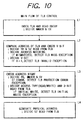
Fig. 10 is a main flow chart showing the control
of an address translation by the control circuit 50.
This control is coarsely divided into a step L1 of
indexing the translation lookaside buffer 1, a step L2
of comparing the addresses and checking the V-bit, a
step L3 of checking the access right, and a step L4 of
generating the physical address. These steps are
controlled by the CPU 3 and the controller 5.
At the step L1 of indexing the translation
lookaside buffer 1, the logical address to be used in
this step is set to vpn (16 - 12) irrespective of its
size. At this index step, it is decided by the value
(MMUCR.IX) of the IX of the MMUCR register 55 whether
or not the logical address hashed by the portion asid
(4 - 0) of the space identifier asid is to be used as
the indexing address by the exclusive OR gate XOR. In
case the MMUCR.IX is at 1, as shown in Fig. 11, the
aforementioned used logical address is hashed to the
indexing address by the asid (4 - 0). In case the
MMUCR.IX is at 0, on the other hand, the vpn (16 - 12)
is used as it is as the indexing address. The former
index method is shown in Fig. 3 whereas the latter
index method is shown in Fig. 2. When the TLB 1 is
indexed, one of the thirty two entries is selected and
read out from each of the banks 11 to 14. Each entry
to be selected contains the VPN (31 - 12), the VPN (11
- 10), the ASID, the SH, the SZ, the V, the PPN (31 -
10), the PR, the C and the D as its information.
In Fig. 12, there is shown on example of the
procedure of the address comparison to be executed at
the step L2 of comparing the addresses and checking
the V-bit. The procedure, as shown herein, is based
upon the logic of the control logic 154 shown in Fig.
21, but the detection of the TLB protection error
exception is also considered as to the comparison of
the space identifier ASID. How to determine the
object of the address comparison to be reflected upon
the hit signals hit1 to hit4 is decided, as follows.
First of all, whether or not the space identifier is
considered as the object of the address comparison is
coarsely decided depending upon whether or not the SH
is at 1. Whether or not the VPN (11 - 10) is
considered as the object of the address comparison is
decided depending upon whether or not the SZ is at 0.
Especially in the single virtual support (SV = 1), the
infield data of the space identifier ASID are used as
the memory protection information. In the single
virtual support and in the privileged mode (SV = 1 and
MD = 1), however, the field of the space identifier
ASID is excluded from the comparison object so that
the virtual page assigned in the privileged mode to
another process may also be accessed from the present
process, that is, so that the TLB protection error
exception may not be detected.
By this index, the TLB entry is read from the TLB
1. On the basis of the share status SH in the read
TLB entry, it is decided whether or not the space
identifier ASID is to be considered at the time of the
address comparison. The space identifier ASID is not
considered as the object of the address comparison in
the case of SH = 1 (share) but is considered as the
object of the address comparison in the case of the SH
= 0 (non-share). Moreover, in case the value
(MMUCR.SV) of the SV of the MMUCR register 55 is set
to 1 so that the single virtual support is set and in
case the mode bit SR.MD of the status register SR is
at 1 (that is, the central processing unit is
operating in the privileged mode), the space
identifier ASID is not considered in the detection of
the TLB protection error exception. This is intended
from the characteristics of the privileged mode to
make it possible to access the virtual page assigned
to another process from the present process.
In the present embodiment, the size of 1 KB or 4
KB is selected as the size of the virtual page in
accordance with the value of the size bit SZ in the
TLB entry. In case the size of the virtual page is at
1 KB, the informations VPN (31 - 17) and VPN (11 - 10)
in the TLB entry, as indexed in each bank, are made
the objects of comparison with the corresponding bits
vpn (31 - 17) and vpn (11 - 10) of the logical
address. In case the virtual page size is at 4 KB,
the VPN (11 - 10) in the TLB entry, as indexed in each
bank, and the corresponding vpn (11 - 10) in the
virtual page are excluded from the object of the
comparison decision.
As described above, the comparison objects (VPN
(31 - 17, 11 - 10), vpn (31 - 17, 11 - 10), ASID and
asid) are determined and compared. If a matching
occurs in any bank as a result of the comparisons, a
hit signal is outputted from the matching bank. The
hits of the individual banks are outputted as the hit
signals hitl to hit4 so that the TLB hit is decided.
If no hit signal is outputted from all the banks, that
is, in the mismatching case, on the contrary, the TLB
miss exception is detected. This result is informed
by the signal 501 to the CPU 3, which processes the
TLB miss exception, as will be described hereinafter.
For the entry of each indexed bank, moreover, the
V-bit in the entry is checked. In other words, the
V-bit in the read entry is checked. In the case of
the TLB hit, if the V-bit in the hit entry is 0
(invalid), the TLB invalid exception is detected and
informed to the CPU 3. The content of this exception
processing will be described hereinafter. The
decision result of the V-bit in the case of the TLB
miss is used in the later-described entry replacement
relating to the TLB miss.
At the step L3 of checking the access right, the
access right is checked according to the content of
the information PR in the TLB entry read by the index
and the content of the bit MMUCR.SV in the MMUCR
register. As shown in Fig. 13, for example, it is
decided at first whether the bit MMUCR.SV in the MMUCR
register is at 1 (single virtual support) or 0
(multiple virtual support). In the case of the
multiple virtual support (SV = 0), the address space
expressed by the information in the TLB entry is
protected according to the content of the PR, as shown
in Fig. 9. In the case of the single virtual support
and the privileged mode, that is, in the case of
MMUCR.SV = 1 (single virtual support) and in case the
bit SR.MD = 1 (privileged mode) in the status
register, the address space, as expressed by the
information in the TLB entry, can be unconditionally
accessed. In the case of the user mode (SR.MD = 0:
user mode) despite the single virtual support, on the
contrary, the space identifier ASID and the share
status SH are considered at the time of checking the
access right. Specifically, either in case a matching
is satisfied between the space identifier asid of the
PTEH register 51 at the access time and the space
identifier ASID read from the TLB 1 or in the case of
SH = 1 (share), the address space, as expressed by the
information in the TLB entry, is protected according
to the aforementioned PR. In case the address space
identifiers are mismatched and non-shared, on the
contrary, the TLB protection error exception is
detected. The content of this exception will be
described hereinafter. At the access right checking
step L3, moreover, the access type is decided on
whether the access is for the reading or writing
operation, and the D-bit of the entry read from the
TLB 1 is decided. In case the access is at the first
write (i.e., the first write access after the power ON
or the reset), the TLB initial page write exception is
detected. Specifically, the TLB initial page write
exception is detected under the conditions that the
result of comparison between the logical address and
the indexed TLB entry is the TLB hit, that the dirty
bit D in the TLB entry is at 0 and that the access at
this time is a write access. The content of this TLB
initial page write exception processing will be
described hereinafter.
At the step L4 of generating the physical
address, the physical address is generated, as shown
in Fig. 14, in accordance with the size bit SZ of the
indexed TLB entry. The offset va (9-0) of a logical
address va to be used for generating a physical
address pa is latched in the latch circuit in the
control circuit CTRL 50, although not shown. If SA =
0 (the virtual page size is at 1 KB), the va (9 - 0)
of the logical address va outputted from the CPU 3 is
used as the offset pa (9 - 0) of the physical address
pa. Specifically, all the bits PPN (31 - 10) of the
physical page number PPN, as contained in the data
part of the hit TLB entry, is used the physical page
address pa (31 - 10). The address (9 - 0) is added as
the offset to the less significant side to generate
the physical address pa. If SZ = 1 (the virtual page
size is at 4 KB), the offset va (11 - 0) of the
logical address va outputted from the CPU 3 is used as
the offset pa (11 - 0) of the physical address pa. Of
the physical page number PPN contained in the data
part in the hit TLB entry, the PPN (31 - 12) having
its less significant 2 bits ignored is used as the
physical page address pa (31 -12). The address (11 -
0) is added as the offset to the less significant side
to generate the physical address pa.
Fig. 15 shows a hardware designation method of a
bank to be replaced in the TLB miss exception, as
detected at the step L2 of checking the address
comparison and the V-bit. This control is uniquely
executed by the control circuit 50 in accordance with
its logical construction and uses the bit MMUCR.RC of
the MMUCR register as counter means such as a random
counter. Here, the power of 2 of the bit number of
the MMUCR.RC is equalized to the number (= 4) of the
banks of the aforementioned TLB 1. In response to the
fact that none of the aforementioned hit signals hit1
to hit4 indicates the hit status, the control circuit
50 decides the necessity for the replacement of the
entry for the TLB 1. After this decision, the control
circuit 50 increments the MMUCR.RC by one (+1) to
examine whether or not an invalid entry is in the four
entries indexed. This is achieved by examining the
V-bit in each of the four indexed entries. In case
this examination of the V-bit reveals no invalid entry
(all the entries of each indexed bank latch the valid
data "V = 1"), the incremented result is used as the
bank number to be replaced and sets the MMUCR.RC to no
operation. In case an invalid entry is present (any
of the entries indexed in each bank exhibits V = 0 and
has no valid data latched), the bank number of the
bank having the invalid entry is set in the MMUCR.RC,
and the bank having the set number is used as the bank
to be replaced. Moreover, each bit of the
aforementioned MMUCR.RC can have its value arbitrarily
changed if the software is executed by the CPU 3. As
a result, the bank number set in this register, as
described above, can be further changed by the
software. As a result, any bank can be made the
object of replacement.
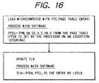
Fig. 16 shows a processing procedure by the TLB
miss handler for updating the TLB entry so as to cope
with the aforementioned TLB miss exception. A load
TLB instruction is used for updating the entry of the
TLB 1. This load TLB instruction (as will also be
expressed by the "LDTLB") is executed for the
following processing by the CPU 3. Specifically, the
values of the individual PTEH and PTEL registers 51
and 52 are written in the entries of the TLB 1. In
this case, the entries to be written are those in the
banks, which are indicated by the bank numbers set in
the MMUCR.RC, although not especially limitative
thereto, and are entries for indicating the logical
addresses (i.e., bits 12 to 16) latched in the PTEH
register 51, as the index addresses. If the
aforementioned TLB miss exception is detected, the
portion (i.e., the bits 10 to 31) of the logical
addresses at that time, as outputted from the CPU 3,
are latched in the aforementioned PTEH register 51.
As a result, the entry at the replacement time is
indicated by the index address of the same number as
that of the index address at the time which the TLB
miss exception occurs. However, the bank to be used
for the replacement is decided by the bank number
which is set in the MMUCR.RC.
In order to cope with the TLB miss exception, a
page table is prepared in advance by the user in the
external memory RAM, as shown in Fig. 22. In this
page table, a plurality of translation informations
(e.g., page table entries) corresponding to the
individual logical addresses are latched according to
predetermined rules, although not especially
limitative thereto. The addresses of this page table
such as a start address is latched in advance as the
base address in the register TTB 53. In this page
table, a plurality of page table entries individually
corresponding to the logical addresses are arranged
according to such rules as can retrieve the page table
entries (containing the corresponding physical page
number ppn, valid bit v, protection bit pr size bit
sz, cacheable bit c, dirty bit d and status sh)
corresponding to those logical addresses on the basis
of the aforementioned base addresses and logical
addresses as the start address, although not
especially limitative thereto.
The aforementioned TLB miss handler is described
by the user. This TLB miss handler is started by the
TLB miss handler when the TLB miss exception is
detected. As a result, the information vpn (10 - 31)
of the logical address upon the occurrence of the TLB
miss is latched in the PTEH register 51. At this
time, the space identifier asid at the occurrence of
the TLB miss may also be latched in the PTEH register
51. On the other hand, the CPU 3 retrieves the
aforementioned base table on the external memory by
using the base address latched in the register TTB 53
and the logical address at the occurrence of the TLB
miss. The page table entry corresponding to the
logical address at the occurrence of the TLB miss has
its content loaded, if discovered by that retrieval,
in the PTEL register 52. Next, the load TLB
instruction is issued so that the entries of the TLB 1
are updated by the values of the individual registers
PTEH and PTEL 51 and 52. As a result, the
informations vpn and asid of the logical addresses at
the occurrence of the TLB miss, as latched in the PTEH
register 51, are adopted as the partial VPN and ASID
of the TLB entries. Moreover, the entries to be
replaced at this time are those in the bank which is
indicated by the bank number set in the MMUCR.RC, as
described above, and are indicated by the same index
address as that at the occurrence of the TLB miss.
The aforementioned TLB invalid exception occurs
in the case of the page fault in the TLB hit. For
this exception, for example, the page table entry on
the external memory is recovered to set the V-bit in
the page table entry to the logical value 1. After
this, the PTEL register 52 is located with that page
table entry from the external memory, and the
aforementioned load TLB instruction is issued to up
data the corresponding entry of the TLB 1 by the
values of the individual PTEH and PTEL registers 51
and 52.
When the aforementioned TLB initial page write
exception is detected, the D-bit of the corresponding
page table entry on the external memory is set to the
logical value 1 to load the PTEL register 52 with that
page table entry from the external memory. After
this, the aforementioned load TLB instruction is
issued to update the corresponding entry of the TLB 1
by the values of the individual PTEH and PTEL
registers 51 and 52. Incidentally, the informations
vpn and asid of the logical addresses for causing the
exception are latched in the PTEH register 51. The
situation for the D = 1 is established at the first
write of the physical page field on the main memory.
In the virtual support, in order to match the data
between the auxiliary memory and the main memory
(e.g., the external memory of Fig. 22) at the page
replacement, it is necessary to decide whether or not
the content of the page of the main memory to be
replaced is to be copied back to the auxiliary memory.
The dirty bit D is used for this decision.
When the aforementioned TLB protection error
exception is detected, the virtual page number vpn of
the logical address for causing the exception is
written to the PTEH register 51, and the logical
address is written to the TEA register 54. After
this, the handler for solving that protection error is
started.
In case the MMUCR.RC is used as the counter, as
described above, the increment is desired for
registering a new bank entry at the time when the
aforementioned TLB miss exception is to be coped with.
For coping with the aforementioned invalid exception,
TLB initial page write exception and TLB protection
error exception, on the contrary, it is desired not to
increment the MMUCR.RC. This is because, in these
counter-measures, only the D-bit or V-bit is necessary
to change so that the TLB can be used more effectively
by no registration in a new bank than by a
registration in the original bank, although the
present invention should not be limited thereto.
Figs. 17 and 18 show the entirety of the
exception detecting flow of the TLB 1 in case the
multiple virtual support is indicated by setting the
bit MMUCR.SV of the MMUCR register to 0. According to
Fig. 17, the TLB 1 is indexed (at S1) by a
predetermined method according to the vpn of the
logical address and the present space identifier asid.
In case the indexed entry resultantly contains SH = 0
(non-share), the TLB miss exception (EX1) is detected
if the ASID or VPN mismatches (at S3). In case the
indexed entry contains SH = 1 (share), the ASID is not
compared, and the TLB miss exception (EX1) is detected
if the VPN mismatches (at S4). In the case of the TLB
hit (in case the answers of S3 and S4 are YES), it is
decided (at S5) whether or not V = 1. In the case of
V = 0 (invalid), the TLB invalid exception (EX2) is
detected. In the case of V = 1 (valid), it is decided
(at S6) from the bit SR.MD of the status register, as
shown in Fig. 18, whether the mode is the user mode
(User) or the privileged mode (Privileged). In case
(PR = 00 or 01) the CPU 3 is operating in the user
mode so that the entry read by the access by the CPU 3
operating in that mode has the information PR
indicating the allowance of the access in the
privileged mode (or the inhibition of the access in
the user mode), the TLB protection error exception
(EX3) is detected. In case, on the other hand, the
information PR in the read entry is decided to be at
10 by the access in the user mode, it is further
decided whether the access belongs to the read access
type or the write access type. If the information is
at 10, as shown in Fig. 9, the user access is allowed
to have only the read access type. In case,
therefore, the aforementioned access belongs to the
write access type, the access type is different (i.e.,
the write of S 7), the TLB protection error exception
(EX3) is detected.
In the case of PR = 00 or 10 even in the access
in the privileged mode, the TLB protection error
exception (EX4) is detected if the read/write access
type is contrary to the content of the PR (i.e., the
write of S8). Specifically, the access right to be
allowed by the PR is different depending upon whether
the CPU 3 is operating in the user mode or the in the
privileged mode. In either event, in case the access
is made in an access type other than that allowed by
the PR, the TLB protection error exceptions (EX3 and
EX4) are detected. In case the access type belongs to
the right (i.e., the write of S9 and S10) allowed by
the PR, the TLB initial write exception (EX5) is
detected if the information D in the entry is at 0 (or
unwritten page). In case the information D in the
entry is at 1, on the other hand, the cache memory 4
is accessed if the information C in the entry is at 1,
and the main memory (e.g., the external memory RAM or
ROM of Fig. 2) is accessed if C = 0. In case the
access type is the read (i.e., the read of S7 to S10)
allowed by the PR, the cache memory 4 is accessed if C
= 1, and the main memory is accessed if C = 0.
Fig. 22 mainly shows the connection relations
between the individual registers and the central
processing unit CPU, as shown in Fig. 7. The logical
addresses generated by the central processing unit CPU
are fed through the internal logical address bus VABUS
to the selector in the TLB control circuit TLBC. This
selector decodes the logical addresses and generates a
selection signal for selecting the registers in case
these logical addresses are intrinsic ones assigned to
the registers. In case the logical addresses are
those assigned to the PTEL register, for example, the
selector generates the selection signal C4 to select
that register. Likewise, the remaining registers
(PTEH, MMUCR, TEA and TTB) are selected. In other
words, these registers are address-mapped. The read/
write of the selected register by the central
processing unit are instructed through the not-shown
internal control bus by the read/write control signals
fed from the central processing unit to the individual
registers. It is quite natural that the individual
registers and the central processing unit CPU are
connected to each other through the internal data bus
DBUS, as shown. The individual registers are
connected with both the control circuit 51 and the TLB
1, as shown in Fig. 7, but are not so shown in Fig. 22
so as to avoid the complicated illustration. The
central processing unit is enabled to write the data
in the registers by executing the software.
Specifically, the central processing unit is enabled
to write the data in the registers by executing the
software to output the logical addresses assigned to
the registers to the bus VABUS, to output the data to
the bus DBUS and instruct the write by the read/write
signals. BY executing the software, the central
processing unit can also read out the data from the
registers. By thus executing the software, it is
possible to write the logical space identifiers and
the logical addresses at the TLB miss time in the PTEH
register, to write the table entry at the replacing
time in the PTEL register, to write the base address
in the TTB register, and to write the logical
addresses in the TEA register at the time of the
protection error exception. Moreover, the various
control data shown in Fig. 6 can be written in the
MMUCR register so that the specific bits can be used
as the counter.
The internal logical address bus VABUS is also
connected with the control circuit CTRL and the TLB 1.
The control circuit CTRL is equipped with a latch
circuit for latching the offset of the logical
address, as described above, so that the offset of the
logical address from the internal logical address bus
VABUS is latched. Moreover, the logical address from
the CPU 3 is fed to the TLB 1 through that internal
logical address bus VABUS so that it is used as the
index address and the retrieving address. It is quite
natural that the aforementioned latch circuit disposed
in the control circuit CTRL may latch not only the
offset address but all the logical addresses.
This drawing explicitly illustrates only the
connection between the aforementioned PTEH register
and TLB 1. The space identifier for deciding the
miss/hit of the TLB 1 is set in this register and fed
therefrom to the aforementioned TLB 1. In the
counter-measures for the miss exception of the TLB 1,
too, the logical addresses are fed from that register
to the TLB 1.
The internal data bus DBUS and the internal
physical address bus PABUS are connected with the
external data bus DBUS and the external address bus
ABUS through the external terminals TD and TA provided
in this data processor. With these external buses,
there are connected the external memories RAM and ROM,
as shown. Of these, the external memory RAM is a
volatile memory which is formed with the aforementioned
various tables, although not especially
limitative thereto. On the other hand, the external
memory ROM is a non-volatile memory which latches the
various programs (e.g., the software for the
aforementioned handler).
The effects and features of the virtual memories
in the microcomputer of the present embodiment will be
individually described in the following.
«Support of Plural Page Sizes»
As shown in Figs. 5 and 6, the page table entry
and the TLB entry have the aforementioned size bit SZ
so that the sizes of the virtual page can be set for
each page. The 4-way set associative type translation
lookaside buffer 1 is shared among the plural virtual
pages capable of having their sizes set variable. In
the present embodiment, two kinds of virtual page
sizes of 1 KB and 4 KB are supported by the microcomputer.
Moreover, the method of designating the
indexing addresses for the TLB 1 are made common
between 4 KB and 1 KB. In the present embodiment, as
shown in Figs. 2 and 3, of all the logical addresses
of 32 bits to be generated in the central processing
unit, the bits 12 to 16, i.e., the vpn (16 - 12) are
used for indexing the TLB 1. Since the index
addresses are of 5 bits, the maximum thirty two
entries can be retained for one bank (or way). Since
the TLB 1 has the four banks 11 to 14, the maximum
four entries can be retained for one index address.
In case the page size has 4 KB, the index addresses
are made to fall at the five bits vpn (16 - 12) from
the least significant one of the virtual page number
vpn. For the page size of 4 KB, the entries of an
arbitrary virtual page numbers can be retained at the
thirty two entries for each bank (i.e., one hundred
and twenty eight entries for all the banks). In the
case of the page size of 1 KB, on the other hand, the
vpn (11 - 10) of 2 bits from the least significant bit
of the virtual page number vpn is not used for the
indexing. If, therefore, the index of the case of one
bank is considered for the virtual page size of 1 KB,
the indexed entry indicates any of the four virtual
page numbers (each having a page size of 1 KB), as
selected by the index addresses of 5 bits. The 2 bits
(i.e., bits 10 and 11), as not used for the indexing,
are used to indicate any of the four virtual page
numbers selected. In case, therefore, only one bank
is present, only one entry is assigned to the four
consecutive virtual pages. In the present embodiment,
the maximum size of the virtual page is set to the
N-th power of two of the minimum size, and the number
of banks to be provided is also the N-th power of two.
Specifically, the virtual page has its minimum size
set to 1 KB and its maximum size set to the second
power of two of the former, i.e., 4 KB, and the number
of banks to be provided is the second power of two,
i.e., four. Thus, as in the case of the page size of
4 KB, the translation lookaside buffer 1 can latch one
hundred and twenty eight entries of an arbitrary
virtual page number, as has the page size of 1 KB as a
whole. However, the virtual page numbers of the
entries to be retained in one bank is restricted to
every 4 KB. This restriction exerts no influence upon
the hit rate of the TLB 1 if the virtual page numbers
of the entries retained by the translation lookaside
buffer 1 are consecutive. This hit rate is influenced
to some extent if the virtual page numbers are
discrete. In this case, too, the influence can be
reduced, if the virtual page of 1 KB is address-mapped
for every 2 KB, and can be fully eliminated if
address-mapped for every 4 KB. When the translation
information having the page size of 1 KB is to be set
in (or written to) the translation lookaside buffer 1,
the four entries (E11), (E12), (E13) and (E14), as
indicated by the index addresses of 5 bits, are set,
from the four banks (11), (12), (13) and (14),
respectively, with the translation information when
the 2-bit vpn (11 - 10) is at "00", the translation
information when the 2-bit vpn (11 - 10) is at "01",
the translation information when the 2-bit vpn (11 -
10) is at "10", and the translation information when
the 2-bit vpn (11 - 10) is at "11". Thus, it is
possible to prevent the reduction of the hit rate.
The bit number of the address comparison for the
hit decisions has to be changed according to the
virtual page size, as described with reference to Fig.
12. In case the virtual page is at 1 KB, the vpn (11
- 10) has to be compared with the VPN (11 - 10) unlike
the case of 4 KB. In order to cover all of such bit
numbers of comparison targets, the TLB 1 is provided
with the memory fields of the VPN (31 - 17) and the
VPN (11 - 10) and with the memory field of 22 bits
even for the physical page number PPN. The TLB 1 is
also provided in the data part of each entry with the
size bit SZ indicating the virtual page size to be
supported thereby, so that the bit number for the
address comparison for the bit decision is changed
according to the value of the size bit. In the case
of the size bit SZ = 1 (i.e., the virtual page size =
4 KB), as described with reference to Fig. 12, the VPN
(31 - 17) are compared with the corresponding bits of
the logical address. In the case of the size bit SZ =
0 (i.e., the virtual page size = 1 KB), the VPN (31 -
17) and the VPN (11 - 10) are compared with the
corresponding bits of the logical address.
Thus, the microcomputer for supporting the plural
page sizes selectively can easily satisfy the demand
for improving the memory using efficiency for each
process by making the sizes of the virtual pages
relatively small, in case the total memory capacity of
the real memory to be packaged in the system is small.
At this time, the translation lookaside buffer 1 is
enabled, by setting the maximum virtual page size to
the power of two of the minimum size and by the number
of banks of the set associative type TLB 1 to no less
than the power of two, to latch the entries of any
virtual page number on principle, even if the method
of indexing the index address is unified into that for
the maximum virtual page size and no matter whether
the selected virtual page size might be the maximum or
the minimum. If the information for indicating the
size of the virtual page is provided to correspond to
the virtual page number so that the bit number of the
address comparison for the hit decision is changed by
using that size, the number and position of the
comparison target information for retrieving the
translation lookaside buffer 1 associatively can be
easily changed according to the size of the virtual
page. If the translation lookaside buffer 1 for
supporting the plural page sizes is realized by the
set associative type cache memory, the chip occupation
area and the power consumption can be reduced to
halves of those of the case in which the same is
constructed of the CAM.
«Support of Plural Index Methods»
In case there is supported a multiple virtual
support in which a plurality of processes each having
address translation informations so that the processes
are discriminated by the address space identifier
asid, the method of decoding only one portion (i.e.,
the index addresses) of the logical addresses, as
shown in Fig. 2, and the method of decoding the result
of modifying one portion (i.e, the index addresses) of
the logical addresses with one portion of the present
address space identifier asid by the exclusive OR gate
XOR, as shown in Fig. 3, can be instructed as the
method of designating the index addresses of the TLB 1
in accordance with the logical values of the bit
MMUCR.IX of the register MMUCR. Thus, in the using
mode in which many processes are started in parallel
in the multiple virtual support, the index methods can
be so selected according to the using mode as to
suppress the reduction of the hit rate. If, moreover,
one portion of the logical addresses is modified by
the address space identifier asid using the logical
addresses to index the buffer memory, the reduction of
the hit rate can be suppressed in the using mode in
which many processes are started in parallel in the
multiple virtual support.
«Degree of Freedom of Replacement»
As described above, the TLB 1 is constructed as
the 4-way set associative type cache memory which is
provided with the plural banks 11 to 14 having their
index addresses shared. In case the latched
information is to be replaced from the plural banks
(or ways) due to a cache miss, the bank to be replaced
can be arbitrarily designated by executing the
software by the central processing unit 3. In the
register MMUCR shown in Fig. 6, the bit MMUCR.RC is a
field to be set with the information of 2 bits for
designating the aforementioned bank arbitrarily. This
set value is decoded by a decoder 17 of Fig. 4 to
generate signals (BSL1 to BSL4) for selecting one of
the four banks 11 to 14. As a result, one of the
entries in the four banks 11 to 14 designated by the
index address 2 is selected by the aforementioned
selection signals (BSL1 to BSL4) and is replaced. The
bit MMUCR.RC can also be used as the counter means
such as a random counter. The power of two of the bit
number of the MMUCR.RC is equalized to the number (4)
of the banks of the aforementioned buffer memory 1.
The control circuit (CTRL) 50 designates the banks in
accordance with the following predetermined rules, as
has been described with reference to Fig. 15. In case
the replacement of the latched information for the TLB
1 is required (for a TLB miss), the MMUCR.RC is
incremented by one. If any bank latches the effective
data in its indexed memory field (that is, the
translation information V in each of the index entries
latches the value 1), the incremented result is
adopted as the bank number to be replaced. In case
there is a bank having no effective data latched in
its indexed memory field (that is, some of the indexed
entries latches V = 0), the bank number is set in the
MMUCR.RC, and the bank having the set number is to be
replaced. At this time, the individual bits of the
MMUCR.RC are to have their values arbitrarily changed
by the execution of the software by the central
processing unit 3. Specifically, the MMUCR.RC is not
restricted to the increment of +1 due to the
occurrence of the TLB miss. The MMUCR.RC may be
updated to exclude a specific value. Moreover,
various replacements can be achieved depending upon
the algorithm of the software to be executed by the
CPU 3. For example, the random replacement, the FIFO
replacement starting from the initially loaded one,
and the LRU (Least Recently Used) replacement starting
from the last referred one can be easily realized by
changing the method of updating the MMUCR.RC. As a
result, it is possible to warrant the degree of
freedom of the replacement.
By not fixing these replacement algorithms for
replacing the entries of the TLB 1 but making it
possible to arbitrarily determine the banks to be
replaced, it is possible for the data processing
conveniences to satisfy the demand for latching a
specific translation pair at all times as the entries
in the translation lookaside buffer 1 and the demand
for leaving a specific entry unreplaced.
«Single Virtual Support and Multiple Virtual Support»
In the microcomputer of the present embodiment,
it is possible to select the multiple virtual support,
in which the logical address is modified or expanded
by the address space identifier asid, in case the
plural processes to be executed individually have the
address translation information all over the logical
space, and the single virtual support, in which the
logical address is neither modified nor expanded by
the address space identifier asid in case the
individual processes have the address translation
information of the logical address space assigned
thereto. The control of those virtual supports is
instructed by the value of the MMUCR.SV, as
exemplified in Fig. 6. The value of this MMUCR.SV is
arbitrarily set by the execution of the software by
the central processing unit 3. The conceptional
differences between the single virtual support and the
multiple virtual support have been described with
reference to Fig. 20, and the remaining representative
difference is exemplified in Fig. 19. As shown on
Fig. 5, the TLB 1 is provided with the fields for not
only the virtual page number VPN, the physical page
number PPN and the address space identifier ASID.
These fields have different values in dependence upon
whether the virtual support is single or multiple.
When the virtual page corresponding to the address
space identifier contained in a TLB entry is set not
to be shared by another process, the address space
identifier ASID is used in the multiple virtual
support for deciding the TLB hit/miss of the TLB 1, as
described with reference to Fig. 17. Hence, the TLB
hit is not determined unless the virtual page number
VPN of the entry latched in the TLB 1 matches the
virtual page address vpn and unless the address space
identifier ASID of that entry matches the present
address space identifier asid. In the single virtual
support, the address space identifier ASID is used as
the memory protecting information (or domain number).
In the user mode, the access to the non-shared page by
another process is processed as the TLB protection
error exception by the software.
The using conveniences of the address translation
mechanism can be improved by setting the value of the
MMUCR.SV through the CPU 3 to support the single
virtual support and the multiple virtual support
selectively. The memory protection can be easily made
complete by using the address space identifier ASID of
the multiple virtual support as the memory protection
information in the single virtual support.
Although our invention has been specifically
described on the basis of its embodiments, it should
not be limited thereto but can naturally be modified
in various manners without departing from the gist
thereof.
In the foregoing embodiment, for example, the way
number, i.e., the bank number of the TLB can be
increased to five or more such as eight. In case the
page size is at 1 KB and 8 KB, for example, the way
number (or bank number) of the TLB may be eight or
more. Moreover, in case the page size is 4 KB or 16
KB, the way number (or bank number) of the TLB may be
four or more. These modifications can achieve effects
similar to those of the foregoing embodiment. In
short, the maximum size of the pages to be supported
is set to the power of two of the minimum size, and
the set number of the set associative type buffer
memory may be set to the power of two of the former or
more. The size of the address space to be supported
by the microcomputer should not be limited to 4 GB,
nor is limited the bit number of the logical address.
The page size to be supported can be suitably changed
to a suitable size, and the number of kinds to be
supported can also be suitably changed. Moreover, the
virtual page number VPN to be latched as the TLB entry
should not be restricted to the construction, from
which is excluded the corresponding bits to be used
for the index, as in the foregoing embodiment, but can
latch all bits of the virtual page number as the TLB
entry.
Although our invention has been described in case
it is applied to the microcomputer providing its
background, it should not be limited thereto but can
be widely applied to a MMU (Memory Management Unit)
controller chip, for example.
The effects to be obtained by the representative
of the invention disclosed herein will be briefly
described in the following.
Specifically, it is possible to realize a data
processor capable of supporting a plurality of page
sizes without increasing the chip occupation area and
the power consumption. It is also possible to realize
an address translation mechanism capable of selecting
the index methods. The address translation pair to be
replaced can be given the degree of freedom. This
degree of freedom can also be given to the virtual
memory type to be supported. Thanks to these, it is
possible to realize a data processor which is provided
with an address translation mechanism capable of
satisfying the specifications demanded by the user and
having usable conveniences.