EP0920057A2 - Secure integrated chip with conductive shield - Google Patents
Secure integrated chip with conductive shield Download PDFInfo
- Publication number
- EP0920057A2 EP0920057A2 EP99102130A EP99102130A EP0920057A2 EP 0920057 A2 EP0920057 A2 EP 0920057A2 EP 99102130 A EP99102130 A EP 99102130A EP 99102130 A EP99102130 A EP 99102130A EP 0920057 A2 EP0920057 A2 EP 0920057A2
- Authority
- EP
- European Patent Office
- Prior art keywords
- fuse element
- circuit elements
- secure
- memory
- conductive layer
- Prior art date
- Legal status (The legal status is an assumption and is not a legal conclusion. Google has not performed a legal analysis and makes no representation as to the accuracy of the status listed.)
- Granted
Links
Images


Classifications
-
- H—ELECTRICITY
- H01—ELECTRIC ELEMENTS
- H01L—SEMICONDUCTOR DEVICES NOT COVERED BY CLASS H10
- H01L21/00—Processes or apparatus adapted for the manufacture or treatment of semiconductor or solid state devices or of parts thereof
- H01L21/70—Manufacture or treatment of devices consisting of a plurality of solid state components formed in or on a common substrate or of parts thereof; Manufacture of integrated circuit devices or of parts thereof
- H01L21/77—Manufacture or treatment of devices consisting of a plurality of solid state components or integrated circuits formed in, or on, a common substrate
- H01L21/78—Manufacture or treatment of devices consisting of a plurality of solid state components or integrated circuits formed in, or on, a common substrate with subsequent division of the substrate into plural individual devices
-
- H—ELECTRICITY
- H01—ELECTRIC ELEMENTS
- H01L—SEMICONDUCTOR DEVICES NOT COVERED BY CLASS H10
- H01L23/00—Details of semiconductor or other solid state devices
- H01L23/57—Protection from inspection, reverse engineering or tampering
- H01L23/576—Protection from inspection, reverse engineering or tampering using active circuits
-
- G—PHYSICS
- G06—COMPUTING; CALCULATING OR COUNTING
- G06F—ELECTRIC DIGITAL DATA PROCESSING
- G06F21/00—Security arrangements for protecting computers, components thereof, programs or data against unauthorised activity
- G06F21/70—Protecting specific internal or peripheral components, in which the protection of a component leads to protection of the entire computer
- G06F21/86—Secure or tamper-resistant housings
-
- G—PHYSICS
- G11—INFORMATION STORAGE
- G11C—STATIC STORES
- G11C7/00—Arrangements for writing information into, or reading information out from, a digital store
- G11C7/24—Memory cell safety or protection circuits, e.g. arrangements for preventing inadvertent reading or writing; Status cells; Test cells
-
- H—ELECTRICITY
- H01—ELECTRIC ELEMENTS
- H01L—SEMICONDUCTOR DEVICES NOT COVERED BY CLASS H10
- H01L27/00—Devices consisting of a plurality of semiconductor or other solid-state components formed in or on a common substrate
- H01L27/02—Devices consisting of a plurality of semiconductor or other solid-state components formed in or on a common substrate including semiconductor components specially adapted for rectifying, oscillating, amplifying or switching and having at least one potential-jump barrier or surface barrier; including integrated passive circuit elements with at least one potential-jump barrier or surface barrier
-
- H—ELECTRICITY
- H01—ELECTRIC ELEMENTS
- H01L—SEMICONDUCTOR DEVICES NOT COVERED BY CLASS H10
- H01L2924/00—Indexing scheme for arrangements or methods for connecting or disconnecting semiconductor or solid-state bodies as covered by H01L24/00
- H01L2924/0001—Technical content checked by a classifier
- H01L2924/0002—Not covered by any one of groups H01L24/00, H01L24/00 and H01L2224/00
-
- Y—GENERAL TAGGING OF NEW TECHNOLOGICAL DEVELOPMENTS; GENERAL TAGGING OF CROSS-SECTIONAL TECHNOLOGIES SPANNING OVER SEVERAL SECTIONS OF THE IPC; TECHNICAL SUBJECTS COVERED BY FORMER USPC CROSS-REFERENCE ART COLLECTIONS [XRACs] AND DIGESTS
- Y04—INFORMATION OR COMMUNICATION TECHNOLOGIES HAVING AN IMPACT ON OTHER TECHNOLOGY AREAS
- Y04S—SYSTEMS INTEGRATING TECHNOLOGIES RELATED TO POWER NETWORK OPERATION, COMMUNICATION OR INFORMATION TECHNOLOGIES FOR IMPROVING THE ELECTRICAL POWER GENERATION, TRANSMISSION, DISTRIBUTION, MANAGEMENT OR USAGE, i.e. SMART GRIDS
- Y04S40/00—Systems for electrical power generation, transmission, distribution or end-user application management characterised by the use of communication or information technologies, or communication or information technology specific aspects supporting them
- Y04S40/20—Information technology specific aspects, e.g. CAD, simulation, modelling, system security
-
- Y—GENERAL TAGGING OF NEW TECHNOLOGICAL DEVELOPMENTS; GENERAL TAGGING OF CROSS-SECTIONAL TECHNOLOGIES SPANNING OVER SEVERAL SECTIONS OF THE IPC; TECHNICAL SUBJECTS COVERED BY FORMER USPC CROSS-REFERENCE ART COLLECTIONS [XRACs] AND DIGESTS
- Y10—TECHNICAL SUBJECTS COVERED BY FORMER USPC
- Y10S—TECHNICAL SUBJECTS COVERED BY FORMER USPC CROSS-REFERENCE ART COLLECTIONS [XRACs] AND DIGESTS
- Y10S257/00—Active solid-state devices, e.g. transistors, solid-state diodes
- Y10S257/922—Active solid-state devices, e.g. transistors, solid-state diodes with means to prevent inspection of or tampering with an integrated circuit, e.g. "smart card", anti-tamper
Definitions
- the present invention generally pertains to integrated circuit chips for electronic data processing systems and is particularly directed to preventing inspection and/or modification of secure data that is stored or processed within a secure area of an integrated circuit chip.
- Integrated circuit chips that process and store secure data include a secure area containing circuit elements for processing and storing the secure data, and a non secure area containing circuit elements for processing and storing non secure data and control signals.
- An integrated circuit chip contains a semi-conductive layer containing diffusions defining circuit element components; and a first conductive layer coupled to the semi-conductive layer to interconnect the components to thereby define the circuit elements.
- All modern integrated circuit chips include one or more conductive layers, typically for interconnecting circuit elements and components thereof. Generally these layers are used for both control signal and power signal distribution in a way that is intended to maximise signal interconnection density and reduce the area required for such interconnections.
- the secure area further contains circuit elements for transferring non secure data and control signals to a data bus within the secure area for processing with the secure data by data processing circuit elements within the secure area.
- Logic circuit elements within the secure area enable the nonsecure data and the control signals to be transferred between the non secure area and the data bus within the secure area in response to control signals generated by the data processing circuit elements within the secure area.
- the logic circuit may be possible to cause the logic circuit to enable transfer of secure data to the nonsecure area from a data bus within the secure area that carries both nonsecure and secure data for processing by the data processing circuit elements within the secure area or to enable the secure data stored within the secure area to be replaced by clandestine data that would enable the intended security of the chip to be compromised.
- the present invention provides an integrated circuit chip containing a secure area in which secure data is processed and/or stored, comprising:
- a preferred integrated circuit chip 10 with which the present invention may be used includes a secure area 11 and a non secure area 12.
- the chip 10 is a VLSI (Very Large Scale Integrated) circuit chip.
- the chip 10 defines the following circuit elements: a microprocessor 14 for processing secure data, a plurality of memories M 1, M 2, M n for storing secure data, a secure data bus 16, a secure address bus 17, transfer logic circuits 18, and secure clock and power control circuits 20.
- the chip 10 need not be limited to such a specific mixture of circuit elements, but may contain any mixture of circuit elements wherein secure data is to be either protected against unauthorised attacks of reading out or modification of secure data and/or instructions.
- the memories M 1 , M 2 , M n can be of any type, to wit: RAM (random-access memory), ROM (read-only memory), EPROM (electrically programmable ROM) EEPROM: (electrically erasable programmable ROM) and others, such as register files, FIFO (first-in/first-out) buffers, etc.
- a conductive layer CN 2 covers the circuit elements 14, M 1 , M 2 , M n , 16, 17, 18, 20 to shield such circuit elements from inspection, and thereby defines the secure area 11.
- the chip 10 defines the following circuit elements. a memory 24, a logic circuit 26 and a nonsecure data bus 28.
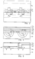
- the chip includes a semi-conductive substrate layer SC, a first dielectric layer DE 1 , a first conductive layer CN 1 , a second dielectric layer DE 2 , a second conductive layer CN 2 , an nth dilectric layer DE n and an nth conductive layer CN n .
- Diffusions S and D in the semiconductive substrate layer SC define sources and drains, which are combined with gate conductors G and interconnected by the first conductive layer CN 1 , to define complementary MOS field effect transistors that are arrayed to define the circuit elements of the chip 10.
- the first conductive layer CN 1 is coupled to a source S and a drain D by conductive contacts 30 through holes in the first dielectric layer DE 1 .
- the second conductive layer CN 2 is coupled to the first conductive layer CN 1 , by a contact 31 through a hole in the second dielectric layer DE 2 for conducting to the circuit elements a predetermined signal that is essential to an intended function of the shielded circuit elements.
- the second conductive layer CN 2 overlies the circuit elements to thereby define the secure area 11 in which the circuit elements are shielded from inspection.
- the chip includes a semiconductive substrate layer SC, a first dielectric layer DE 1 , a first conductive layer CN 1 , second dielectric layer CN 1 , an nth dielectric layer DE n , and an nth conductive layer CN n .
- Diffusions C, B and E in the semiconductive layer SC define collectors, bases and emitters which are interconnected by the first conductive layer CN 1 , to define bipolar transistors that are arrayed to define the circuit elements of the chip 10.
- the first conductive layer CN 1 is coupled to a collector C and a base B by conductive contacts 32 through holes in the first dieletric layer DE 1 for conducting to the circuit elements a predetermined signal that is essential to an intended function of the shielded circuit elements.
- the second conductive layer CN 2 is coupled to the first conductive layer CN 1 , by a contact 33 through a hole in the second dielectric layer DE 2 for conducting to the circuit elements a predetermined signal that is essential to an intended function of the shielded circuit elements.
- the second conductive layer CN 2 overlies the circuit elements to thereby define the secure area 11 in which the circuit elements are shielded from inspection.
- All circuit elements of the chip 10 that distribute, store, process or affect the processing of secure data utilise conductive layers, such as the interconnect layer CN 1 , that are fabricated before and lie under the conductive layer, such as layer CN 2 , which functions as a shield and thereby defines the boundaries of the secure area 11.
- conductive layers such as the interconnect layer CN 1
- layer CN 2 which functions as a shield and thereby defines the boundaries of the secure area 11.
- the second conductive layer CN 2 acts both as a shield to mechanical and SEM probing and as a predetermined essential signal carrying layer that cannot be removed without rendering the underlying circuit elements inoperable.
- the predetermined essential signal may be either a power signal or a control signal, such as an instruction.
- the predetermined essential signal is a power signal
- removal of the shield layer CN 2 by either mechanical, chemical or other means for inspection purposes will then remove power from the underlying circuit elements, rendering them inoperable and also possibly forcing the same circuit elements to lose any data or logic state stored therein.
- each of such memories M 1 , M 2 is covered by the second conductive layer CN 2 to shield the memories M 1 , M 2 from inspection; and a power signal is separately distributed to each of the memories M 1 , M 2 from the portion of the second conductive layer CN 2 that overlies the respective memory M 1 , M 2 .
- a power signal is separately distributed to each of the memories M 1 , M 2 from the portion of the second conductive layer CN 2 that overlies the respective memory M 1 , M 2 .
- Such distribution is shown in Figure 5, wherein the second conductive layer CN 2 is connected by a contact 34 to the source S of a transistor included in a volatile memory for providing power to the memory.
- Removal of the overlying portion of the second conductive layer CN 2 to enable inspection of the respective memory M 1 , M 2 results in power being removed from the respective memory M 1 , M 2 . Since the memory M 1 , M 2 is volatile, removal of power therefrom results in deletion of the secure data stored therein. Accordingly, an attempt to inspect the contents of either of the memories M 1 , M 2 by removing only the portion of the second conductive layer CN 2 that overlies such memory will be unavailing.
- power signals V CC are distributed from the second conductive layer CN 2 to a plurality of volatile memory elements M in a manner that takes up less space than in the embodiment described above, in which power is separately distributed to each of the memory elements M from only that portion of the second conductive layer as overlies such memory element M.
- each row of memory elements M receives power from the overlying second conductive layer CN 2 via a separate underlying first conductive layer CN 1 .
- the second conductive layer CN 2 is connected to the respective first conductive layer CN 1 by conductive contacts 35.
- any combination of conductive layers may be used in this arrangement.
- the use of the conductive layers most highly embedded within the vertical dimension of the chip as the shielding conductive layers results in the greatest security.
- the logic elements 26 and the memory 24 process and store nonsecure data and control signals.
- the non secure data and control signals are transferred from the nonsecure data bus 28 to the secure data bus 16 in the secure area 11 by the transfer logic circuit 18.
- the transfer logic circuit 18 transfers the nonsecure data and control signals to the secure data bus 16 within the secure area 11 for processing with the secure data by the microprocessor 14.
- the transfer logic circuit 18 enables the nonsecure data and the control signals to be transferred between the non secure data bus 28 and the secure data bus 16 in response to control signals generated by the microprocessor 14 that indicate when nonsecure data is present on the secure data bus 16.
- the microprocessor 14 monitors the status of the data signals on the secure data bus 16, and generates the control signals that enable the logic circuit 18 to transfer data signals and control signals between the nonsecure data bus 28 and the secure data bus 16 only during such times as nonsecure data is present on the secure data bus 16.
- the conductive layer CN 2 overlies the transfer logic circuit 18 in order to shield the transfer logic circuit from inspection.
- the conductive layer CN 2 also conducts a power signal to the transfer logic circuit 18, whereby removal of the conductive layer CN 2 for the purpose of inspecting the transfer logic circuit 18 results in power being removed from the transfer logic circuit 18 and prevents the logic circuit 18 from transferring any data or control signals between the secure data bus 16 and the nonsecure data bus 28.
- the microprocessor 14 provides memory access logic circuit, which enables data on the secure data bus 16 to be stored in the memories M 1 , M 2 , M n ; and the shielding conductive layer CN 2 conducts a power signal to the microprocessor 14.
- each of the shielding logic circuits 14, 18 in the secure area is separately coupled to only that portion of the shielding conductive layer CN 2 that overlies such logic circuit 14, 18 for receiving a power signal from only that overlying portion of the shielding conductive layer CN 2 .
- a secure signal is distributed in a conductive layer CN 1 , that underlies layers CN 2 and CN n , and shielding signals (such as essential control or power signals) are distributed in the overlying shield layers CN 2 and CN n , respectively.
- shielding signals such as essential control or power signals
- the boundaries of one shielding conductive layer CN n are shown in the drawing by solid lines, the boundaries of the other shielding conductive layer CN 2 are shown in the drawing by dashed lines, and the underlying conductive layer CN 1 is shown in the drawing by shading.
- the underlying conductive layer CN 1 is entirely shielded by either one or the other of the shielding conductive layers CN 2 and CN n and one portion of the underlying conductive layer CN 1 is shielded by both of the shielding conductive layers CN 2 and CN n .
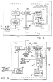
- the chip 10 includes a system for preventing the alteration of secure data stored in a predetermined memory location. Alternative embodiments of such a prevention system are shown in Figures 8 and 9.
- the system of Figure 8 includes a memory M, a memory control logic circuit 38, a decoder 40, a fuse element 42 and a fuse altering device 44.
- This system is applicable to and includes as the memory M, each of the memories M 1 , M 2 , M n in which secure data is stored.
- the memory M has a plurality of memory locations, with a predetermined location being for the storage of unalterable secure data from the data bus 16.
- the memory control logic circuit 38 is coupled to the memory M by an address bus 46 for causing data to be stored in locations of the memory M indicated by address signals provided on the address bus 46 when a "write" signal is provided on line 47 from the memory control logic circuit 38 to the secure memory M.
- the fuse element 42 has an initial state and an irreversibly altered state.
- fuse element refers to both fuses and antifuses.
- Fuse elements are formed in the chip 10 by the combination of a metallic conductive layer and a polysilicon conductive layer.
- Antifuse elements can be formed in the chip by metallic conductive layers, polysilicon conductive layers or a combination of both.
- Antifuse elements are formed by P + /N + semiconductor junction diodes and P - .N - semiconductor junction diodes formed in a semiconductive layer of the chip by conductor/oxide conductor structures or by conductor/amorphous silicon/conductor structures in the chip.
- the fuse altering device 44 is coupled to the fuse element 42 for irreversibly altering the state of the fuse element 42 in response to a predetermined control signal received on line 48 from a terminal 50 that is external to the secure area 11.
- the control signal on line 48 is received from a terminal (not shown) that is internal to the secure area 11.
- the decoder 40 is coupled to the fuse element 42, the memory control circuit 38 and the address bus 46 for monitoring the state of the fuse element 42 and the address signals on the address bus 46, and for preventing the memory control circuit 38 from causing data to be stored in the predetermined memory location of the memory M after the state of the fuse element 42 has been altered irreversibly whenever the predetermined memory location is indicated by an address signal on the address bus 46.
- the second conductive layer CN 2 shields the memory M, the memory control logic circuit 38, the decoder 40, and the fuse element 42 from direct external access.
- the memory M, the memory control logic circuit 38 and the decoder 40 are all coupled to the second conductive layer CN 2 so as to be powered by the power signal carried by the second conductive layer CN 2 .
- the system of Figure 8 is used to prevent the alteration of secure data initially stored in the predetermined locations of the memory M. Once the state of the fuse element 42 is irreversibly changed, the decoder 40 prevents the writing of any further data into the predetermined memory locations indicated by the address signals on the address bus 46.
- the fuse element 42 in the system of Figure 8 also may be connected to other shielded circuit elements (not shown) that perform or affect certain preliminary secure data processing functions that are applicable only prior to such time as the product that includes the chip is distributed to users of the product, such as preliminary processing of the secure data or the loading of instructions for processing the secure data.
- Means, such as the decoder 40, are coupled to the fuse element 42 and such other shielded circuit elements for monitoring the state of the fuse element and for preventing the intended function of such other shielded circuit element after the state of the fuse element has been altered irreversibly.
- fuse technologies allow fusing only at a foundry during the secure integrated circuit chip fabrication process. For example, certain foundries may require that an oxide be grown over a polysilicon (or other fuse material) after the fuse has been blown to afford better long term device reliability.
- the system of Figure 9 allows a separate manufacturer to load secure data into the secure memory M after foundry fusing, yet still prevents alteration of the contents of the memory M.
- the system of Figure 9 includes a memory M, an erasable memory 52, such as an EPROM or an EEROM (electrically erasable ROM), memory control logic circuit 54, an enabling circuit 55, a fuse element 56, an AND gate 57 and a fuse altering device 58.
- the memory control logic circuit 54 includes an AND gate 60, and N connections including wiring and inverters 62 that couple the AND gate 60 to the erasable memory 52.
- the inverters 62 are connected between selected inputs to the AND gate 60 and selected memory locations in the erasable memory 52 so as to define a predetermined data pattern in the erasable memory 52 that must be present to enable the AND gate 60.
- the memory M has a plurality of memory locations, with a predetermined location being for the storage of unalterable secure data.
- the enabling circuit 55 enables a data pattern to be stored in the erasable memory 52 when a write enable signal is applied on line 63 to the enabling circuit 55.
- the memory control logic circuit 54 couples the memory M to the erasable memory 52 in such a manner as to cause data to be stored in the predetermined location of the first memory M in response to a write signal on line 64 to the AND gate 60 whenever the erasable memory 52 contains a predetermined data pattern.
- the contents of the erasable memory 52 may be erased by providing an "erase" control signal at an erase terminal 66 located outside the secure area 11 of the chip 10.
- the fuse element 56 has an initial state and an irreversibly altered state.
- the fuse altering device 58 is coupled to the fuse element 56 for irreversibly altering the state of the fuse element 56 in response to a predetermined control signal received on line 67 from a terminal 68 that is external to the secure area 11.
- the control signal on line 67 is received from a terminal (not shown) that is internal to the secure area 11.
- a data pattern is provided at a data terminal 69 and fed into the erasable memory through the AND gate 57.
- the AND gate 57 has one input connected to the fuse element 56 so as to enable data to be written into the erasable memory 52 only while the fuse element 56 is in its initial state.
- the fuse element 56 also is coupled to the enabling circuit 55 so as to enable the predetermined data pattern to be stored in the erasable memory 52 only prior to the state of the fuse element 56 being irreversibly altered.
- N bits of erasable memory 52 are required.
- the predetermined pattern of ones and zeros corresponding to the pattern of inverters 62 coupling the erasable memory 52 to the AND gate 60 is loaded into the erasable memory 52 to enable the AND gate 60 to pass a "write" control signal on line 64 to the memory M.
- the state of the fuse element is irreversibly altered so that the predetermined pattern cannot be changed.
- processing and packaging of the integrated circuit chip 10 can continue, subject to the condition that the final processing and packaging steps do not disturb the stored predetermined pattern in the erasable memory 52.
- secure data can be stored in the secure memory M since the predetermined pattern stored in the erasable memory 52 matches the predetermined pattern hard-wired into the memory control logic circuit 54 by the inverters 62.
- an "erase” signal is applied to the erase terminal 66 to erase the contents of the erasable memory 52 and thereby prevent alteration of the secure data stored in the secure memory M.
- the second conductive layer CN 2 shields the memory M, the erasable memory 52, the memory control logic circuit 54, the enabling circuit 55 and the fuse element 56 from direct external access.
- This technique makes the system of Figure 9 secure from any attack short of an extremely precise X-ray beam or other complex means that may be used to remotely reprogram the erasable memory 52 through the covering layers of the chip 10.
- the security of this technique relies on the fact it is difficult to remotely reprogram the contents of an EEROM or EPROM, or to reconnect a blown fuse element. If a high power unfocused or diffuse X-ray or other means could essentially randomise the EEROM or EPROM contents, then an attacker could make repeated attempts to achieve the enabling pattern. Thus, security may also require that the EEROM or EPROM cells be designed to be biased in terms of their state, in other words, biased towards a preferred pattern of all ones or all zeros. Thus any unfocused beam would with high probability drive the contents to the preferred pattern rather than to the predetermined pattern that enables data to be stored in the memory M. Security can also be increased by using a longer predetermined pattern, with a larger number N of bits.
- the memory M, the erasable memory 52, the AND gate 60 and the enabling circuit 55 are all coupled to the second conductive layer CN 2 so as to be powered by the power signal carried by the second conductive layer CN2.
- the fuse element 56 in the system of Figure 9 also may be connected to other shielded circuit elements (not shown) that perform or affect certain preliminary secure data processing functions that are applicable only prior to such time as the product that includes the chip is distributed to users of the product, such as preliminary processing of the secure data or the loading of instructions for processing the secure data.
- the fuse element 56 is coupled to such other shielded circuit element so as to enable the intended function of such other shielded circuit element only prior to the state of the fuse element being irreversibly altered.
- Figure 10 shows a system for permanently disabling test signal paths after testing operations are completed, so that no further access to internal secure circuit elements from the external pins of the chip is possible.
- This system includes a fuse element 70, first and second inverters 72, 74, a resistance 75, first and second NAND gates 76, 78 and a fuse altering device 79.
- the fuse element 70 has a initial state and an irreversibly altered state.
- the fuse altering device 79 is coupled to the fuse element 70 for irreversibly altering the state of the fuse element 70 in response to a predetermined control signal received on line 80 from a terminal 81 that is external to the secure area 11.
- the control signal on line 80- is received from a terminal (not shown) that is internal to the secure area 11.
- the fuse element 70 is coupled to the first and second NAND gates 76, 78 so as to enable the secure areas of the chip 10 to be accessed for testing only prior to the state of the fuse element 70 being irreversibly altered.
- the fuse element 70 and the inverters 72, 74 are connected in series to one input to the first NAND gate 76.
- the output of the first NAND gate 76 is applied to an external test data output terminal 82.
- the fuse element 70 and the inverters 72, 74 are also connected in series to one input to the second NAND gate 78.
- the second NAND gate 78 passes a test command signal from an internal test command input terminal 84 to a test command input node 86 within the secure area 11 of the chip 10.
- Test data is provided at internal test data output node 88 within the secure area 11 of the chip 10 in response to a test command input signal being provided to the internal test command input node 86.
- the test data provided at the internal test data output terminal may be accessed from the secure circuit elements of the chip 10, such as the circuit elements 14, M 1, M 2 , M n , 16, 17, 18, 20 ( Figure 1).
- test data is provided from the internal test data output node 88 through the first NAND gate 76 to the external test data output terminal 82 only while the fuse element 70 is in its initial state.
- test command input signal is provided from the external test command input terminal 84 to the internal test command input node 86 only while the fuse is in its initial state.
- the second conductive layer CN 2 shields the fuse element 70, the inverters 72, 74, the resistor 75 and the NAND gates 76, 78 from direct external access.
- the inverters 72, 74, the resistor 75 and the NAND gates 76, 78 are all coupled to the second conductive layer CN 2 so as to be powered by the power signal carried by the second conductive layer CN 2 .
- the signal paths from the fuse element 70 to the first and second NAND gates 76, 78 are distributed primarily to an N+ or P+ diffusion.
- Polysilicon and other conductive layers may be used as well, with diminishing security. The use of the uppermost conductive layers CN n CN n-1 should be avoided.
Abstract
Description
- The present invention generally pertains to integrated circuit chips for electronic data processing systems and is particularly directed to preventing inspection and/or modification of secure data that is stored or processed within a secure area of an integrated circuit chip.
- Integrated circuit chips that process and store secure data include a secure area containing circuit elements for processing and storing the secure data, and a non secure area containing circuit elements for processing and storing non secure data and control signals. An integrated circuit chip contains a semi-conductive layer containing diffusions defining circuit element components; and a first conductive layer coupled to the semi-conductive layer to interconnect the components to thereby define the circuit elements. All modern integrated circuit chips include one or more conductive layers, typically for interconnecting circuit elements and components thereof. Generally these layers are used for both control signal and power signal distribution in a way that is intended to maximise signal interconnection density and reduce the area required for such interconnections.
- The secure area further contains circuit elements for transferring non secure data and control signals to a data bus within the secure area for processing with the secure data by data processing circuit elements within the secure area. Logic circuit elements within the secure area enable the nonsecure data and the control signals to be transferred between the non secure area and the data bus within the secure area in response to control signals generated by the data processing circuit elements within the secure area.
- Nevertheless, even though the secure data cannot be readily transferred in such an integrated circuit chip from the secure area to the non secure area, it is possible to gain access to secure data stored or being processed within the secure area by inspecting the secure area with such diagnostic tools as a scanning electron microscope (SEM) or a probe that couples an oscilloscope to a given node within the secure area from which the secure data can be accessed. Also, by delivering appropriate control signals to the logic circuit elements within the secure area by such means as a probe, it may be possible to cause the logic circuit to enable transfer of secure data to the nonsecure area from a data bus within the secure area that carries both nonsecure and secure data for processing by the data processing circuit elements within the secure area or to enable the secure data stored within the secure area to be replaced by clandestine data that would enable the intended security of the chip to be compromised.
- The present invention provides an integrated circuit chip containing a secure area in which secure data is processed and/or stored, comprising:
- a semiconductor layer containing diffusions defining circuit element components;
- a first conductive layer coupled to the semiconductor layer to interconnect the components to thereby define circuit elements for distributing, storing, processing and/or affecting the processing of secure data;
- a second conductive layer overlying the circuit elements to thereby define a secure
area in which the circuit elements are shielded from inspection, and coupled to the circuit
elements for conducting to the circuit elements a predetermined signal that is essential to
an intended function of the circuit elements, whereby removal of the second conductive
layer will prevent the predetermined essential signal from being provided to the circuit
elements and thereby prevent the intended function;
characterised in that the shielded circuit elements further comprise: - a fuse element having an initial state and an irreversibly altered state; and
- means coupled to the fuse element for irreversibly altering the state of the
fuse element in response to a predetermined control signal;
wherein the fuse element is coupled to another component of the chip such that irreversibly altering the state of the fuse element prevents some function of the chip. -
- The invention will now be described by way of example with reference to the drawings in which:-
- Figure 1 is a block diagram of an integrated circuit chip to which the present invention can be applied;
- Figure 2 is a cross-sectional view illustrating the shielding of MOS circuit element components in the Figure 1 integrated circuit chip;
- Figure 3 is a plan view illustrating the use of an overlying conductive layer to shield circuit element components and to conduct a predetermined signal to shielded MOS circuit elements;
- Figure 4 is a cross-sectional view illustrating the shielding of bipolar circuit element components in an integrated circuit chip;
- Figure 5 is a cross-sectional view illustrating the use of an overlying conductive layer to shield circuit elements and to conduct power to the shielded circuit elements;
- Figure 6 is a block diagram illustrating an alternative topology for shielding a plurality of volatile memories;
- Figure 7 is a plan view illustrating the use of an overlying conductive layer to carry a signal essential to the function of a circuit element;
- Figure 8 is a block diagram of a system in the secure area of the chip for preventing the alteration of secure data stored in a predetermined memory location in accordance with the present invention;
- Figure 9 is a block diagram of an alternative embodiment of a system in the secure area of the chip for preventing the alteration of secure data stored in a predetermined memory location; and
- Figure 10 is a block diagram of a system in the secure area of the chip for limiting when the secure area may be accessed for testing.
-
- Referring to Figure 1, a preferred
integrated circuit chip 10 with which the present invention may be used includes asecure area 11 and a nonsecure area 12. Thechip 10 is a VLSI (Very Large Scale Integrated) circuit chip. Within thesecure area 11, thechip 10 defines the following circuit elements: amicroprocessor 14 for processing secure data, a plurality of memories M1,M2,Mn for storing secure data, a secure data bus 16, a secure address bus 17,transfer logic circuits 18, and secure clock andpower control circuits 20. Thechip 10 need not be limited to such a specific mixture of circuit elements, but may contain any mixture of circuit elements wherein secure data is to be either protected against unauthorised attacks of reading out or modification of secure data and/or instructions. The memories M1, M2, Mn can be of any type, to wit: RAM (random-access memory), ROM (read-only memory), EPROM (electrically programmable ROM) EEPROM: (electrically erasable programmable ROM) and others, such as register files, FIFO (first-in/first-out) buffers, etc. - A conductive layer CN2 covers the
circuit elements 14, M1, M2, Mn, 16, 17, 18, 20 to shield such circuit elements from inspection, and thereby defines thesecure area 11. - Within the non
secure area 12, thechip 10 defines the following circuit elements. amemory 24, alogic circuit 26 and a nonsecure data bus 28. - In a
chip 10 including MOS circuit elements, as illustrated in Figures 2 and 3, the chip includes a semi-conductive substrate layer SC, a first dielectric layer DE1, a first conductive layer CN1, a second dielectric layer DE2, a second conductive layer CN2, an nth dilectric layer DEn and an nth conductive layer CNn. Diffusions S and D in the semiconductive substrate layer SC define sources and drains, which are combined with gate conductors G and interconnected by the first conductive layer CN1, to define complementary MOS field effect transistors that are arrayed to define the circuit elements of thechip 10. The first conductive layer CN1, is coupled to a source S and a drain D byconductive contacts 30 through holes in the first dielectric layer DE1. The second conductive layer CN2 is coupled to the first conductive layer CN1, by acontact 31 through a hole in the second dielectric layer DE2 for conducting to the circuit elements a predetermined signal that is essential to an intended function of the shielded circuit elements. - Removal of the second conductive layer CN2 will prevent the predetermined essential signal from being provided to the circuit elements and thereby prevent the intended function. The second conductive layer CN2 overlies the circuit elements to thereby define the
secure area 11 in which the circuit elements are shielded from inspection. - In a
chip 10 including bipolar elements, as illustrated in Figure 4, the chip includes a semiconductive substrate layer SC, a first dielectric layer DE1, a first conductive layer CN1, second dielectric layer CN1, an nth dielectric layer DEn, and an nth conductive layer CNn. Diffusions C, B and E in the semiconductive layer SC define collectors, bases and emitters which are interconnected by the first conductive layer CN1, to define bipolar transistors that are arrayed to define the circuit elements of thechip 10. The first conductive layer CN1, is coupled to a collector C and a base B byconductive contacts 32 through holes in the first dieletric layer DE1 for conducting to the circuit elements a predetermined signal that is essential to an intended function of the shielded circuit elements. The second conductive layer CN2 is coupled to the first conductive layer CN1, by acontact 33 through a hole in the second dielectric layer DE2 for conducting to the circuit elements a predetermined signal that is essential to an intended function of the shielded circuit elements. - Removal of the second conductive layer CN2 will prevent the predetermined essential signal from being provided to the circuit elements and thereby prevent the intended function. The second conductive layer CN2 overlies the circuit elements to thereby define the
secure area 11 in which the circuit elements are shielded from inspection. - All circuit elements of the
chip 10 that distribute, store, process or affect the processing of secure data utilise conductive layers, such as the interconnect layer CN1, that are fabricated before and lie under the conductive layer, such as layer CN2, which functions as a shield and thereby defines the boundaries of thesecure area 11. - The second conductive layer CN2 acts both as a shield to mechanical and SEM probing and as a predetermined essential signal carrying layer that cannot be removed without rendering the underlying circuit elements inoperable. The predetermined essential signal may be either a power signal or a control signal, such as an instruction. When the predetermined essential signal is a power signal, removal of the shield layer CN2 by either mechanical, chemical or other means for inspection purposes will then remove power from the underlying circuit elements, rendering them inoperable and also possibly forcing the same circuit elements to lose any data or logic state stored therein.
- The technique is particularly effective for protecting secure data stored in a volatile memory, such as a volatile RAM. In an embodiment of the
chip 10 in which the memories M1 and M2 are volatile memories, each of such memories M1, M2 is covered by the second conductive layer CN2 to shield the memories M1, M2 from inspection; and a power signal is separately distributed to each of the memories M1, M2 from the portion of the second conductive layer CN2 that overlies the respective memory M1, M2. Such distribution is shown in Figure 5, wherein the second conductive layer CN2 is connected by acontact 34 to the source S of a transistor included in a volatile memory for providing power to the memory. Removal of the overlying portion of the second conductive layer CN2 to enable inspection of the respective memory M1, M2 results in power being removed from the respective memory M1, M2. Since the memory M1, M2 is volatile, removal of power therefrom results in deletion of the secure data stored therein. Accordingly, an attempt to inspect the contents of either of the memories M1, M2 by removing only the portion of the second conductive layer CN2 that overlies such memory will be unavailing. - In an alternative arrangement shown in Figure 6, power signals VCC are distributed from the second conductive layer CN2 to a plurality of volatile memory elements M in a manner that takes up less space than in the embodiment described above, in which power is separately distributed to each of the memory elements M from only that portion of the second conductive layer as overlies such memory element M. In this arrangement each row of memory elements M receives power from the overlying second conductive layer CN2 via a separate underlying first conductive layer CN1. The second conductive layer CN2 is connected to the respective first conductive layer CN1 by
conductive contacts 35. Although this arrangement does trade off some security for area efficiency, an attempt to inspect these memory elements M without causing the data to be deleted by a power loss resulting from removal of the second conductive layer CN2 would require very high resolution removal of the second conductive layer CN2 while leaving intact all interlayerconductive contacts 35 and the portion of the second conductive layer CN2 that distributes power to thesecontacts 35. - Any combination of conductive layers may be used in this arrangement. The use of the conductive layers most highly embedded within the vertical dimension of the chip as the shielding conductive layers results in the greatest security.
- Referring again to Figure 1, within the non
secure area 12, thelogic elements 26 and thememory 24 process and store nonsecure data and control signals. The non secure data and control signals are transferred from the nonsecure data bus 28 to the secure data bus 16 in thesecure area 11 by thetransfer logic circuit 18. Thetransfer logic circuit 18 transfers the nonsecure data and control signals to the secure data bus 16 within thesecure area 11 for processing with the secure data by themicroprocessor 14. Thetransfer logic circuit 18 enables the nonsecure data and the control signals to be transferred between the non secure data bus 28 and the secure data bus 16 in response to control signals generated by themicroprocessor 14 that indicate when nonsecure data is present on the secure data bus 16. Themicroprocessor 14 monitors the status of the data signals on the secure data bus 16, and generates the control signals that enable thelogic circuit 18 to transfer data signals and control signals between the nonsecure data bus 28 and the secure data bus 16 only during such times as nonsecure data is present on the secure data bus 16. - As described above, the conductive layer CN2 overlies the
transfer logic circuit 18 in order to shield the transfer logic circuit from inspection. The conductive layer CN2 also conducts a power signal to thetransfer logic circuit 18, whereby removal of the conductive layer CN2 for the purpose of inspecting thetransfer logic circuit 18 results in power being removed from thetransfer logic circuit 18 and prevents thelogic circuit 18 from transferring any data or control signals between the secure data bus 16 and the nonsecure data bus 28. Likewise, removal of the conductive layer CN2 in order to allow control signals to be delivered to thetransfer logic circuit 18 by such means as a probe for enabling secure data to be transferred from thesecure area 11 to the nonsecure area 12 of thechip 10 will be unavailing since such removal of the shielding conductive layer CN2 also removes power from thetransfer logic circuit 18. - This technique may be extended in the reverse direction, so that clandestine data cannot be written into a secure memory M1, M2, Mn from the non
secure area 12. Themicroprocessor 14 provides memory access logic circuit, which enables data on the secure data bus 16 to be stored in the memories M1, M2, Mn; and the shielding conductive layer CN2 conducts a power signal to themicroprocessor 14. Thus removal of the shielding conductive layer CN2 in order to deliver control signals to the memory access logic circuit of themicroprocessor 14 that would enable clandestine data to be substituted in the memories of M1, M2, Mn for the secure data to thereby compromise the intended security of the chip would be unavailing since removal of the shielding conductive layer CN2 removes power from themicroprocessor 14 and thereby prevents the memory access logic circuit therein from enabling data to be stored in the memories M1, M2, Mn. - In one example each of the shielding
logic circuits such logic circuit - In an example shown in Figure 7, a secure signal is distributed in a conductive layer CN1, that underlies layers CN2 and CNn, and shielding signals (such as essential control or power signals) are distributed in the overlying shield layers CN2 and CNn, respectively. The boundaries of one shielding conductive layer CNn, are shown in the drawing by solid lines, the boundaries of the other shielding conductive layer CN2 are shown in the drawing by dashed lines, and the underlying conductive layer CN1 is shown in the drawing by shading. The underlying conductive layer CN1 is entirely shielded by either one or the other of the shielding conductive layers CN2 and CNn and one portion of the underlying conductive layer CN1 is shielded by both of the shielding conductive layers CN2 and CNn.
- An attempt at cutting through the shield layers CN2 and Cnn with chemicals or conventional lasers or microprobes to gain access to the secure signal in the conductive layer CN1 results either in the conductive layer CN1 becoming connected (shorted) to the shield layers CN2 and CNn or in an open circuit being created in the circuit paths defined by the conductive layers CN1, CN2, CNn, which thereby disrupts distribution of the secure signal and the essential signals and alters the intended functions of the circuit elements connected to the conductive layers CN1, CN2 and CNn so as to impair the intended function of the
chip 10. - It is critically important that certain secure data stored in the
chip 10 during formation of a product that includes the chip not be modified after the storage of such secure data. To accomplish this purpose thechip 10 includes a system for preventing the alteration of secure data stored in a predetermined memory location. Alternative embodiments of such a prevention system are shown in Figures 8 and 9. - The system of Figure 8 includes a memory M, a memory
control logic circuit 38, adecoder 40, afuse element 42 and afuse altering device 44. This system is applicable to and includes as the memory M, each of the memories M1, M2, Mn in which secure data is stored. - The memory M has a plurality of memory locations, with a predetermined location being for the storage of unalterable secure data from the data bus 16.
- The memory
control logic circuit 38 is coupled to the memory M by anaddress bus 46 for causing data to be stored in locations of the memory M indicated by address signals provided on theaddress bus 46 when a "write" signal is provided online 47 from the memorycontrol logic circuit 38 to the secure memory M. - The
fuse element 42 has an initial state and an irreversibly altered state. The term "fuse element" refers to both fuses and antifuses. Fuse elements are formed in thechip 10 by the combination of a metallic conductive layer and a polysilicon conductive layer. Antifuse elements can be formed in the chip by metallic conductive layers, polysilicon conductive layers or a combination of both. Antifuse elements are formed by P+/N+ semiconductor junction diodes and P-.N- semiconductor junction diodes formed in a semiconductive layer of the chip by conductor/oxide conductor structures or by conductor/amorphous silicon/conductor structures in the chip. - The
fuse altering device 44 is coupled to thefuse element 42 for irreversibly altering the state of thefuse element 42 in response to a predetermined control signal received online 48 from a terminal 50 that is external to thesecure area 11. Alternatively, the control signal online 48 is received from a terminal (not shown) that is internal to thesecure area 11. - The
decoder 40 is coupled to thefuse element 42, thememory control circuit 38 and theaddress bus 46 for monitoring the state of thefuse element 42 and the address signals on theaddress bus 46, and for preventing thememory control circuit 38 from causing data to be stored in the predetermined memory location of the memory M after the state of thefuse element 42 has been altered irreversibly whenever the predetermined memory location is indicated by an address signal on theaddress bus 46. - The second conductive layer CN2 shields the memory M, the memory
control logic circuit 38, thedecoder 40, and thefuse element 42 from direct external access. - The memory M, the memory
control logic circuit 38 and thedecoder 40 are all coupled to the second conductive layer CN2 so as to be powered by the power signal carried by the second conductive layer CN2. - The system of Figure 8 is used to prevent the alteration of secure data initially stored in the predetermined locations of the memory M. Once the state of the
fuse element 42 is irreversibly changed, thedecoder 40 prevents the writing of any further data into the predetermined memory locations indicated by the address signals on theaddress bus 46. - The
fuse element 42 in the system of Figure 8 also may be connected to other shielded circuit elements (not shown) that perform or affect certain preliminary secure data processing functions that are applicable only prior to such time as the product that includes the chip is distributed to users of the product, such as preliminary processing of the secure data or the loading of instructions for processing the secure data. Means, such as thedecoder 40, are coupled to thefuse element 42 and such other shielded circuit elements for monitoring the state of the fuse element and for preventing the intended function of such other shielded circuit element after the state of the fuse element has been altered irreversibly. - Many fuse technologies allow fusing only at a foundry during the secure integrated circuit chip fabrication process. For example, certain foundries may require that an oxide be grown over a polysilicon (or other fuse material) after the fuse has been blown to afford better long term device reliability. The system of Figure 9 allows a separate manufacturer to load secure data into the secure memory M after foundry fusing, yet still prevents alteration of the contents of the memory M.
- The system of Figure 9 includes a memory M, an
erasable memory 52, such as an EPROM or an EEROM (electrically erasable ROM), memorycontrol logic circuit 54, an enablingcircuit 55, afuse element 56, an ANDgate 57 and afuse altering device 58. The memorycontrol logic circuit 54 includes an ANDgate 60, and N connections including wiring andinverters 62 that couple the ANDgate 60 to theerasable memory 52. Theinverters 62 are connected between selected inputs to the ANDgate 60 and selected memory locations in theerasable memory 52 so as to define a predetermined data pattern in theerasable memory 52 that must be present to enable the ANDgate 60. - The memory M has a plurality of memory locations, with a predetermined location being for the storage of unalterable secure data.
- The enabling
circuit 55 enables a data pattern to be stored in theerasable memory 52 when a write enable signal is applied online 63 to the enablingcircuit 55. - The memory
control logic circuit 54 couples the memory M to theerasable memory 52 in such a manner as to cause data to be stored in the predetermined location of the first memory M in response to a write signal online 64 to the ANDgate 60 whenever theerasable memory 52 contains a predetermined data pattern. - The contents of the
erasable memory 52 may be erased by providing an "erase" control signal at an erase terminal 66 located outside thesecure area 11 of thechip 10. - The
fuse element 56 has an initial state and an irreversibly altered state. Thefuse altering device 58 is coupled to thefuse element 56 for irreversibly altering the state of thefuse element 56 in response to a predetermined control signal received on line 67 from a terminal 68 that is external to thesecure area 11. Alternatively, the control signal on line 67 is received from a terminal (not shown) that is internal to thesecure area 11. - A data pattern is provided at a
data terminal 69 and fed into the erasable memory through the ANDgate 57. The ANDgate 57 has one input connected to thefuse element 56 so as to enable data to be written into theerasable memory 52 only while thefuse element 56 is in its initial state. - The
fuse element 56 also is coupled to the enablingcircuit 55 so as to enable the predetermined data pattern to be stored in theerasable memory 52 only prior to the state of thefuse element 56 being irreversibly altered. - N bits of
erasable memory 52 are required. At the foundry, the predetermined pattern of ones and zeros corresponding to the pattern ofinverters 62 coupling theerasable memory 52 to the ANDgate 60 is loaded into theerasable memory 52 to enable the ANDgate 60 to pass a "write" control signal online 64 to the memory M. After the predetermined pattern of ones and zeros is loaded into theerasable memory 52, the state of the fuse element is irreversibly altered so that the predetermined pattern cannot be changed. At this point, processing and packaging of theintegrated circuit chip 10 can continue, subject to the condition that the final processing and packaging steps do not disturb the stored predetermined pattern in theerasable memory 52. - After the
chip 10 is shipped to a separate manufacturer, secure data can be stored in the secure memory M since the predetermined pattern stored in theerasable memory 52 matches the predetermined pattern hard-wired into the memorycontrol logic circuit 54 by theinverters 62. - Once the secure data is stored in the secure memory M, an "erase" signal is applied to the erase terminal 66 to erase the contents of the
erasable memory 52 and thereby prevent alteration of the secure data stored in the secure memory M. - The second conductive layer CN2 shields the memory M, the
erasable memory 52, the memorycontrol logic circuit 54, the enablingcircuit 55 and thefuse element 56 from direct external access. - This technique makes the system of Figure 9 secure from any attack short of an extremely precise X-ray beam or other complex means that may be used to remotely reprogram the
erasable memory 52 through the covering layers of thechip 10. The security of this technique relies on the fact it is difficult to remotely reprogram the contents of an EEROM or EPROM, or to reconnect a blown fuse element. If a high power unfocused or diffuse X-ray or other means could essentially randomise the EEROM or EPROM contents, then an attacker could make repeated attempts to achieve the enabling pattern. Thus, security may also require that the EEROM or EPROM cells be designed to be biased in terms of their state, in other words, biased towards a preferred pattern of all ones or all zeros. Thus any unfocused beam would with high probability drive the contents to the preferred pattern rather than to the predetermined pattern that enables data to be stored in the memory M. Security can also be increased by using a longer predetermined pattern, with a larger number N of bits. - The memory M, the
erasable memory 52, the ANDgate 60 and the enablingcircuit 55 are all coupled to the second conductive layer CN2 so as to be powered by the power signal carried by the second conductive layer CN2. - The
fuse element 56 in the system of Figure 9 also may be connected to other shielded circuit elements (not shown) that perform or affect certain preliminary secure data processing functions that are applicable only prior to such time as the product that includes the chip is distributed to users of the product, such as preliminary processing of the secure data or the loading of instructions for processing the secure data. Thefuse element 56 is coupled to such other shielded circuit element so as to enable the intended function of such other shielded circuit element only prior to the state of the fuse element being irreversibly altered. - The secure data alteration prevention systems of Figures 8 and 9 are the subject of a commonly assigned patent EP-A-0378307 filed 4 January 1990, entitled "Prevention of Alteration of Data Stored in Secure Integrated Circuit Chip Memory".
- Manufacturing of complex integrated circuit chips requires complete access to the internal circuit elements during testing operations to insure that all included circuit elements work correctly. However, high accessibility for testing purposes generally is a security weakness for chips containing secure data or data which should not be modified.
- Figure 10 shows a system for permanently disabling test signal paths after testing operations are completed, so that no further access to internal secure circuit elements from the external pins of the chip is possible. This system includes a
fuse element 70, first andsecond inverters resistance 75, first andsecond NAND gates fuse altering device 79. - The
fuse element 70 has a initial state and an irreversibly altered state. Thefuse altering device 79 is coupled to thefuse element 70 for irreversibly altering the state of thefuse element 70 in response to a predetermined control signal received online 80 from a terminal 81 that is external to thesecure area 11. Alternatively, the control signal on line 80- is received from a terminal (not shown) that is internal to thesecure area 11. - The
fuse element 70 is coupled to the first andsecond NAND gates chip 10 to be accessed for testing only prior to the state of thefuse element 70 being irreversibly altered. - The
fuse element 70 and theinverters first NAND gate 76. The output of thefirst NAND gate 76 is applied to an external testdata output terminal 82. - The
fuse element 70 and theinverters second NAND gate 78. - The
second NAND gate 78 passes a test command signal from an internal testcommand input terminal 84 to a testcommand input node 86 within thesecure area 11 of thechip 10. Test data is provided at internal testdata output node 88 within thesecure area 11 of thechip 10 in response to a test command input signal being provided to the internal testcommand input node 86. The test data provided at the internal test data output terminal may be accessed from the secure circuit elements of thechip 10, such as thecircuit elements 14, M1, M2, Mn, 16, 17, 18, 20 (Figure 1). - The test data is provided from the internal test
data output node 88 through thefirst NAND gate 76 to the external testdata output terminal 82 only while thefuse element 70 is in its initial state. - Also, the test command input signal is provided from the external test
command input terminal 84 to the internal testcommand input node 86 only while the fuse is in its initial state. - The second conductive layer CN2 shields the
fuse element 70, theinverters resistor 75 and theNAND gates - The
inverters resistor 75 and theNAND gates - Additional protection is afforded by burying the signal paths from the
fuse element 70 to the first andsecond NAND gates chip 10 as possible to further preclude probe attacks. Therefore, the signal paths from thefuse element 70 to the first andsecond NAND gates
Claims (4)
- An integrated circuit chip (10) containing a secure area (11) in which secure data is processed and/or stored, comprisinga semiconductor layer (SC) containing diffusions (S,D) defining circuit element components;a first conductive layer (CN1) coupled to the semiconductor layer to interconnect the components to thereby define circuit elements (14, 16, 17, 18, 20, M1, M2, Mn) for distributing, storing, processing and/or affecting the procesing of secure data;a second conductive layer (CN2) overlying the circuit elements to thereby define a secure area (11) in which the circuit elements are shielded from inspection, and coupled to the circuit elements for conducting to the circuit elements a predetermined signal that is essential to an intended function of the circuit elements, whereby removal of the second conductive layer will prevent the predetermined essential signal from being provided to the circuit elements and thereby prevent the intended function;
characterised in that the shielded circuit elements further comprise:a fuse element (42, 57, 70) having an initial state and an irreversibly altered state; andmeans (44, 58, 79) coupled to the fuse element for irreversibly altering the state of the fuse element in response to a predetermined control signal;
wherein the fuse element is coupled to another component of the chip such that irreversibly altering the state of the fuse element prevents some function of the chip. - An integrated circuit chip according to Claim 1, characterised in that the shielded circuit elements comprise means (60) for enabling said storage of secure data; and that the fuse element (56) is coupled to the enabling means so as to enable said secure data storage only prior to the state of the fuse element being irreversibly altered.
- An integrated circuit chip according to Claim 1, further comprising:means (78) for accessing said circuit elements for testing said circuit elements;
characterised by the fuse element (70) being coupled to the accessing means so as to enable said access for testing only prior to the state of the fuse element being irreversibly altered. - An integrated circuit chip according to Claim 1, characterised in that the shielded circuit elements comprise:a given circuit element (M) that stores, processes or affects the processing of secure data; andmeans coupled to the fuse element (42) and the given circuit element (M) for monitoring the state of the fuse element and for preventing the intended function of the given circuit element after the state of the fuse element has been irreversibly altered.
Applications Claiming Priority (3)
| Application Number | Priority Date | Filing Date | Title |
|---|---|---|---|
| US07/297,472 US4933898A (en) | 1989-01-12 | 1989-01-12 | Secure integrated circuit chip with conductive shield |
| EP90300090A EP0378306B1 (en) | 1989-01-12 | 1990-01-04 | Secure integrated circuit chip with conductive shield |
| US297472 | 1994-08-29 |
Related Parent Applications (1)
| Application Number | Title | Priority Date | Filing Date |
|---|---|---|---|
| EP90300090A Division EP0378306B1 (en) | 1989-01-12 | 1990-01-04 | Secure integrated circuit chip with conductive shield |
Publications (3)
| Publication Number | Publication Date |
|---|---|
| EP0920057A2 true EP0920057A2 (en) | 1999-06-02 |
| EP0920057A3 EP0920057A3 (en) | 2000-01-12 |
| EP0920057B1 EP0920057B1 (en) | 2004-01-02 |
Family
ID=23146461
Family Applications (2)
| Application Number | Title | Priority Date | Filing Date |
|---|---|---|---|
| EP90300090A Expired - Lifetime EP0378306B1 (en) | 1989-01-12 | 1990-01-04 | Secure integrated circuit chip with conductive shield |
| EP99102130A Expired - Lifetime EP0920057B1 (en) | 1989-01-12 | 1990-01-04 | Secure integrated chip with conductive shield |
Family Applications Before (1)
| Application Number | Title | Priority Date | Filing Date |
|---|---|---|---|
| EP90300090A Expired - Lifetime EP0378306B1 (en) | 1989-01-12 | 1990-01-04 | Secure integrated circuit chip with conductive shield |
Country Status (11)
| Country | Link |
|---|---|
| US (1) | US4933898A (en) |
| EP (2) | EP0378306B1 (en) |
| JP (1) | JPH0787237B2 (en) |
| KR (1) | KR0180521B1 (en) |
| AU (1) | AU617026B2 (en) |
| CA (1) | CA2007469C (en) |
| DE (2) | DE69034125T2 (en) |
| DK (2) | DK0378306T3 (en) |
| ES (2) | ES2214760T3 (en) |
| IE (1) | IE62793B1 (en) |
| NO (2) | NO303808B1 (en) |
Cited By (12)
| Publication number | Priority date | Publication date | Assignee | Title |
|---|---|---|---|---|
| DE19681689C2 (en) * | 1995-12-20 | 2001-05-10 | Intel Corp | Method for producing a secured semiconductor component with analysis protection |
| WO2002059968A2 (en) * | 2001-01-24 | 2002-08-01 | Hrl Laboratories, Llc | Integrated circuits protected against reverse engineering using an apparent metal contact line terminating on field oxide and method |
| EP1229551A2 (en) * | 2000-11-09 | 2002-08-07 | Texas Instruments Incorporated | Method and apparatus for storing data in an integrated circuit |
| US6740942B2 (en) | 2001-06-15 | 2004-05-25 | Hrl Laboratories, Llc. | Permanently on transistor implemented using a double polysilicon layer CMOS process with buried contact |
| US6774413B2 (en) | 2001-06-15 | 2004-08-10 | Hrl Laboratories, Llc | Integrated circuit structure with programmable connector/isolator |
| US6815816B1 (en) | 2000-10-25 | 2004-11-09 | Hrl Laboratories, Llc | Implanted hidden interconnections in a semiconductor device for preventing reverse engineering |
| US6937512B2 (en) | 2000-09-28 | 2005-08-30 | Kabushiki Kaisha Toshiba | Nonvolatile semiconductor memory device with a ROM block settable in the write or erase inhibit mode |
| EP1674875A1 (en) * | 2004-12-14 | 2006-06-28 | St Microelectronics S.A. | Invalidation of an integrated circuit |
| US7935603B1 (en) | 2004-06-29 | 2011-05-03 | Hrl Laboratories, Llc | Symmetric non-intrusive and covert technique to render a transistor permanently non-operable |
| US8258583B1 (en) | 2002-09-27 | 2012-09-04 | Hrl Laboratories, Llc | Conductive channel pseudo block process and circuit to inhibit reverse engineering |
| US8679908B1 (en) | 2002-11-22 | 2014-03-25 | Hrl Laboratories, Llc | Use of silicide block process to camouflage a false transistor |
| DE102020202721A1 (en) | 2020-03-03 | 2021-09-09 | Infineon Technologies Ag | DATA STORAGE AND PROCEDURE FOR PROVIDING ITSELF |
Families Citing this family (94)
| Publication number | Priority date | Publication date | Assignee | Title |
|---|---|---|---|---|
| US5185717A (en) * | 1988-08-05 | 1993-02-09 | Ryoichi Mori | Tamper resistant module having logical elements arranged in multiple layers on the outer surface of a substrate to protect stored information |
| US5502315A (en) * | 1989-09-07 | 1996-03-26 | Quicklogic Corporation | Electrically programmable interconnect structure having a PECVD amorphous silicon element |
| US5989943A (en) * | 1989-09-07 | 1999-11-23 | Quicklogic Corporation | Method for fabrication of programmable interconnect structure |
| US5027397A (en) * | 1989-09-12 | 1991-06-25 | International Business Machines Corporation | Data protection by detection of intrusion into electronic assemblies |
| US5237610A (en) * | 1990-02-01 | 1993-08-17 | Scientific-Atlanta, Inc. | Independent external security module for a digitally upgradeable television signal decoder |
| US5029207A (en) * | 1990-02-01 | 1991-07-02 | Scientific-Atlanta, Inc. | External security module for a television signal decoder |
| US5199008A (en) * | 1990-03-14 | 1993-03-30 | Southwest Research Institute | Device for digitally measuring intervals of time |
| US5614756A (en) * | 1990-04-12 | 1997-03-25 | Actel Corporation | Metal-to-metal antifuse with conductive |
| US5381035A (en) * | 1992-09-23 | 1995-01-10 | Chen; Wenn-Jei | Metal-to-metal antifuse including etch stop layer |
| US5780323A (en) * | 1990-04-12 | 1998-07-14 | Actel Corporation | Fabrication method for metal-to-metal antifuses incorporating a tungsten via plug |
| US5181096A (en) * | 1990-04-12 | 1993-01-19 | Actel Corporation | Electrically programmable antifuse incorporating dielectric and amorphous silicon interlayer |
| US5270983A (en) * | 1990-09-13 | 1993-12-14 | Ncr Corporation | Single element security fusible link |
| US5086410A (en) * | 1990-09-14 | 1992-02-04 | National Semiconductor Corporation | Non-erasable eprom cell for redundancy circuit |
| US5053992A (en) * | 1990-10-04 | 1991-10-01 | General Instrument Corporation | Prevention of inspection of secret data stored in encapsulated integrated circuit chip |
| JP2960560B2 (en) | 1991-02-28 | 1999-10-06 | 株式会社日立製作所 | Microelectronic equipment |
| FR2674060B1 (en) * | 1991-03-14 | 1993-05-28 | Gemplus Card Int | PROGRAMMING METHOD FOR INTEGRATED MEMORY, PARTICULARLY FOR MEMORY CARD. |
| US5701027A (en) * | 1991-04-26 | 1997-12-23 | Quicklogic Corporation | Programmable interconnect structures and programmable integrated circuits |
| US5557136A (en) * | 1991-04-26 | 1996-09-17 | Quicklogic Corporation | Programmable interconnect structures and programmable integrated circuits |
| US5072331A (en) * | 1991-04-26 | 1991-12-10 | Hughes Aircraft Company | Secure circuit structure |
| US5196724A (en) * | 1991-04-26 | 1993-03-23 | Quicklogic Corporation | Programmable interconnect structures and programmable integrated circuits |
| AU1904992A (en) * | 1991-05-10 | 1992-12-30 | Quicklogic Corporation | Amorphous silicon antifuses and methods for fabrication thereof |
| US5302546A (en) * | 1991-07-31 | 1994-04-12 | Quicklogic Corporation | Programming of antifuses |
| US5327024A (en) * | 1992-07-02 | 1994-07-05 | Quicklogic Corporation | Field programmable antifuse device and programming method therefor |
| US5243226A (en) * | 1991-07-31 | 1993-09-07 | Quicklogic Corporation | Programming of antifuses |
| US5544070A (en) * | 1991-07-31 | 1996-08-06 | Quicklogic Corporation | Programmed programmable device and method for programming antifuses of a programmable device |
| KR940005696B1 (en) * | 1991-11-25 | 1994-06-22 | 현대전자산업 주식회사 | Rom device with security |
| US5233563A (en) * | 1992-01-13 | 1993-08-03 | Ncr Corporation | Memory security device |
| US5327497A (en) * | 1992-06-04 | 1994-07-05 | Integrated Technologies Of America, Inc. | Preboot protection of unauthorized use of programs and data with a card reader interface |
| US5610981A (en) * | 1992-06-04 | 1997-03-11 | Integrated Technologies Of America, Inc. | Preboot protection for a data security system with anti-intrusion capability |
| US5293133A (en) * | 1992-08-27 | 1994-03-08 | Quicklogic Corporation | Method of determining an electrical characteristic of an antifuse and apparatus therefor |
| KR100310220B1 (en) * | 1992-09-14 | 2001-12-17 | 엘란 티본 | Apparatus for manufacturing integrated circuit device and its manufacturing method |
| US5465341A (en) * | 1992-10-23 | 1995-11-07 | Vlsi Technology, Inc. | Verifiable security circuitry for preventing unauthorized access to programmed read only memory |
| US5444780A (en) * | 1993-07-22 | 1995-08-22 | International Business Machines Corporation | Client/server based secure timekeeping system |
| US5394106A (en) * | 1993-08-31 | 1995-02-28 | Gadzoox Microsystems | Apparatus and method for synthesis of signals with programmable periods |
| IL106892A0 (en) * | 1993-09-02 | 1993-12-28 | Pierre Badehi | Methods and apparatus for producing integrated circuit devices |
| US5533123A (en) * | 1994-06-28 | 1996-07-02 | National Semiconductor Corporation | Programmable distributed personal security |
| US6117707A (en) * | 1994-07-13 | 2000-09-12 | Shellcase Ltd. | Methods of producing integrated circuit devices |
| US5552720A (en) * | 1994-12-01 | 1996-09-03 | Quicklogic Corporation | Method for simultaneous programming of multiple antifuses |
| US5535168A (en) * | 1994-12-01 | 1996-07-09 | Motorola, Inc. | Method and apparatus for selectively erasing memory to extend battery life |
| US5495181A (en) * | 1994-12-01 | 1996-02-27 | Quicklogic Corporation | Integrated circuit facilitating simultaneous programming of multiple antifuses |
| AU6762296A (en) * | 1995-07-20 | 1997-02-18 | Dallas Semiconductor Corporation | Microcircuit with memory that is protected by both hardware and software |
| US5861652A (en) * | 1996-03-28 | 1999-01-19 | Symbios, Inc. | Method and apparatus for protecting functions imbedded within an integrated circuit from reverse engineering |
| US5602053A (en) * | 1996-04-08 | 1997-02-11 | Chartered Semidconductor Manufacturing Pte, Ltd. | Method of making a dual damascene antifuse structure |
| DE19634135C2 (en) * | 1996-08-23 | 1998-07-02 | Siemens Ag | Semiconductor circuit, in particular for use in an integrated module |
| DE19639033C1 (en) | 1996-09-23 | 1997-08-07 | Siemens Ag | Copy prevention arrangement for semiconductor chip |
| US5898776A (en) * | 1996-11-21 | 1999-04-27 | Quicklogic Corporation | Security antifuse that prevents readout of some but not other information from a programmed field programmable gate array |
| US5959466A (en) * | 1997-01-31 | 1999-09-28 | Actel Corporation | Field programmable gate array with mask programmed input and output buffers |
| US5861662A (en) * | 1997-02-24 | 1999-01-19 | General Instrument Corporation | Anti-tamper bond wire shield for an integrated circuit |
| US6150837A (en) * | 1997-02-28 | 2000-11-21 | Actel Corporation | Enhanced field programmable gate array |
| JPH1116365A (en) * | 1997-06-20 | 1999-01-22 | Oki Micro Design Miyazaki:Kk | Address decoder, semiconductor memory device and semiconductor device |
| US7743262B2 (en) * | 1997-07-15 | 2010-06-22 | Silverbrook Research Pty Ltd | Integrated circuit incorporating protection from power supply attacks |
| US7249109B1 (en) * | 1997-07-15 | 2007-07-24 | Silverbrook Research Pty Ltd | Shielding manipulations of secret data |
| US7249108B1 (en) * | 1997-07-15 | 2007-07-24 | Silverbrook Research Pty Ltd | Validation protocol and system |
| US7246098B1 (en) * | 1997-07-15 | 2007-07-17 | Silverbrook Research Pty Ltd | Consumable authentication protocol and system |
| US6137318A (en) * | 1997-12-09 | 2000-10-24 | Oki Electric Industry Co., Ltd. | Logic circuit having dummy MOS transistor |
| DE19810730A1 (en) * | 1998-03-12 | 1999-09-16 | Philips Patentverwaltung | Microcontroller circuit, esp. for identification systems such as cash cards, locking systems etc. |
| US6140212A (en) * | 1998-06-01 | 2000-10-31 | Motorola, Inc. | Semiconductor device and method therefor |
| US6816968B1 (en) * | 1998-07-10 | 2004-11-09 | Silverbrook Research Pty Ltd | Consumable authentication protocol and system |
| KR100396064B1 (en) * | 1998-08-18 | 2003-08-27 | 인피니언 테크놀로지스 아게 | Semiconductor chip with surface coating |
| EP0981162B1 (en) * | 1998-08-19 | 2007-03-07 | Infineon Technologies AG | Semiconductor chip with surface cover against optical inspection of the circuit structure |
| JP2000311943A (en) | 1999-04-27 | 2000-11-07 | Mitsubishi Electric Corp | Semiconductor device |
| DE59914555D1 (en) * | 1999-06-01 | 2007-12-27 | Infineon Technologies Ag | protection circuit |
| EP1063589A1 (en) * | 1999-06-25 | 2000-12-27 | TELEFONAKTIEBOLAGET L M ERICSSON (publ) | Device for processing data and corresponding method |
| JP3454471B2 (en) * | 1999-07-09 | 2003-10-06 | 沖電気工業株式会社 | Semiconductor device |
| US6225652B1 (en) * | 1999-08-02 | 2001-05-01 | Clear Logic, Inc. | Vertical laser fuse structure allowing increased packing density |
| US6518823B1 (en) * | 1999-08-31 | 2003-02-11 | Sony Computer Entertainment Inc. | One-time programmable logic device |
| EP1102320B1 (en) * | 1999-11-16 | 2008-08-20 | Infineon Technologies AG | Security ROM memory cell and manufacturing method therefor |
| US7005733B2 (en) * | 1999-12-30 | 2006-02-28 | Koemmerling Oliver | Anti tamper encapsulation for an integrated circuit |
| US6515304B1 (en) | 2000-06-23 | 2003-02-04 | International Business Machines Corporation | Device for defeating reverse engineering of integrated circuits by optical means |
| DE10044837C1 (en) * | 2000-09-11 | 2001-09-13 | Infineon Technologies Ag | Tampering detection circuit for IC has detection circuit coupled to signal line and at least one line pair extending between separate circuit blocks of IC |
| DE10058078C1 (en) * | 2000-11-23 | 2002-04-11 | Infineon Technologies Ag | Integrated circuit with analyzer protection has gaps left by first group of conducting tracks in wiring plane and filled by second group of conducting tracks provided for protection of IC |
| DE10065339B4 (en) * | 2000-12-27 | 2004-04-15 | Infineon Technologies Ag | Capacitive sensor as a protective device against attacks on a security chip |
| AU2003293540A1 (en) | 2002-12-13 | 2004-07-09 | Raytheon Company | Integrated circuit modification using well implants |
| EP1514166B1 (en) * | 2003-04-15 | 2012-01-11 | NDS Limited | Secure clock |
| JP4758621B2 (en) * | 2003-08-28 | 2011-08-31 | パナソニック株式会社 | Basic cell, end cell, wiring shape, wiring method, shield wire wiring structure |
| FR2864667B1 (en) * | 2003-12-29 | 2006-02-24 | Commissariat Energie Atomique | PROTECTING AN INTEGRATED CIRCUIT CHIP CONTAINING CONFIDENTIAL DATA |
| FR2868577A1 (en) | 2004-03-31 | 2005-10-07 | St Microelectronics Sa | DEVICE FOR DETECTING THE ATTACK OF AN INTEGRATED CIRCUIT CHIP |
| US7015823B1 (en) * | 2004-10-15 | 2006-03-21 | Systran Federal Corporation | Tamper resistant circuit boards |
| DE102005005622B4 (en) * | 2005-02-08 | 2008-08-21 | Infineon Technologies Ag | Security chip stack and a method for producing a security chip stack |
| US7281667B2 (en) * | 2005-04-14 | 2007-10-16 | International Business Machines Corporation | Method and structure for implementing secure multichip modules for encryption applications |
| FR2888975B1 (en) * | 2005-07-21 | 2007-09-07 | Atmel Corp | SECURITY METHOD FOR DATA PROTECTION |
| FR2893436B1 (en) * | 2005-11-15 | 2008-02-15 | Oberthur Card Syst Sa | SECURING BETWEEN ELECTRONIC COMPONENTS OF A PORTABLE SECURE ELECTRONIC ENTITY |
| US20070150754A1 (en) * | 2005-12-22 | 2007-06-28 | Pauly Steven J | Secure software system and method for a printer |
| US7623378B1 (en) * | 2006-05-02 | 2009-11-24 | Lattice Semiconductor Corporation | Selective programming of non-volatile memory facilitated by security fuses |
| US8168487B2 (en) | 2006-09-28 | 2012-05-01 | Hrl Laboratories, Llc | Programmable connection and isolation of active regions in an integrated circuit using ambiguous features to confuse a reverse engineer |
| US8255702B1 (en) * | 2009-12-03 | 2012-08-28 | Altera Corporation | Programmable logic device with improved security |
| US20120210438A1 (en) * | 2011-02-15 | 2012-08-16 | Guobiao Zhang | Secure Three-Dimensional Mask-Programmed Read-Only Memory |
| US9218511B2 (en) * | 2011-06-07 | 2015-12-22 | Verisiti, Inc. | Semiconductor device having features to prevent reverse engineering |
| US8975748B1 (en) | 2011-06-07 | 2015-03-10 | Secure Silicon Layer, Inc. | Semiconductor device having features to prevent reverse engineering |
| US9287879B2 (en) | 2011-06-07 | 2016-03-15 | Verisiti, Inc. | Semiconductor device having features to prevent reverse engineering |
| US9437555B2 (en) | 2011-06-07 | 2016-09-06 | Verisiti, Inc. | Semiconductor device having features to prevent reverse engineering |
| JP5692179B2 (en) * | 2012-07-24 | 2015-04-01 | カシオ計算機株式会社 | System LSI and program erasing method |
| AP2015008585A0 (en) * | 2013-01-11 | 2015-07-31 | Secure Silicon Layer Inc | Semiconductor device having features to prevent reverse engineering |
| DE102013214214A1 (en) | 2013-07-19 | 2015-01-22 | Fraunhofer-Gesellschaft zur Förderung der angewandten Forschung e.V. | A method for erasing information and apparatus for carrying it out |
Citations (6)
| Publication number | Priority date | Publication date | Assignee | Title |
|---|---|---|---|---|
| US3882323A (en) * | 1973-12-17 | 1975-05-06 | Us Navy | Method and apparatus for protecting sensitive information contained in thin-film microelectonic circuitry |
| GB2129586A (en) * | 1982-11-01 | 1984-05-16 | Robert Andrew Mclaren | Improvements in or relating to memory systems |
| EP0169941A1 (en) * | 1984-07-31 | 1986-02-05 | Siemens Aktiengesellschaft | Monolithic integrated semiconductor circuit |
| EP0172108A1 (en) * | 1984-08-10 | 1986-02-19 | Sgs-Thomson Microelectronics S.A. | Access neutralization device to protect an integrated-circuit zone |
| US4593384A (en) * | 1984-12-21 | 1986-06-03 | Ncr Corporation | Security device for the secure storage of sensitive data |
| EP0221351A1 (en) * | 1985-10-22 | 1987-05-13 | Siemens Aktiengesellschaft | Integrated circuit with an electroconductive flat element |
Family Cites Families (3)
| Publication number | Priority date | Publication date | Assignee | Title |
|---|---|---|---|---|
| EP0128672A1 (en) * | 1983-05-13 | 1984-12-19 | Ira Dennis Gale | Data security device |
| US4744062A (en) * | 1985-04-23 | 1988-05-10 | Hitachi, Ltd. | Semiconductor integrated circuit with nonvolatile memory |
| GB2182176B (en) * | 1985-09-25 | 1989-09-20 | Ncr Co | Data security device for protecting stored data |
-
1989
- 1989-01-12 US US07/297,472 patent/US4933898A/en not_active Expired - Lifetime
-
1990
- 1990-01-02 IE IE390A patent/IE62793B1/en not_active IP Right Cessation
- 1990-01-04 DK DK90300090T patent/DK0378306T3/en active
- 1990-01-04 AU AU47669/90A patent/AU617026B2/en not_active Ceased
- 1990-01-04 DE DE1990634125 patent/DE69034125T2/en not_active Expired - Fee Related
- 1990-01-04 ES ES99102130T patent/ES2214760T3/en not_active Expired - Lifetime
- 1990-01-04 DE DE69033241T patent/DE69033241T2/en not_active Expired - Fee Related
- 1990-01-04 EP EP90300090A patent/EP0378306B1/en not_active Expired - Lifetime
- 1990-01-04 ES ES90300090T patent/ES2134188T3/en not_active Expired - Lifetime
- 1990-01-04 EP EP99102130A patent/EP0920057B1/en not_active Expired - Lifetime
- 1990-01-04 DK DK99102130T patent/DK0920057T3/en active
- 1990-01-10 KR KR1019900000211A patent/KR0180521B1/en not_active IP Right Cessation
- 1990-01-10 CA CA002007469A patent/CA2007469C/en not_active Expired - Fee Related
- 1990-01-10 NO NO900114A patent/NO303808B1/en unknown
- 1990-01-11 JP JP2004397A patent/JPH0787237B2/en not_active Expired - Fee Related
-
1997
- 1997-12-19 NO NO975981A patent/NO975981D0/en unknown
Patent Citations (6)
| Publication number | Priority date | Publication date | Assignee | Title |
|---|---|---|---|---|
| US3882323A (en) * | 1973-12-17 | 1975-05-06 | Us Navy | Method and apparatus for protecting sensitive information contained in thin-film microelectonic circuitry |
| GB2129586A (en) * | 1982-11-01 | 1984-05-16 | Robert Andrew Mclaren | Improvements in or relating to memory systems |
| EP0169941A1 (en) * | 1984-07-31 | 1986-02-05 | Siemens Aktiengesellschaft | Monolithic integrated semiconductor circuit |
| EP0172108A1 (en) * | 1984-08-10 | 1986-02-19 | Sgs-Thomson Microelectronics S.A. | Access neutralization device to protect an integrated-circuit zone |
| US4593384A (en) * | 1984-12-21 | 1986-06-03 | Ncr Corporation | Security device for the secure storage of sensitive data |
| EP0221351A1 (en) * | 1985-10-22 | 1987-05-13 | Siemens Aktiengesellschaft | Integrated circuit with an electroconductive flat element |
Cited By (23)
| Publication number | Priority date | Publication date | Assignee | Title |
|---|---|---|---|---|
| DE19681689C2 (en) * | 1995-12-20 | 2001-05-10 | Intel Corp | Method for producing a secured semiconductor component with analysis protection |
| US7894259B2 (en) | 2000-09-28 | 2011-02-22 | Kabushiki Kaisha Toshiba | Nonvolatile semiconductor memory device with first and second write sequences controlled by a command or an address |
| US8189389B2 (en) | 2000-09-28 | 2012-05-29 | Kabushiki Kaisha Toshiba | Nonvolatile semiconductor memory device with a voltage setting circuit for a step-up shift test |
| US7106627B2 (en) | 2000-09-28 | 2006-09-12 | Kabushiki Kaisha Toshiba | Nonvolatile semiconductor memory device with redundancy and security information circuitry |
| US7613046B2 (en) | 2000-09-28 | 2009-11-03 | Kabushiki Kaisha Toshiba | Nonvolatile semiconductor memory device carrying out simultaneous programming of memory cells |
| US8885408B2 (en) | 2000-09-28 | 2014-11-11 | Kabushiki Kaisha Toshiba | Nonvolatile semiconductor memory device for rendering the same in a busy state after inputting data therein |
| US6937512B2 (en) | 2000-09-28 | 2005-08-30 | Kabushiki Kaisha Toshiba | Nonvolatile semiconductor memory device with a ROM block settable in the write or erase inhibit mode |
| US7295469B2 (en) | 2000-09-28 | 2007-11-13 | Kabushiki Kaisha Toshiba | Nonvolatile semiconductor memory device with a ROM block settable in a write/erase inhibit mode |
| US6815816B1 (en) | 2000-10-25 | 2004-11-09 | Hrl Laboratories, Llc | Implanted hidden interconnections in a semiconductor device for preventing reverse engineering |
| EP1229551A2 (en) * | 2000-11-09 | 2002-08-07 | Texas Instruments Incorporated | Method and apparatus for storing data in an integrated circuit |
| EP1229551A3 (en) * | 2000-11-09 | 2004-06-02 | Texas Instruments Incorporated | Method and apparatus for storing data in an integrated circuit |
| WO2002059968A2 (en) * | 2001-01-24 | 2002-08-01 | Hrl Laboratories, Llc | Integrated circuits protected against reverse engineering using an apparent metal contact line terminating on field oxide and method |
| WO2002059968A3 (en) * | 2001-01-24 | 2002-11-14 | Hrl Lab Llc | Integrated circuits protected against reverse engineering using an apparent metal contact line terminating on field oxide and method |
| GB2393851B (en) * | 2001-01-24 | 2005-07-13 | Hrl Lab Llc | Integrated circuits protected against reverse engineering and method for fabricating the same using an apparent metal contact line terminating on field oxide |
| GB2393851A (en) * | 2001-01-24 | 2004-04-07 | Hrl Lab Llc | Integrated circuits protected against reverse engineering and method for fabricating the same using an apparent metal contact line terminating on field oxide |
| US6774413B2 (en) | 2001-06-15 | 2004-08-10 | Hrl Laboratories, Llc | Integrated circuit structure with programmable connector/isolator |
| US6740942B2 (en) | 2001-06-15 | 2004-05-25 | Hrl Laboratories, Llc. | Permanently on transistor implemented using a double polysilicon layer CMOS process with buried contact |
| US8258583B1 (en) | 2002-09-27 | 2012-09-04 | Hrl Laboratories, Llc | Conductive channel pseudo block process and circuit to inhibit reverse engineering |
| US8679908B1 (en) | 2002-11-22 | 2014-03-25 | Hrl Laboratories, Llc | Use of silicide block process to camouflage a false transistor |
| US7935603B1 (en) | 2004-06-29 | 2011-05-03 | Hrl Laboratories, Llc | Symmetric non-intrusive and covert technique to render a transistor permanently non-operable |
| US8049281B1 (en) | 2004-06-29 | 2011-11-01 | Hrl Laboratories, Llc | Symmetric non-intrusive and covert technique to render a transistor permanently non-operable |
| EP1674875A1 (en) * | 2004-12-14 | 2006-06-28 | St Microelectronics S.A. | Invalidation of an integrated circuit |
| DE102020202721A1 (en) | 2020-03-03 | 2021-09-09 | Infineon Technologies Ag | DATA STORAGE AND PROCEDURE FOR PROVIDING ITSELF |
Also Published As
| Publication number | Publication date |
|---|---|
| CA2007469A1 (en) | 1990-07-12 |
| DE69034125D1 (en) | 2004-02-05 |
| IE62793B1 (en) | 1995-03-08 |
| AU4766990A (en) | 1990-07-19 |
| KR900012345A (en) | 1990-08-03 |
| EP0378306A2 (en) | 1990-07-18 |
| NO975981L (en) | 1997-12-19 |
| EP0920057A3 (en) | 2000-01-12 |
| DE69033241D1 (en) | 1999-09-16 |
| EP0378306B1 (en) | 1999-08-11 |
| CA2007469C (en) | 1994-08-16 |
| US4933898A (en) | 1990-06-12 |
| NO975981D0 (en) | 1997-12-19 |
| DE69034125T2 (en) | 2004-11-18 |
| KR0180521B1 (en) | 1999-04-15 |
| NO303808B1 (en) | 1998-08-31 |
| ES2134188T3 (en) | 1999-10-01 |
| ES2214760T3 (en) | 2004-09-16 |
| NO900114L (en) | 1990-07-13 |
| JPH02232960A (en) | 1990-09-14 |
| DK0378306T3 (en) | 2000-03-13 |
| JPH0787237B2 (en) | 1995-09-20 |
| NO900114D0 (en) | 1990-01-10 |
| EP0378306A3 (en) | 1991-12-04 |
| EP0920057B1 (en) | 2004-01-02 |
| DK0920057T3 (en) | 2004-05-10 |
| IE900003L (en) | 1990-07-12 |
| DE69033241T2 (en) | 2000-02-03 |
| AU617026B2 (en) | 1991-11-14 |
Similar Documents
| Publication | Publication Date | Title |
|---|---|---|
| EP0920057B1 (en) | Secure integrated chip with conductive shield | |
| US5083293A (en) | Prevention of alteration of data stored in secure integrated circuit chip memory | |
| JP3172672B2 (en) | Camouflage digital integrated circuit for preventing reverse engineering and method of forming the same | |
| US5349249A (en) | Programmable logic device having security elements located amongst configuration bit location to prevent unauthorized reading | |
| US4446475A (en) | Means and method for disabling access to a memory | |
| JP6635276B2 (en) | Electronic device having attack detection function, design method thereof and manufacturing method thereof | |
| US8195995B2 (en) | Integrated circuit and method of protecting a circuit part of an integrated circuit | |
| US6020746A (en) | Method and apparatus for probing an integrated circuit through the back side of an integrated circuit die | |
| US6459629B1 (en) | Memory with a bit line block and/or a word line block for preventing reverse engineering | |
| JP3454471B2 (en) | Semiconductor device | |
| JP3920973B2 (en) | IC with internal information protection circuit | |
| JP2520857B2 (en) | Integrated semiconductor circuit | |
| US5473112A (en) | Security circuitry with select line and data line shielding | |
| US7015821B2 (en) | EEPROM memory matrix and method for safeguarding an EEPROM memory matrix | |
| JP2000076140A (en) | Semiconductor integrated circuit | |
| EP0890956B1 (en) | Semiconductor device having a security circuit for preventing illegal access | |
| US6065142A (en) | ROM testing circuit | |
| US6566681B2 (en) | Apparatus for assisting backside focused ion beam device modification |
Legal Events
| Date | Code | Title | Description |
|---|---|---|---|
| PUAI | Public reference made under article 153(3) epc to a published international application that has entered the european phase |
Free format text: ORIGINAL CODE: 0009012 |
|
| 17P | Request for examination filed |
Effective date: 19990219 |
|
| AC | Divisional application: reference to earlier application |
Ref document number: 378306 Country of ref document: EP |
|
| AK | Designated contracting states |
Kind code of ref document: A2 Designated state(s): BE CH DE DK ES FR GB LI NL SE |
|
| RIN1 | Information on inventor provided before grant (corrected) |
Inventor name: SHUMATE, WILLIAM ALLEN Inventor name: MORONEY, PAUL Inventor name: KNOWLES, RICHARD M Inventor name: GILBERT, ROBERT C |
|
| PUAL | Search report despatched |
Free format text: ORIGINAL CODE: 0009013 |
|
| AK | Designated contracting states |
Kind code of ref document: A3 Designated state(s): BE CH DE DK ES FR GB LI NL SE |
|
| 17Q | First examination report despatched |
Effective date: 20001013 |
|
| GRAG | Despatch of communication of intention to grant |
Free format text: ORIGINAL CODE: EPIDOS AGRA |
|
| GRAG | Despatch of communication of intention to grant |
Free format text: ORIGINAL CODE: EPIDOS AGRA |
|
| GRAH | Despatch of communication of intention to grant a patent |
Free format text: ORIGINAL CODE: EPIDOS IGRA |
|
| GRAH | Despatch of communication of intention to grant a patent |
Free format text: ORIGINAL CODE: EPIDOS IGRA |
|
| GRAA | (expected) grant |
Free format text: ORIGINAL CODE: 0009210 |
|
| AC | Divisional application: reference to earlier application |
Ref document number: 0378306 Country of ref document: EP Kind code of ref document: P |
|
| AK | Designated contracting states |
Kind code of ref document: B1 Designated state(s): BE CH DE DK ES FR GB LI NL SE |
|
| REG | Reference to a national code |
Ref country code: GB Ref legal event code: FG4D |
|
| REG | Reference to a national code |
Ref country code: CH Ref legal event code: EP |
|
| REF | Corresponds to: |
Ref document number: 69034125 Country of ref document: DE Date of ref document: 20040205 Kind code of ref document: P |
|
| REG | Reference to a national code |
Ref country code: SE Ref legal event code: TRGR |
|
| PGFP | Annual fee paid to national office [announced via postgrant information from national office to epo] |
Ref country code: DK Payment date: 20040315 Year of fee payment: 15 |
|
| PGFP | Annual fee paid to national office [announced via postgrant information from national office to epo] |
Ref country code: SE Payment date: 20040316 Year of fee payment: 15 Ref country code: NL Payment date: 20040316 Year of fee payment: 15 |
|
| PGFP | Annual fee paid to national office [announced via postgrant information from national office to epo] |
Ref country code: CH Payment date: 20040420 Year of fee payment: 15 |
|
| PGFP | Annual fee paid to national office [announced via postgrant information from national office to epo] |
Ref country code: ES Payment date: 20040421 Year of fee payment: 15 |
|
| PGFP | Annual fee paid to national office [announced via postgrant information from national office to epo] |
Ref country code: BE Payment date: 20040507 Year of fee payment: 15 |
|
| REG | Reference to a national code |
Ref country code: DK Ref legal event code: T3 |
|
| REG | Reference to a national code |
Ref country code: CH Ref legal event code: NV Representative=s name: AMMANN PATENTANWAELTE AG BERN |
|
| REG | Reference to a national code |
Ref country code: ES Ref legal event code: FG2A Ref document number: 2214760 Country of ref document: ES Kind code of ref document: T3 |
|
| ET | Fr: translation filed | ||
| PLBE | No opposition filed within time limit |
Free format text: ORIGINAL CODE: 0009261 |
|
| STAA | Information on the status of an ep patent application or granted ep patent |
Free format text: STATUS: NO OPPOSITION FILED WITHIN TIME LIMIT |
|
| PGFP | Annual fee paid to national office [announced via postgrant information from national office to epo] |
Ref country code: GB Payment date: 20041210 Year of fee payment: 16 |
|
| 26N | No opposition filed |
Effective date: 20041005 |
|
| PG25 | Lapsed in a contracting state [announced via postgrant information from national office to epo] |
Ref country code: SE Free format text: LAPSE BECAUSE OF NON-PAYMENT OF DUE FEES Effective date: 20050105 Ref country code: ES Free format text: LAPSE BECAUSE OF NON-PAYMENT OF DUE FEES Effective date: 20050105 |
|
| PGFP | Annual fee paid to national office [announced via postgrant information from national office to epo] |
Ref country code: FR Payment date: 20050105 Year of fee payment: 16 |
|
| PG25 | Lapsed in a contracting state [announced via postgrant information from national office to epo] |
Ref country code: LI Free format text: LAPSE BECAUSE OF NON-PAYMENT OF DUE FEES Effective date: 20050131 Ref country code: DK Free format text: LAPSE BECAUSE OF NON-PAYMENT OF DUE FEES Effective date: 20050131 Ref country code: CH Free format text: LAPSE BECAUSE OF NON-PAYMENT OF DUE FEES Effective date: 20050131 Ref country code: BE Free format text: LAPSE BECAUSE OF NON-PAYMENT OF DUE FEES Effective date: 20050131 |
|
| PGFP | Annual fee paid to national office [announced via postgrant information from national office to epo] |
Ref country code: DE Payment date: 20050131 Year of fee payment: 16 |
|
| BERE | Be: lapsed |
Owner name: *GENERAL INSTRUMENT CORP. Effective date: 20050131 |
|
| PG25 | Lapsed in a contracting state [announced via postgrant information from national office to epo] |
Ref country code: NL Free format text: LAPSE BECAUSE OF NON-PAYMENT OF DUE FEES Effective date: 20050801 |
|
| EUG | Se: european patent has lapsed | ||
| REG | Reference to a national code |
Ref country code: DK Ref legal event code: EBP |
|
| REG | Reference to a national code |
Ref country code: CH Ref legal event code: PL |
|
| NLV4 | Nl: lapsed or anulled due to non-payment of the annual fee |
Effective date: 20050801 |
|
| PG25 | Lapsed in a contracting state [announced via postgrant information from national office to epo] |
Ref country code: GB Free format text: LAPSE BECAUSE OF NON-PAYMENT OF DUE FEES Effective date: 20060104 |
|
| PG25 | Lapsed in a contracting state [announced via postgrant information from national office to epo] |
Ref country code: FR Free format text: LAPSE BECAUSE OF NON-PAYMENT OF DUE FEES Effective date: 20060131 |
|
| REG | Reference to a national code |
Ref country code: ES Ref legal event code: FD2A Effective date: 20050105 |
|
| PG25 | Lapsed in a contracting state [announced via postgrant information from national office to epo] |
Ref country code: DE Free format text: LAPSE BECAUSE OF NON-PAYMENT OF DUE FEES Effective date: 20060801 |
|
| GBPC | Gb: european patent ceased through non-payment of renewal fee |
Effective date: 20060104 |
|
| REG | Reference to a national code |
Ref country code: FR Ref legal event code: ST Effective date: 20060929 |
|
| BERE | Be: lapsed |
Owner name: *GENERAL INSTRUMENT CORP. Effective date: 20050131 |
|
| P01 | Opt-out of the competence of the unified patent court (upc) registered |
Effective date: 20230520 |