EP0596276B1 - Secure memory card - Google Patents
Secure memory card Download PDFInfo
- Publication number
- EP0596276B1 EP0596276B1 EP93116326A EP93116326A EP0596276B1 EP 0596276 B1 EP0596276 B1 EP 0596276B1 EP 93116326 A EP93116326 A EP 93116326A EP 93116326 A EP93116326 A EP 93116326A EP 0596276 B1 EP0596276 B1 EP 0596276B1
- Authority
- EP
- European Patent Office
- Prior art keywords
- memory
- microprocessor
- lock
- volatile
- information
- Prior art date
- Legal status (The legal status is an assumption and is not a legal conclusion. Google has not performed a legal analysis and makes no representation as to the accuracy of the status listed.)
- Expired - Lifetime
Links
Images


Classifications
-
- G—PHYSICS
- G07—CHECKING-DEVICES
- G07F—COIN-FREED OR LIKE APPARATUS
- G07F7/00—Mechanisms actuated by objects other than coins to free or to actuate vending, hiring, coin or paper currency dispensing or refunding apparatus
- G07F7/08—Mechanisms actuated by objects other than coins to free or to actuate vending, hiring, coin or paper currency dispensing or refunding apparatus by coded identity card or credit card or other personal identification means
- G07F7/10—Mechanisms actuated by objects other than coins to free or to actuate vending, hiring, coin or paper currency dispensing or refunding apparatus by coded identity card or credit card or other personal identification means together with a coded signal, e.g. in the form of personal identification information, like personal identification number [PIN] or biometric data
- G07F7/1008—Active credit-cards provided with means to personalise their use, e.g. with PIN-introduction/comparison system
-
- G—PHYSICS
- G06—COMPUTING; CALCULATING OR COUNTING
- G06Q—INFORMATION AND COMMUNICATION TECHNOLOGY [ICT] SPECIALLY ADAPTED FOR ADMINISTRATIVE, COMMERCIAL, FINANCIAL, MANAGERIAL OR SUPERVISORY PURPOSES; SYSTEMS OR METHODS SPECIALLY ADAPTED FOR ADMINISTRATIVE, COMMERCIAL, FINANCIAL, MANAGERIAL OR SUPERVISORY PURPOSES, NOT OTHERWISE PROVIDED FOR
- G06Q20/00—Payment architectures, schemes or protocols
- G06Q20/30—Payment architectures, schemes or protocols characterised by the use of specific devices or networks
- G06Q20/34—Payment architectures, schemes or protocols characterised by the use of specific devices or networks using cards, e.g. integrated circuit [IC] cards or magnetic cards
- G06Q20/341—Active cards, i.e. cards including their own processing means, e.g. including an IC or chip
-
- G—PHYSICS
- G06—COMPUTING; CALCULATING OR COUNTING
- G06Q—INFORMATION AND COMMUNICATION TECHNOLOGY [ICT] SPECIALLY ADAPTED FOR ADMINISTRATIVE, COMMERCIAL, FINANCIAL, MANAGERIAL OR SUPERVISORY PURPOSES; SYSTEMS OR METHODS SPECIALLY ADAPTED FOR ADMINISTRATIVE, COMMERCIAL, FINANCIAL, MANAGERIAL OR SUPERVISORY PURPOSES, NOT OTHERWISE PROVIDED FOR
- G06Q20/00—Payment architectures, schemes or protocols
- G06Q20/30—Payment architectures, schemes or protocols characterised by the use of specific devices or networks
- G06Q20/34—Payment architectures, schemes or protocols characterised by the use of specific devices or networks using cards, e.g. integrated circuit [IC] cards or magnetic cards
- G06Q20/357—Cards having a plurality of specified features
- G06Q20/3576—Multiple memory zones on card
Definitions
- This invention relates to the field of portable personal computers and more particularly to maintaining systems for data security in a portable digital information environment.
- the “Smart Card” is a small microcomputer with writable, non-volatile memory and a simple input/output interface, fabricated as a single chip and embedded in a plastic "credit card”. It has exterior pads to allow it to be connected to specially designed equipment.
- the program contained in the card's microcomputer interacts with this equipment and allows its nonvolatile memory data to be read or modified according to the desired algorithm which may optionally include a password exchange. Special techniques have been implemented to protect the memory information and to allow varied permissions according to the situation. For example, U.S. Patent No.
- 4,382,279 entitled, "Single Chip Microprocessor with On-Chip Modifiable Memory” discloses an architecture which permits automatic programming of a non-volatile memory which is included on the same chip as a processing and control unit. As in other systems, the microprocessor only protects memory on the same chip.
- the "Smart Card” has been used both to facilitate the process of identification and to be the actual site of the valued information. In this situation, as in most past situations, physical presence of a "key” as well as some special knowledge has been used as part of the verification or authentication process. In such above cases, identification has been a dialog between the person desiring access and a fixed agency such as a security guard or an automatic teller machine.
- the flash memory combines the flexibility of random access memory (RAM) with the permanence of disks.
- RAM random access memory
- Document EP-A-0 212 615 concerns a memory card including deciphering means 57. Moreover, it includes means for securing the memory 65 (system controller 56, code comparator 63, address comparator 68) but these means are external to the memory 65, so that the document cannot teach memory 65 as a memory chip which would be secured by internal securing means if removed from the card.
- the secure memory card includes a microprocessor on a single semiconductor chip and one or more non-volatile addressable memory chips.
- the microprocessor chip and nonvolatile memory chips connect in common to an internal card bus for transmitting address, data and control information to such non-volatile memory chips.
- the microprocessor includes an addressable non-volatile memory for storing information including a number of key values, configuration information and program instruction information for controlling the transfer of address, data and control information on the internal bus.
- the chip memory is organized into a number of blocks or banks, each block having a plurality of addressable locations.
- each memory chip is constructed to include security control logic circuits.
- these circuits include a non-volatile lock memory, a non-volatile lock storage enable element and a volatile access control memory, each being loadable under the control of the microprocessor. More specifically, the microprocessor first loads a lock value into the non-volatile lock memory and resets the lock storage enable element inhibiting access. Thereafter, the microprocessor loads the access control memory as specified by the configuration information. Such information is loaded only after the microprocessor has determined that the user has successfully performed a predetermined authentication procedure with a host computer.
- the security logic circuits of each memory enable the reading of information stored in selected addressed blocks of the flash memory as a function of the configuration information loaded into the memory chip's access control memory. Periodically, the user is required to successfully perform an authentication procedure with the host computer, and the user is allowed to continue reading information as allowed by the access control memory.
- the host computer is coupled to the memory card through a standard interface such as the interface which conforms to the Personal Computer Memory Card International Association (PCMCIA) standards.
- PCMCIA Personal Computer Memory Card International Association
- the present invention melts the "SmartCard” and “memory card” technologies which is key to allowing the protection of the large amounts of data made possible by the flash memory technology in the "security harsh” environments which electronic miniaturization has created. Further, the present invention is able to take advantage of improvements and enhancements in both technologies.
- the security logic circuits of the present invention are incorporated into and operate in conjunction with the flash memory in a way that minimizes the amount of changes required to be made to the basic logic circuits of the flash memory. More specifically, the flash memory can be operated in a secure mode and in a non-secure mode wherein the security logic circuits are bypassed enabling the flash memory to operate as if such circuits had not been installed.
- the non-secure mode is normally entered when the contents of the flash memory's non-volatile lock memory are cleared. This is generally indicative of an unprogrammed or fully erased flash memory which naturally erases to a predetermined state (i.e. an all ONES state).
- the invention eliminates the overhead of encrypting and decrypting data which can be quite time-consuming for large blocks of data.
- the ACP periodically prompts the user of the system for entry of some form of authentication.
- This may be a password, a PIN, a specific pen computer "gesture” performed at a specific point on the writing surface, a spoken command or a "voiceprint" of the user.
- the method varies with the system.
- the programmable ACP allows the user to alter the specific content of the authentication and the frequency of prompting.
- the code for authentication and the data required by the lock and access control memories are stored within the ACP's non-volatile memory which is on the same chip as the ACP and, hence, are protected.
- a successful authentification causes the ACP to enable, or continue to enable, all or selected blocks of the flash memory for access. Failure causes access to the flash memory to be disabled.
- the operation is similar to a "dead man throttle" in that any failure to successfully complete authentication will cause the flash memory's data to be protected.
- a command initiated by the user can also cause access to be disabled. Further, upon first application of power from a powered off condition, access is blocked to protected memory contents until the first authentication is successfully performed.
- the memory's data is protected from access, either immediately or as soon as the current periodic authentication expires.
- the memory data is protected from access even if the memory card is opened and probed electronically or the memory chips are removed and placed in another device.
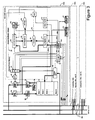
- Figure 1 shows an overall block diagram of a system which incorporates the memory card constructed according to the present invention.
- FIG. 2 shows in greater detail, the access control processor (ACP) of Figure 1 including a layout of its non-volatile memory.
- ACP access control processor
- Figure 3 shows a detailed block diagram of a standard flash memory of Figure 1 modified according to the present invention.
- FIGS 4 and 5 are flow charts used to explain the operation of the memory card of the present invention in carrying out various authentication procedures.
- FIG. 1 is a block diagram of a secure portable hand-held computing system usable as a personal computer or as a transaction processor.
- the system includes a memory card 3 constructed according to the present invention which connects to a host processor 5 by a bus 102.
- the host processor 5 may take the form of a palm top personal computer, such as the HP 95LX manufactured by Hewlett-Packard.
- the host processor 5 includes a liquid crystal display (LCD) 5-2, a keyboard 5-4, a microprocessor 5-6, a memory 5-8 and a serial interface 5-10 all coupled in common to a bus 106.
- the memory 5-8 includes a one megabyte read only memory (ROM) and a 512 Kbyte random access memory (RAM).
- bus 102 conforms to the Personal Computer Memory Card International Association (PCMCIA) standard.
- PCMCIA Personal Computer Memory Card International Association
- the interface 102 provides a path for transferring address, control and data information between host processor 5 and the memory card system 3 via a standard interface chip 104 and a memory card bus 105.
- Each of the buses 102, 105 and 106 include a data bus, a control bus and an address bus and provide continuous signal paths through all like buses.
- bus 105 includes address bus 105a, data bus 105b, and control bus 105c.
- the PCMCIA bus standard has evolved from a standard which supports disk emulation on memory cards to a substantially different standard which allows random access to memory data.
- the memory card of the present invention provides a protection technique which supports this new standard by providing rapid access to random memory locations without resort to encryption techniques. By controlling the data paths which carry the data from the memory array to the host, the memory card of the present invention protects the data without imposing any time-consuming buffering, decryption or other serial processing in this path.
- a user operates the system from the keyboard 5-4 to perform the typical operations such as spreadsheet and database functions which display information on display 5-2 and update information stored in files in memory card 3.
- the host processor 5 sends address information over bus 102 to retrieve information and if desired, updates the information and sends it, along with the necessary address and control information back to memory card 3.
- the memory card 3 of the present invention includes an access control processor (ACP) 10 coupled to bus 105 and a number (n) of CMOS flash memory chips 103a through 103n, each coupled to bus 105.
- ACP 10 is typically the same type of processing element as used in the "Smart Card”.
- the CMOS flash memories 103a through 103n may take the form of flash memory chips manufactured by Intel Corporation. For example, they make take the form of the Intel flash memory chip designated as Intel 28F001BX 1M which includes eight 128KBYTE x 8 CMOS flash memories.
- FIG. 2 shows in block diagram form, the access control processor (ACP) 10 of the preferred embodiment.
- ACP 10 includes a protected non-volatile memory 10-2, a random access memory (RAM) 10-4, a microprocessor 10-6, an interval counter 10-8 and an interface block 10-10 connected to bus 105.
- Non-volatile memory 10-2 dedicates a number of addressed locations in which to store authentication information and programs. More specifically, memory locations 10-2a store one or more personal identification numbers (PINs), protocol sequences or other identification information for verifying that the user has access to the system, and for identifying the blocks in flash memories 103a through 103n that the user may access in addition to a time interval value used for authentication.
- PINs personal identification numbers
- protocol sequences or other identification information
- Memory locations 10-2b store the key values used for protecting each of the flash memories 103a through 103n or the codes used to protect the individual blocks of each of the flash memories 103a through 103n.
- Memory locations 10-2c store the program instruction sequences for performing the required authentication operations and for clearing the system if the preset conditions for failure are met.
- Certain program instructions enable the user to control the setting of the interval counter 10-8 which establishes when user re-authentication takes place.
- the re-authentication interval defines the time between interruptions and for sending an interrupt to the host processor 5 requiring verification of the user's identity by having the user reenter the PIN or other password.
- the interval counter 10-8 receives clock pulses from the host processor 5 over bus 102 and can be set by the user according to the work environment. For example, at home, the user may turn the timer off (i.e., set it to a maximum value), or set the time interval to one hour. On an airplane the user may set it for ten minutes for increased protection. As described herein, the user is prompted to re-examine the setting of this interval at every "power on" thereby forcing periodic re-authentications to enforce security.
- FIG. 3 is a detailed block diagram of flash memories 103a through 103n. Only the detailed logic circuits of memory 103a are shown since memories 103b through 103n are constructed identically to memory 103a.
- the flash memory 103a basically comprises two sections, a section containing the security access control circuits of the present invention and another section containing the basic or standard logic circuits of the flash memory.
- the security control circuits of the present invention include a 32-bit key register, a 32-bit volatile lock register 33, a 12-bit delay counter 32, a comparator circuit 39, an all ONES detected signal circuit 38, a non-volatile lock memory 35, a one-bit non-volatile lock storage enable element 36, a volatile access control memory 43, an access modification allow AND gate 34 and an output OR gate 45 arranged as shown.
- this section receives command control signals designated by various hexadecimal values (e.g. 31H through 38H) from a command register 50 included in the basic logic section. These signals indicate the different data values of the set of commands received by the command register 50 from the ACP 10 via data bus 105b.
- the standard flash memory commands take the form of the commands utilized by the 28F001BX flash memory. Those commands are described in the publication entitled, "Memory Products,” published by Intel Corporation, referenced herein. The commands used by the present invention are described in Table 1.
- the first command shown is a load lock memory command which is used to initially load a random number generated lock value into non-volatile lock memory (LM) 35 in each memory 103a through 103n.
- LM non-volatile lock memory
- Each memory 103a through 103n may have a different lock value or the same lock value depending on the security needs of the users.
- the lock value is loaded into LM 35 through key (K) register 31 under control of the one bit, non-volatile storage element 36.
- K key
- the reset lock storage enable command of Table 1 is used to reset storage element 36. This prevents the lock value stored in LM 35 from being changed since storage element 36 once reset by the reset lock storage enable command cannot be set.
- the non-volatile contents of LM 35 are transferred to the L register 33 on power-up. It will be noted that the location or site of lock memory 35 is design dependent. For example, memory 35 could be implemented as an extension to memory array 54.
- the load key register command of Table 1 is used to load the key register 31 and set the delay counter 32.
- the decrement delay counter command is used by the ACP 10 to decrement by one, the contents of the delay counter 32.
- the read allow memory bank and read disable memory bank commands are used by the ACP 10 to enable or disable access to the different memory blocks of memory array 54 during loading of the access control memory 43.
- Load Key Register (32H) This command shifts the prior contents of the key register 31, one byte (LSB toward MSB) and loads "Key Value” from ACP 10 into the key register LSB. Further, it sets the Delay Counter 32 to its maximum value, e.g., all ONES. Decrement Delay Counter (35H) This command decrements the delay counter 32 by ONE. The delay counter must equal ZERO to allow subsequent reading of the memory array 54.
- Read-Allow Memory Bank (34H) This command sets the bit corresponding to the memory bank address (MBA) in the access control memory 43 if and only if the access modification allowed signal 37 is TRUE. This allows read access to the selected bank.
- Read-Disable Memory Bank (38H) This command resets the bit corresponding to the memory bank address in the access control memory 43.
- Table 1 also shows the bus cycle operations for each of the added commands.
- the command register 50 receives an 8-bit command generated by ACP 10, sent via the data bus 105a of bus 105 and an input buffer 51.
- Command register 50 conditions the selected logic element to receive from data bus 105b, the information required to execute the command during a second bus cycle.
- the second bus cycle is designated not applicable (N/A) since the reset lock storage enable and decrement delay counter commands need only one cycle for execution.
- the K register 31 is loaded with the key value received from memory locations 10-2b by a load key register command and delay counter 32 is set to its maximum value.
- Delay counter 32 is decremented to all ZEROS in response to successive decrement delay counter commands received from the ACP 10 and generates a zero count output signal 41 which is applied as an input to AND 34.
- Each delay counter 32 limits the number of tries or attempts which can be made to access the flash memories 103a through 103n in the case where a thief removes the chips and places them upon the "outlaw card" and programs a processor or equipment to repeatedly try to guess each memory chip's key. Stated differently, counter 32 ensures that a significant number of tries or attempts must be made in order to gain illegal access to the flash memories. The key and delay counter sizes are selected to require such testing to take an unreasonable amount of time.
- the Key Register 31 stores approximately 4 billion (2 32 ) different combinations.
- the delay counter 32 is a twelve-bit counter. Assuming the delay counter 32 is decremented once each microsecond, it will require 2 12 or 4 milliseconds per attempt at guessing the key value. The ACP 10, knowing the correct key value, incurs only a four millisecond delay in the initial setup. Random attempts to guess the key value will require 2 31 tries for a 50% chance of success. This would require 2 31 x 2 12 microseconds or 102 days to guess the key value. This time is sufficient to deter most thieves. Of course, a longer or shorter time could be provided by modifying the sizes of the key and delay counter 32.
- the ACP 10 limits the number of tries by the thief to guess the PIN by known techniques. Such techniques may include locking access or destroying data if a threshold of incorrect guesses is exceeded.
- a key value is loaded into the 32 bit K register 31 in response to four successive load key register commands (i.e., data bus 105b is a byte wide bus).
- Delay counter 32 is forced to its maximum count of (ALL ONE's) and decremented by the ACP 10 sending decrement delay counter commands on successive first bus cycles.
- the delay counter 32 is decremented to ZERO, it generates the zero count signal 41 which is applied to one input of AND gate 34.
- compare logic 39 applies an equals compare signal 42 to another input of AND gate 34. This causes AND gate 34 to generate an access modification allowed signal 37 at its output, which enables writing to access control memory 43, under the control of ACP 10. This, in turn, subsequently allows the reading of memory array 54.
- the access control memory 43 contains volatile storage of one bit for each block/bank of the memory array 54. These bits are cleared to ZERO as part of the flash memory's power up sequence. In order for data to be read from the memory 103a, the bit corresponding to the addressed memory block must be at logical ONE. These bits are set by the ACP 10 issuing read-allow memory bank commands if and only if the access modification allowed signal 37 is TRUE.
- the three (3) high order address bits of the selected memory bank of memory array 54 are sent over address bus 105c as well as a repeat of the hexadecimal command identifier being sent over the data bus 105a to command register 50. This results in a ONE being written into the addressed bit location in access control memory 43.
- the read-allow memory bank command sequence is repeated eight times since the memory array 54 is organized into eight banks of 16K bytes each.
- the ACP 10 may restrict access to selected banks by issuing a sequence of read-disable memory bank commands in a similar manner.
- the output of the access control memory 43 of the present invention is applied as an enabling input to output buffer 52 during each flash memory read cycle when the contents of a location of any bank of memory array 54 is being read out. That is, a read cycle may occur, however, the data read out is inhibited from passing through output buffer 52 in the absence of the appropriate bank's access control memory gating signal.
- access control memory 43 includes eight individually addressable bit storage elements, an input address 3 to 8-bit decoder connected to the input of each storage element and a 1 to 8 output multiplexer circuit connected to the output of each storage element. The three high order address bits of each address are decoded and used to select the storage element for the block whose contents are to be changed. Similarly, the same three bits are used to select the output of the storage element for the block containing the flash memory location being read.
- the output buffer 52 is always enabled. That is, when lock register 33 contains "ALL ONES," this generates a signal from ALL ONES detector element 38 to the OR gate 45 to enable the output buffer 52.
- such circuits include a memory array 54, a command register 50, input/output logic circuits 60, an address latch 56, a write state machine 61, erase voltage system 62, an output multiplexer 53, a data register 55, input buffer 51, output buffer 52 and a status register 58, as shown.
- the basic logic circuits of flash memory 103a takes the form of the type of circuits included in the flash memory designated as 28F001BX manufactured by Intel Corporation. Since such circuits are conventional, they will only be described to the extent necessary. For further information regarding such circuits, reference may be made to pages 3-109 through 3-134 of the publication entitled, "Memory Products," Order Number 210830, published by Intel Corporation, dated 1992.
- the flash memory basic circuits receive a number of input signals (A0-A16), address, data signals (D00-D07) and control signals (CE, WE, OE, PWD and VPP). These signals are described below in Table 2. Signal Descriptions Symbol Name and Function A0-A16 ADDRESS INPUTS for memory addresses. Addresses are internally latched during a write cycle. DOO-DO7 DATA INPUTS/OUTPUTS: Inputs data and commands during memory write cycles; outputs data during memory and status read cycles. The data pins are active high and float to tri-state off when the chip is deselected or the outputs are disabled. Data is internally latched during a write cycle.
- CE CHIP ENABLE Activates the device's control logic, input buffers, decoders and sense amplifiers.
- CE is active low, CE high deselects the memory device and reduces power consumption to standby levels.
- OE OUTPUT ENABLE Gates the device's outputs through the data buffers during a read cycle. OE is active low. WE WRITE ENABLE. Controls writes to the command register and array blocks. WE is active low. Addresses and data are latched on the rising edge of the WE pulse.
- Vpp ERASE/PROGRAM POWER SUPPLY for erasing blocks of the array or programming bytes of each block. Note: With Vpp ⁇ Vppl Max, memory contents cannot be altered.
- the Chip Enable (CE), Write Enable processor (WE) and Output Enable (OE)) signals are applied to command register 50 and I/O logic 60 from host processor 5, via bus 102 and control bus 105b and are dispersed to control specified logic blocks.
- a powerdown (PWD) signal is also applied to command register 50 for enabling the flash memory to perform the operations specified in Table 2. This signal can be used to clear the volatile storage elements of the flash memory's security control section as desired thereby enforcing user reauthentication when normal operation is again resumed.
- the basic logic elements of the flash memory operate in the following manner.
- Information is stored in memory array 54 via data bus 105a, input buffer 51 and data register 55 at an addressed location of one of the memory blocks specified by the address received by an address logic 56 from address bus 105c.
- Information is read from a specified address location of a bank of memory array 54 and is sent to host processor 5 via an output multiplexer 53, output buffer 52, data bus 105a and bus 102.
- Status register 58 is used for storing the status of the write state machine, the error suspend status, the erase status, the program status and the Vpp status.
- the write state machine 61 controls the block erase and controls program algorithms.
- the program/erase voltage system 62 is used for erasing blocks of the memory array 54 or the programming bytes of each block as a function of the level of Vpp (i.e., when Vpp is at a high level programming can take place; if Vpp is at a low level, memory array 54 functions as a read only memory).
- the ACP 10 sets the lock value for each of the memory chips on the memory card. It does this by loading the key value into the lock memory of Figure 3. These values are stored in the ACP's protected non-volatile memory 10-2 (i.e., keys 1-n in Figure 2).
- the lock storage enable elements 36 are then set to ZEROs to inhibit further changing or reading of lock memory contents. As these elements are nonvolatile, they cannot be changed unless the entire flash memory chip is cleared.
- the memory card can then be loaded with its data or software application.
- the ACP 10 is then loaded with information pertaining to the memory's bank structure and the degrees of protection which are to be applied to each memory bank.
- the user establishes parameters for the frequency and mode of authentication and specific data required (e.g., personal identification numbers (PINs)). This information is stored in the ACP's memory.
- PINs personal identification numbers
- the "key register”, "access modification allowed” signal and "access control memory” are initialized so as to inhibit access to data or writing to access control memory 43.
- the first authentication dialog is initiated.
- the ACP 10 using the services of its host processor 5, prompts the user and receives authentication information. If authentication is unsuccessful, no operation is performed; if successful, the key register of each memory chip is loaded with the value stored in the ACP's memory. During this operation, the delay counter 32 is used to inhibit chip operation for a period of time following loading to make random tries an unproductive process. Loading of the key registers causes the "access modification allowed" signal to be true in each chip. The ACP 10 then establishes access by loading the access control memories according to the stored information configuration
- the ACP 10 prompts an additional user authentication (reauthentication).
- the ACP 10 forces all memory chips to their power on states, thus inhibiting any access to the memories' data by clearing the access control memory 43 and clearing the contents of the key register 31.
- FIG. 4 shows in block diagram form, the various modes of operation.
- Blocks 402 and 401 show the two startup conditions.
- the user inserts the memory card 3 in the previously powered-up host processor 5.
- the user powers up host processor 5 with memory card 3 already installed.
- block 403 clears all of the 'n' K registers 31 and the 'n' access control memories 43 as part of the flash memories 103a through 103n internal initialization sequence. This prevents any data from being read out of memories 103a through 103n since output buffer 52, in each memory, is disabled.
- the lock value is loaded into the 'n' L registers 33 from the respective LMs 35 as a result of power on.
- ACP 10 sends an interrupt signal to host processor 5 which responds by requesting the PIN or other identifying information from the user.
- ACP 10 by means of the program stored in memory locations 10-2a, checks that the PIN or other identifying information matches the information stored in memory locations 10-2a. If no match, then decision block 406 counts an error and ACP 10 branches to block 404 to repeat the test. If the test fails a preset number of times, then decision block 406 branches to block 407 to cause ACP 10 to either lock up or destroy the contents of the memories 103a through 103n.
- block 408 the ACP 10 via a load key register command loads each K register 31 from memory locations 10-2b with the appropriate key value. Also block 409 repeatedly decrements the contents of delay counter 32 issuing successive the decrement delay counter commands toward a binary zero count which causes the generation of the zero count signal.
- each access control memory 43 location is loaded with information by means of the read-allow memory bank command to allow access to the selected banks of the corresponding flash memory 103a through 103n.
- the ACP 10 awaits the end of the preset time interval established by information stored in memory locations 10-2a signalled by interval counter 10-8 before requesting user re-authentication. Then, in block 412, the ACP 10 interrupts the host processor 5 to request the user to re-enter the PIN or other required identification.
- Decision block 413 checks the PIN or other information received from the host processor 5 against the information stored in memory locations 10-2a and the interval timer 10-8 output is recorded. The user has a preset time interval of typically 30 seconds in which to enter the authentication information into host processor 5. While the clock is running, if the decision block 413 test fails, then block 414 records the test as an error. At that time, it checks if a maximum number of errors was received and branches to repeat blocks 412 and 413. If the number of errors equals the maximum number, then in block 415, APC 10 clears the flash memory K register 31 by means of successive load key register commands, and clears the access control memories 43 with successive read-disable memory commands. Block 415 then branches to block 404 to allow a new "First Authentication" operation to take place.
- the K register 31 remains unchanged (i.e., contains the key value previously loaded by the ACP) enabling the user to continue to operate the system 1.
- the ACP 10 clears the K register 31 and the access control memory 43 as before.
- Figure 5 is a flow diagram which illustrates how host processor 5 responds to an interrupt request from APC 10 for authentication in response to blocks 404 and 412 of Figure 4.
- decision block 501 is waiting for an interrupt from the ACP 10 requesting that the user re-enter the PIN or other information.
- Decision block 501 branches to block 502 when it receives the interrupt from blocks 404 or 412.
- Block 502 displays the request for the PIN or other information on host display 5-2.
- Block 503 accepts the information from the keyboard and block 504 interrupts ACP 10.
- Block 5 sends the PIN to ACP 10.
Abstract
Description
- This invention relates to the field of portable personal computers and more particularly to maintaining systems for data security in a portable digital information environment.
- The security of personal information has forever been a concern. It has been ensured by locks, codes and secret pockets. As information has taken new forms, new methods have been required to meet the changed situations.
- Historically, security of information has been addressed by use of signatures, credentials and photographs. Electronic devices such as automatic banking machines have added encoded cards and personal identification numbers (PINs) to the repertoire of security tools. Computer systems continue to use passwords.
- More recently the "Smart Card" has been used as a security tool. The "Smart Card" is a small microcomputer with writable, non-volatile memory and a simple input/output interface, fabricated as a single chip and embedded in a plastic "credit card". It has exterior pads to allow it to be connected to specially designed equipment. The program contained in the card's microcomputer interacts with this equipment and allows its nonvolatile memory data to be read or modified according to the desired algorithm which may optionally include a password exchange. Special techniques have been implemented to protect the memory information and to allow varied permissions according to the situation. For example, U.S. Patent No. 4,382,279 entitled, "Single Chip Microprocessor with On-Chip Modifiable Memory" discloses an architecture which permits automatic programming of a non-volatile memory which is included on the same chip as a processing and control unit. As in other systems, the microprocessor only protects memory on the same chip.
- The "Smart Card" has been used both to facilitate the process of identification and to be the actual site of the valued information. In this situation, as in most past situations, physical presence of a "key" as well as some special knowledge has been used as part of the verification or authentication process. In such above cases, identification has been a dialog between the person desiring access and a fixed agency such as a security guard or an automatic teller machine.
- The current state of portability of freestanding computing devices makes it possible for both the physical key and the authentication agent to be small, portable and hence more subject to loss or theft. Further, computing devices make it possible to perform repeated attempts to guess or deduce the special knowledge or password associated with the identification process. This is especially true if the authentication agent or device is also in the control of the thief or burglar. To make matters worse, technology now allows and encourages the carrying of enormous amounts of sensitive information in a pocket or handbag where it is subject to mishap.
- Today, notebook and subnotebook sized computers provide a capable freestanding environment which allows for significant computing power and thus creates a need for additional data storage capability. This has initially been met by miniature hard disk devices which hold both programs and data. While password protection is often used in these systems, it does not completely protect sensitive data because, first, the authentication agent is itself vulnerable. However, more significantly, the disk drive containing the data can be physically removed and accessed in a setting more conducive to data analysis. In this case, only some form of encryption is capable of protecting the data. The nature of disk access makes this possible without undue performance or cost barriers. An example of this type of system is described in U.S. Patent No. 4,985,920 entitled, "Integrated Circuit Card."
- The recent emergence of the flash memory and removable "memory cards" has allowed major reductions in size and power requirements of the portable computer. The flash memory combines the flexibility of random access memory (RAM) with the permanence of disks. Today, the coupling of these technologies allows up to 20 million bytes of data to be contained, without need of power, in a credit card size, removable package. This data can be made to appear to a host system either as if it were contained in a conventional disk drive or as if it were an extension of the host's memory. These technological developments have made further reduction in system size possible to the extent that it may be carried in a pocket rather than in a handbag or briefcase.
- Thus, the data and its host system have become more vulnerable to loss or theft and simultaneously more difficult to protect memory data by encryption as this presents major cost and performance barriers. Document EP-A-0 212 615 concerns a memory card including deciphering means 57. Moreover, it includes means for securing the memory 65 (
system controller 56, code comparator 63, address comparator 68) but these means are external to the memory 65, so that the document cannot teach memory 65 as a memory chip which would be secured by internal securing means if removed from the card. - Accordingly, it is a primary object of the invention to provide a portable digital system with a secure memory subsystem.
- It is another object of the invention to provide a memory card which can be protected if removed from a portable digital system.
- It is still a further object of the present invention to provide a memory card in which the chips of the card are protected if removed from such card.
- The above objects are achieved in a secure memory card according to
claim 1. The secure memory card includes a microprocessor on a single semiconductor chip and one or more non-volatile addressable memory chips. The microprocessor chip and nonvolatile memory chips connect in common to an internal card bus for transmitting address, data and control information to such non-volatile memory chips. The microprocessor includes an addressable non-volatile memory for storing information including a number of key values, configuration information and program instruction information for controlling the transfer of address, data and control information on the internal bus. The chip memory is organized into a number of blocks or banks, each block having a plurality of addressable locations. - According to the present invention, each memory chip is constructed to include security control logic circuits. In the preferred embodiment, these circuits include a non-volatile lock memory, a non-volatile lock storage enable element and a volatile access control memory, each being loadable under the control of the microprocessor. More specifically, the microprocessor first loads a lock value into the non-volatile lock memory and resets the lock storage enable element inhibiting access. Thereafter, the microprocessor loads the access control memory as specified by the configuration information. Such information is loaded only after the microprocessor has determined that the user has successfully performed a predetermined authentication procedure with a host computer. The security logic circuits of each memory enable the reading of information stored in selected addressed blocks of the flash memory as a function of the configuration information loaded into the memory chip's access control memory. Periodically, the user is required to successfully perform an authentication procedure with the host computer, and the user is allowed to continue reading information as allowed by the access control memory. In the preferred embodiment, the host computer is coupled to the memory card through a standard interface such as the interface which conforms to the Personal Computer Memory Card International Association (PCMCIA) standards.
- The present invention melts the "SmartCard" and "memory card" technologies which is key to allowing the protection of the large amounts of data made possible by the flash memory technology in the "security harsh" environments which electronic miniaturization has created. Further, the present invention is able to take advantage of improvements and enhancements in both technologies.
- Additionally, the security logic circuits of the present invention are incorporated into and operate in conjunction with the flash memory in a way that minimizes the amount of changes required to be made to the basic logic circuits of the flash memory. More specifically, the flash memory can be operated in a secure mode and in a non-secure mode wherein the security logic circuits are bypassed enabling the flash memory to operate as if such circuits had not been installed. The non-secure mode is normally entered when the contents of the flash memory's non-volatile lock memory are cleared. This is generally indicative of an unprogrammed or fully erased flash memory which naturally erases to a predetermined state (i.e. an all ONES state).
- With the addition of a small amount of logic to the flash memory and an "Access Control Processor" (ACP), the contents of the flash memory is made secure without requiring data encryption. Therefore, the invention eliminates the overhead of encrypting and decrypting data which can be quite time-consuming for large blocks of data.
- In operation, the ACP periodically prompts the user of the system for entry of some form of authentication. This may be a password, a PIN, a specific pen computer "gesture" performed at a specific point on the writing surface, a spoken command or a "voiceprint" of the user. The method varies with the system. The programmable ACP allows the user to alter the specific content of the authentication and the frequency of prompting. The code for authentication and the data required by the lock and access control memories are stored within the ACP's non-volatile memory which is on the same chip as the ACP and, hence, are protected.
- As mentioned, a successful authentification causes the ACP to enable, or continue to enable, all or selected blocks of the flash memory for access. Failure causes access to the flash memory to be disabled. Thus, the operation is similar to a "dead man throttle" in that any failure to successfully complete authentication will cause the flash memory's data to be protected. In addition, a command initiated by the user can also cause access to be disabled. Further, upon first application of power from a powered off condition, access is blocked to protected memory contents until the first authentication is successfully performed.
- Thus, if either the memory card or its host processor is lost, stolen, powered off or left unattended, the memory's data is protected from access, either immediately or as soon as the current periodic authentication expires. In the event of theft, the memory data is protected from access even if the memory card is opened and probed electronically or the memory chips are removed and placed in another device.
- The above objects and advantages of the present invention will be better understood from the following description when taken in conjunction with the accompanying drawings.
- Figure 1 shows an overall block diagram of a system which incorporates the memory card constructed according to the present invention.
- Figure 2 shows in greater detail, the access control processor (ACP) of Figure 1 including a layout of its non-volatile memory.
- Figure 3 shows a detailed block diagram of a standard flash memory of Figure 1 modified according to the present invention.
- Figures 4 and 5 are flow charts used to explain the operation of the memory card of the present invention in carrying out various authentication procedures.
- Figure 1 is a block diagram of a secure portable hand-held computing system usable as a personal computer or as a transaction processor. The system includes a
memory card 3 constructed according to the present invention which connects to ahost processor 5 by abus 102. Thehost processor 5 may take the form of a palm top personal computer, such as the HP 95LX manufactured by Hewlett-Packard. Thehost processor 5 includes a liquid crystal display (LCD) 5-2, a keyboard 5-4, a microprocessor 5-6, a memory 5-8 and a serial interface 5-10 all coupled in common to abus 106. The memory 5-8 includes a one megabyte read only memory (ROM) and a 512 Kbyte random access memory (RAM). - The connection between the
memory card 3 andhost processor 5 is established through a standard bus interface. In the preferred embodiment, thebus 102 conforms to the Personal Computer Memory Card International Association (PCMCIA) standard. Theinterface 102 provides a path for transferring address, control and data information betweenhost processor 5 and thememory card system 3 via astandard interface chip 104 and amemory card bus 105. Each of thebuses bus 105 includesaddress bus 105a,data bus 105b, andcontrol bus 105c. - The PCMCIA bus standard has evolved from a standard which supports disk emulation on memory cards to a substantially different standard which allows random access to memory data. The memory card of the present invention provides a protection technique which supports this new standard by providing rapid access to random memory locations without resort to encryption techniques. By controlling the data paths which carry the data from the memory array to the host, the memory card of the present invention protects the data without imposing any time-consuming buffering, decryption or other serial processing in this path.
- Typically, a user operates the system from the keyboard 5-4 to perform the typical operations such as spreadsheet and database functions which display information on display 5-2 and update information stored in files in
memory card 3. Thehost processor 5 sends address information overbus 102 to retrieve information and if desired, updates the information and sends it, along with the necessary address and control information back tomemory card 3. - As shown in Figure 1, the
memory card 3 of the present invention includes an access control processor (ACP) 10 coupled tobus 105 and a number (n) of CMOSflash memory chips 103a through 103n, each coupled tobus 105.ACP 10 is typically the same type of processing element as used in the "Smart Card". TheCMOS flash memories 103a through 103n may take the form of flash memory chips manufactured by Intel Corporation. For example, they make take the form of the Intel flash memory chip designated as Intel 28F001BX 1M which includes eight 128KBYTE x 8 CMOS flash memories. Thus, a 4-MBYTE flash memory card could include 32 - CMOS flash memories, that is 'n' = 32. - Figure 2 shows in block diagram form, the access control processor (ACP) 10 of the preferred embodiment. As shown,
ACP 10 includes a protected non-volatile memory 10-2, a random access memory (RAM) 10-4, a microprocessor 10-6, an interval counter 10-8 and an interface block 10-10 connected tobus 105. Non-volatile memory 10-2 dedicates a number of addressed locations in which to store authentication information and programs. More specifically, memory locations 10-2a store one or more personal identification numbers (PINs), protocol sequences or other identification information for verifying that the user has access to the system, and for identifying the blocks inflash memories 103a through 103n that the user may access in addition to a time interval value used for authentication. - Memory locations 10-2b store the key values used for protecting each of the
flash memories 103a through 103n or the codes used to protect the individual blocks of each of theflash memories 103a through 103n. - Memory locations 10-2c store the program instruction sequences for performing the required authentication operations and for clearing the system if the preset conditions for failure are met. Certain program instructions enable the user to control the setting of the interval counter 10-8 which establishes when user re-authentication takes place. The re-authentication interval defines the time between interruptions and for sending an interrupt to the
host processor 5 requiring verification of the user's identity by having the user reenter the PIN or other password. The interval counter 10-8 receives clock pulses from thehost processor 5 overbus 102 and can be set by the user according to the work environment. For example, at home, the user may turn the timer off (i.e., set it to a maximum value), or set the time interval to one hour. On an airplane the user may set it for ten minutes for increased protection. As described herein, the user is prompted to re-examine the setting of this interval at every "power on" thereby forcing periodic re-authentications to enforce security. - Figure 3 is a detailed block diagram of
flash memories 103a through 103n. Only the detailed logic circuits ofmemory 103a are shown sincememories 103b through 103n are constructed identically tomemory 103a. - The
flash memory 103a basically comprises two sections, a section containing the security access control circuits of the present invention and another section containing the basic or standard logic circuits of the flash memory. - As seen from Figure 3, the security control circuits of the present invention include a 32-bit key register, a 32-bit volatile lock register 33, a 12-
bit delay counter 32, acomparator circuit 39, an all ONES detected signal circuit 38, anon-volatile lock memory 35, a one-bit non-volatile lock storage enableelement 36, a volatileaccess control memory 43, an access modification allow ANDgate 34 and an output OR gate 45 arranged as shown. It will be noted that this section receives command control signals designated by various hexadecimal values (e.g. 31H through 38H) from acommand register 50 included in the basic logic section. These signals indicate the different data values of the set of commands received by thecommand register 50 from theACP 10 viadata bus 105b. These commands are an important extension to the sets of commands normally used by the flash memory. The standard flash memory commands take the form of the commands utilized by the 28F001BX flash memory. Those commands are described in the publication entitled, "Memory Products," published by Intel Corporation, referenced herein. The commands used by the present invention are described in Table 1. - Referring to Table 1, the first command shown is a load lock memory command which is used to initially load a random number generated lock value into non-volatile lock memory (LM) 35 in each
memory 103a through 103n. Eachmemory 103a through 103n may have a different lock value or the same lock value depending on the security needs of the users. The lock value is loaded intoLM 35 through key (K) register 31 under control of the one bit,non-volatile storage element 36. The reset lock storage enable command of Table 1 is used to resetstorage element 36. This prevents the lock value stored inLM 35 from being changed sincestorage element 36 once reset by the reset lock storage enable command cannot be set. The non-volatile contents ofLM 35 are transferred to the L register 33 on power-up. It will be noted that the location or site oflock memory 35 is design dependent. For example,memory 35 could be implemented as an extension to memory array 54. - The load key register command of Table 1 is used to load the
key register 31 and set thedelay counter 32. The decrement delay counter command is used by theACP 10 to decrement by one, the contents of thedelay counter 32. The read allow memory bank and read disable memory bank commands are used by theACP 10 to enable or disable access to the different memory blocks of memory array 54 during loading of theaccess control memory 43.Command First Bus Cycle Operation Address Data Second Bus Cycle Operation Address Data Load Lock Memory Write 31H Write N/A Reset Lock Storage Enable Write 33H N/A N/A Load Key Register Write 32H Write Key Data Decrement Delay Counter Write 35H N/A N/A Read-Allow Memory Bank Write MBA 34H Write MBA Read-Disable Memory Bank Write MBA 38H Write MBA Load Lock Memory (31H)
This command copies the contents of thekey register 31 into thenon-volatile lock memory 35 if and only if the lock storage enable 36 output signal is TRUE.Reset Lock Storage Enable (33H)
This command resets the lock storage enablelogic element 36, thus inhibiting loading or changing thelock storage memory 35.Load Key Register (32H)
This command shifts the prior contents of thekey register 31, one byte (LSB toward MSB) and loads "Key Value" fromACP 10 into the key register LSB. Further, it sets theDelay Counter 32 to its maximum value, e.g., all ONES.Decrement Delay Counter (35H)
This command decrements thedelay counter 32 by ONE. The delay counter must equal ZERO to allow subsequent reading of the memory array 54.Read-Allow Memory Bank (34H)
This command sets the bit corresponding to the memory bank address (MBA) in theaccess control memory 43 if and only if the access modification allowedsignal 37 is TRUE. This allows read access to the selected bank.Read-Disable Memory Bank (38H)
This command resets the bit corresponding to the memory bank address in theaccess control memory 43. - Considering Table 1 in greater detail, it is seen that Table 1 also shows the bus cycle operations for each of the added commands. For each command requiring two bus cycles, during each first bus cycle, the
command register 50 receives an 8-bit command generated byACP 10, sent via thedata bus 105a ofbus 105 and aninput buffer 51.Command register 50 conditions the selected logic element to receive fromdata bus 105b, the information required to execute the command during a second bus cycle. As indicated, the second bus cycle is designated not applicable (N/A) since the reset lock storage enable and decrement delay counter commands need only one cycle for execution. - During normal operation, the
K register 31 is loaded with the key value received from memory locations 10-2b by a load key register command and delaycounter 32 is set to its maximum value. Delaycounter 32 is decremented to all ZEROS in response to successive decrement delay counter commands received from theACP 10 and generates a zero count output signal 41 which is applied as an input to AND 34. - Each
delay counter 32 limits the number of tries or attempts which can be made to access theflash memories 103a through 103n in the case where a thief removes the chips and places them upon the "outlaw card" and programs a processor or equipment to repeatedly try to guess each memory chip's key. Stated differently, counter 32 ensures that a significant number of tries or attempts must be made in order to gain illegal access to the flash memories. The key and delay counter sizes are selected to require such testing to take an unreasonable amount of time. - More specifically, the
Key Register 31 stores approximately 4 billion (232) different combinations. In the preferred embodiment, thedelay counter 32 is a twelve-bit counter. Assuming thedelay counter 32 is decremented once each microsecond, it will require 212 or 4 milliseconds per attempt at guessing the key value. TheACP 10, knowing the correct key value, incurs only a four millisecond delay in the initial setup. Random attempts to guess the key value will require 231 tries for a 50% chance of success. This would require 231 x 212 microseconds or 102 days to guess the key value. This time is sufficient to deter most thieves. Of course, a longer or shorter time could be provided by modifying the sizes of the key and delaycounter 32. - In the case where the memory card of the present invention is stolen and is put into an "outlaw host," the
ACP 10 limits the number of tries by the thief to guess the PIN by known techniques. Such techniques may include locking access or destroying data if a threshold of incorrect guesses is exceeded. - During an initial authentication operation for
flash memory 103a, a key value is loaded into the 32 bit Kregister 31 in response to four successive load key register commands (i.e.,data bus 105b is a byte wide bus). Delaycounter 32 is forced to its maximum count of (ALL ONE's) and decremented by theACP 10 sending decrement delay counter commands on successive first bus cycles. When thedelay counter 32 is decremented to ZERO, it generates the zero count signal 41 which is applied to one input of ANDgate 34. - If the key value stored in the
K register 31 equals the lock value stored in the corresponding L register 33 indicating that the user provided the proper identification to thehost processor 5, then comparelogic 39 applies an equals comparesignal 42 to another input of ANDgate 34. This causes ANDgate 34 to generate an access modification allowedsignal 37 at its output, which enables writing to accesscontrol memory 43, under the control ofACP 10. This, in turn, subsequently allows the reading of memory array 54. - The
access control memory 43 contains volatile storage of one bit for each block/bank of the memory array 54. These bits are cleared to ZERO as part of the flash memory's power up sequence. In order for data to be read from thememory 103a, the bit corresponding to the addressed memory block must be at logical ONE. These bits are set by theACP 10 issuing read-allow memory bank commands if and only if the access modification allowedsignal 37 is TRUE. - As shown in Table 1, during the second bus cycle of the read-allow memory bank command, the three (3) high order address bits of the selected memory bank of memory array 54 are sent over
address bus 105c as well as a repeat of the hexadecimal command identifier being sent over thedata bus 105a to commandregister 50. This results in a ONE being written into the addressed bit location inaccess control memory 43. In the preferred embodiment, the read-allow memory bank command sequence is repeated eight times since the memory array 54 is organized into eight banks of 16K bytes each. TheACP 10 may restrict access to selected banks by issuing a sequence of read-disable memory bank commands in a similar manner. - The output of the
access control memory 43 of the present invention is applied as an enabling input tooutput buffer 52 during each flash memory read cycle when the contents of a location of any bank of memory array 54 is being read out. That is, a read cycle may occur, however, the data read out is inhibited from passing throughoutput buffer 52 in the absence of the appropriate bank's access control memory gating signal. More specifically, in the case of the preferred embodiment,access control memory 43 includes eight individually addressable bit storage elements, aninput address 3 to 8-bit decoder connected to the input of each storage element and a 1 to 8 output multiplexer circuit connected to the output of each storage element. The three high order address bits of each address are decoded and used to select the storage element for the block whose contents are to be changed. Similarly, the same three bits are used to select the output of the storage element for the block containing the flash memory location being read. - If the
lock memory 35 is fully erased, i.e., at ALL ONES as indicated by the contents of the L register 33 being at all ONES, then theoutput buffer 52 is always enabled. That is, when lock register 33 contains "ALL ONES," this generates a signal from ALL ONES detector element 38 to the OR gate 45 to enable theoutput buffer 52. This effectively placesflash memory 103a in non-secure mode. This allows all of the security logic circuits of the present invention to be bypassed. Hence, the same flash memory chip can be used for both secure and non-secure applications, thus resulting in production economies. - As shown in Figure 3, such circuits include a memory array 54, a
command register 50, input/output logic circuits 60, anaddress latch 56, a write state machine 61, erasevoltage system 62, an output multiplexer 53, a data register 55,input buffer 51,output buffer 52 and a status register 58, as shown. The basic logic circuits offlash memory 103a as discussed above, takes the form of the type of circuits included in the flash memory designated as 28F001BX manufactured by Intel Corporation. Since such circuits are conventional, they will only be described to the extent necessary. For further information regarding such circuits, reference may be made to pages 3-109 through 3-134 of the publication entitled, "Memory Products," Order Number 210830, published by Intel Corporation, dated 1992. As shown in Figure 3, the flash memory basic circuits receive a number of input signals (A0-A16), address, data signals (D00-D07) and control signals (CE, WE, OE, PWD and VPP). These signals are described below in Table 2.Signal Descriptions Symbol Name and Function A0-A16 ADDRESS INPUTS for memory addresses. Addresses are internally latched during a write cycle. DOO-DO7 DATA INPUTS/OUTPUTS: Inputs data and commands during memory write cycles; outputs data during memory and status read cycles. The data pins are active high and float to tri-state off when the chip is deselected or the outputs are disabled. Data is internally latched during a write cycle. CE CHIP ENABLE: Activates the device's control logic, input buffers, decoders and sense amplifiers. CE is active low, CE high deselects the memory device and reduces power consumption to standby levels. PWD POWERDOWN: Puts the device in deep powerdown mode. PWD s active low; PWD high gates normal operation. PWD=VHH allows programming of the memory blocks. PWD also locks out erase or write operations when active low, providing data protection during power transitions. OE OUTPUT ENABLE: Gates the device's outputs through the data buffers during a read cycle. OE is active low. WE WRITE ENABLE. Controls writes to the command register and array blocks. WE is active low. Addresses and data are latched on the rising edge of the WE pulse. Vpp ERASE/PROGRAM POWER SUPPLY for erasing blocks of the array or programming bytes of each block. Note: With Vpp < Vppl Max, memory contents cannot be altered. - As shown in Table 2, the Chip Enable (CE), Write Enable processor (WE) and Output Enable (OE)) signals are applied to
command register 50 and I/O logic 60 fromhost processor 5, viabus 102 andcontrol bus 105b and are dispersed to control specified logic blocks. A powerdown (PWD) signal is also applied to command register 50 for enabling the flash memory to perform the operations specified in Table 2. This signal can be used to clear the volatile storage elements of the flash memory's security control section as desired thereby enforcing user reauthentication when normal operation is again resumed. - Generally, the basic logic elements of the flash memory operate in the following manner. Information is stored in memory array 54 via
data bus 105a,input buffer 51 and data register 55 at an addressed location of one of the memory blocks specified by the address received by anaddress logic 56 fromaddress bus 105c. Information is read from a specified address location of a bank of memory array 54 and is sent to hostprocessor 5 via an output multiplexer 53,output buffer 52,data bus 105a andbus 102. Status register 58 is used for storing the status of the write state machine, the error suspend status, the erase status, the program status and the Vpp status. - The write state machine 61 controls the block erase and controls program algorithms. The program/erase
voltage system 62 is used for erasing blocks of the memory array 54 or the programming bytes of each block as a function of the level of Vpp (i.e., when Vpp is at a high level programming can take place; if Vpp is at a low level, memory array 54 functions as a read only memory). - The operation of the secure memory card of the present invention will now be described with particular reference to the flow diagram of Figures 4 and 5. Before describing such operations in detail, the steps involved in the fabrication, customization and operation of the memory card will first be described.
- As a first step, at card fabrication, the
ACP 10 sets the lock value for each of the memory chips on the memory card. It does this by loading the key value into the lock memory of Figure 3. These values are stored in the ACP's protected non-volatile memory 10-2 (i.e., keys 1-n in Figure 2). The lock storage enableelements 36 are then set to ZEROs to inhibit further changing or reading of lock memory contents. As these elements are nonvolatile, they cannot be changed unless the entire flash memory chip is cleared. - As a second step, at application customization, since writing is not affected by the protection functionality, the memory card can then be loaded with its data or software application. The
ACP 10 is then loaded with information pertaining to the memory's bank structure and the degrees of protection which are to be applied to each memory bank. - As a third step, at user customization, the user establishes parameters for the frequency and mode of authentication and specific data required (e.g., personal identification numbers (PINs)). This information is stored in the ACP's memory.
- As a fourth step, at power on, the "key register", "access modification allowed" signal and "access control memory" are initialized so as to inhibit access to data or writing to access
control memory 43. The first authentication dialog is initiated. - At first authentication dialog, the
ACP 10, using the services of itshost processor 5, prompts the user and receives authentication information. If authentication is unsuccessful, no operation is performed; if successful, the key register of each memory chip is loaded with the value stored in the ACP's memory. During this operation, thedelay counter 32 is used to inhibit chip operation for a period of time following loading to make random tries an unproductive process. Loading of the key registers causes the "access modification allowed" signal to be true in each chip. TheACP 10 then establishes access by loading the access control memories according to the stored information configuration - As a sixth step, at subsequent authentication dialog, periodically, according to the user's configuration, the
ACP 10 prompts an additional user authentication (reauthentication). In the event of failure, theACP 10 forces all memory chips to their power on states, thus inhibiting any access to the memories' data by clearing theaccess control memory 43 and clearing the contents of thekey register 31. Now, the operation of the system of Figure 1 will be described with reference to Figures 4 and 5. - Figure 4 shows in block diagram form, the various modes of operation.
Blocks 402 and 401 show the two startup conditions. In block 402, the user inserts thememory card 3 in the previously powered-uphost processor 5. Inblock 401, the user powers uphost processor 5 withmemory card 3 already installed. - In either of the above startup operations, during
block 402b, theACP 10 and its interfaces are initialized in a conventional manner, and block 403 clears all of the 'n' K registers 31 and the 'n'access control memories 43 as part of theflash memories 103a through 103n internal initialization sequence. This prevents any data from being read out ofmemories 103a through 103n sinceoutput buffer 52, in each memory, is disabled. The lock value is loaded into the 'n' L registers 33 from therespective LMs 35 as a result of power on. - Now in
block 404,ACP 10 sends an interrupt signal to hostprocessor 5 which responds by requesting the PIN or other identifying information from the user. In block 405,ACP 10, by means of the program stored in memory locations 10-2a, checks that the PIN or other identifying information matches the information stored in memory locations 10-2a. If no match, then decision block 406 counts an error andACP 10 branches to block 404 to repeat the test. If the test fails a preset number of times, then decision block 406 branches to block 407 to causeACP 10 to either lock up or destroy the contents of thememories 103a through 103n. - If in decision block 405 there is a match indicating a successful authentication then in
block 408, theACP 10 via a load key register command loads each K register 31 from memory locations 10-2b with the appropriate key value. Also block 409 repeatedly decrements the contents ofdelay counter 32 issuing successive the decrement delay counter commands toward a binary zero count which causes the generation of the zero count signal. - In
block 410, eachaccess control memory 43 location is loaded with information by means of the read-allow memory bank command to allow access to the selected banks of thecorresponding flash memory 103a through 103n. - In block 411, the
ACP 10 awaits the end of the preset time interval established by information stored in memory locations 10-2a signalled by interval counter 10-8 before requesting user re-authentication. Then, inblock 412, theACP 10 interrupts thehost processor 5 to request the user to re-enter the PIN or other required identification. -
Decision block 413 checks the PIN or other information received from thehost processor 5 against the information stored in memory locations 10-2a and the interval timer 10-8 output is recorded. The user has a preset time interval of typically 30 seconds in which to enter the authentication information intohost processor 5. While the clock is running, if thedecision block 413 test fails, then block 414 records the test as an error. At that time, it checks if a maximum number of errors was received and branches to repeatblocks block 415,APC 10 clears the flashmemory K register 31 by means of successive load key register commands, and clears theaccess control memories 43 with successive read-disable memory commands.Block 415 then branches to block 404 to allow a new "First Authentication" operation to take place. - If the test in
decision block 413 is successful, theK register 31 remains unchanged (i.e., contains the key value previously loaded by the ACP) enabling the user to continue to operate thesystem 1. In the event that the 30 seconds elapsed withoutdecision block 413 receiving the PIN or other information, theACP 10 clears theK register 31 and theaccess control memory 43 as before. - Figure 5 is a flow diagram which illustrates how
host processor 5 responds to an interrupt request fromAPC 10 for authentication in response toblocks decision block 501 is waiting for an interrupt from theACP 10 requesting that the user re-enter the PIN or other information. Decision block 501 branches to block 502 when it receives the interrupt fromblocks Block 503 accepts the information from the keyboard and block 504 interruptsACP 10.Block 5 sends the PIN toACP 10. - It will be appreciated by those skilled in the art that many changes may be made to the preferred embodiment of the present invention without departing from its teachings. For example, the invention may be used with different types of non-volatile memories and different interfaces, etc.
- While in accordance with the provisions and statutes there has been illustrated and described the best form of the invention, certain changes may be made without departing from the invention as set forth in the appended claims.
Claims (20)
- A secure memory card for use with a host portable computer, said memory card comprising:a microprocessor (10-6) connected for transmitting and receiving address, data and control information to and from said host computer (5) and including a first addressable non-volatile memory (10-2) for storing information including a number of key values and configuration information;an internal bus (105) connected to said microprocessor for transmitting address, data and control information defining memory operations to be performed by said card ; and,a set of second addressable non-volatile memories including at least one second non-volatile memory (103a) connected to said internal bus in common with said microprocessor for receiving said address, data and control information, said memory including a non volatile memory section and a security control section, said memory section containing on the one hand a memory array (54) organized into a number of blocks, each block having a plurality of addressable locations, and on the other hand control logic means (50) for performing said memory operations and said security control section being connected to said internal bus, to said control logic means and to said memory array, said security control section including:a number of non-volatile (31, 35) and volatile (33, 43) storage devices for storing at least one of said key values and configuration information associated with said blocks; and,access control logic means (32, 34, 39) connected to said control logic means (50) and to said storage devices, said access control logic means enabling reading of information stored in addressed ones of said blocks of said memory array (54) as specified by said configuration information only after said microprocessor has determined that a predetermined authentication procedure has been performed with said host computer and has enabled said access control logic means for allowing reading of said information from said memory array according to said configuration information.
- The memory card of claim 1 wherein said microprocessor (10-6) and said second non-volatile memory (103a) are included on separate semiconductor chips.
- The memory card of claim 1 wherein said card further includes interface circuit means (104) coupling said card (3) to said host computer (5) and wherein said interface circuit means and said microprocessor are included on the same semiconductor chip.
- The memory card of claim 1 wherein said second non-volatile memory (103a) and said non-volatile storage devices (31,35) are flash memories.
- The memory card of claim 1 wherein one of said non-volatile storage devices is a lock memory (35) for storing a lock value corresponding to said one key values and a second one of said non-volatile devices is a lock storage enable element (36) which connects to said lock memory (35), said lock memory being initially loaded with said lock value and said lock storage enable element being switched to a state which inhibits modification of said lock value under control of said microprocessor.
- The memory card of claim 2 wherein storage of said lock value and switching of said lock storage enable element (36) takes place during initial fabrication of said memory card.
- The memory card of claim 5 wherein one of said volatile storage devices is an addressable access control memory (43) having a plurality of locations corresponding in number to said number of blocks of said memory array (54) for storing said configuration information, said access control memory being connected to said internal bus (105) and to said access control logic means (32,34,39), said access control memory being loaded under control of said microprocessor (10-6) only after said microprocessor has determined that said predetermined authentication procedure initially has been successfully performed with said host computer (5) causing enabling of said access control memory (43) by said access control logic means.
- The memory card of claim 7 wherein said lock value loaded into said lock memory (35) is all ONES and wherein said security control section further includes an all ONES detector circuit (38) connected to said lock memory, said detector circuit in response to said lock value of all ONES generating a signal which effectively bypasses said security control section enabling said second non-volatile memory (103a) to operate as if said security control section had not been included.
- The memory card of claim 7 wherein performance of said predetermined authentication procedure initially takes place when said memory card (3) is first connected to communicate with said host computer (5).
- The memory card of claim 9 wherein said access control means includes a lock register (33) connected to receive said lock value from said lock memory (35), a comparator circuit (39), a key register (31) for storing a key value transferred to said key register by said microprocessor, a delay counter (32) for storing a count defining a predetermined time interval and gating means (34) connected to said access control memory (43), to said comparator and to said delay counter, said comparator circuit being connected to said lock and key registers and to said gating means and said gating means being connected to said delay counter for generating an access modification allowed signal in response to said comparator circuit signalling an identical comparison between said lock code value loaded into said lock register (33) when said delay counter (32) has signalled an end of said predetermined time interval, said access modification allow signal conditioning said access control memory (43) for loading said configuration information.
- The memory card of claim 10 wherein said control logic means (50) includes circuits for generating command signals in response to a predetermined set of commands used by said microprocessor in controlling the operation of said security control section of each memory chip.
- The memory card of claim 11 wherein said control logic means (50) in response to a first one of said predetermined set of commands generated by said microprocessor, generates a first signal for loading said lock code value into said lock memory (35), said first one of said predetermined commands being generated during initial fabrication of said card.
- The memory card of claim 12 wherein said control logic means (50) in response to a second one of said predetermined set of commands generated by said microprocessor generates a second signal for switching said lock storage enable element (36) to a predetermined state which inhibits said reading or said modification to said lock value stored in said lock memory (35).
- The memory card of claim 12 wherein said control logic means (50) in response to a third one of said predetermined set of commands generated by said microprocessor, generates a third signal for loading said key register (31) with a predetermined one of said key values, said third one of said predetermined set of commands being generated by said microprocessor only after said microprocessor has determined that said predetermined authentication procedure has been successfully performed.
- The memory card of claim 14 wherein said third signal generated by said control logic means (50) simultaneously forces said delay counter (32) to a predetermined count for establishing a start of said predetermined time interval and wherein said control logic means in response to each fourth one of said predetermined set of commands generated by said microprocessor decrements by one, said predetermined count, said delay counter signalling said end of said time interval following execution of a predetermined number of said fourth ones of said set of predetermined commands.
- The memory card of claim 11 wherein said control logic means (50) in response to a number of fifth and sixth ones of said predetermined set of commands by said microprocessor, generates fifth and sixth signals for setting and resetting locations in said access control memory (43) according to said configuration information for defining which ones of said blocks from which information is allowed to be read out.
- The memory card of claim 1, whereinsaid storage devices comprise a non-volatile lock memory (35) for initially receiving and permanently storing a predetermined lock value which matches one of said key values ;the microprocessor (10-6) is arranged to send to said second non volatile memory (103a) on said internal bus said one of said key values, if said authentication procedure with said host computer (5) has been successfully performed ;said access control logic means (32,34,39) being arranged for detecting when said one of said key values sent matches said lock value, and for enabling reading of said memory array (54) in case matching is confirmed.
- A method of constructing a secure memory card installable in a host computer (5) which includes a number of non-volatile memory chips, (103a, 103b, .... 103n), each memory chip including a memory array (54) organized into blocks of addressable locations and control logic circuits (50) for generating command signals for performing memory operations, said method comprising the steps of:(a) incorporating a microprocessor (10) into said card which is connected to communicate with said host computer when installed therein, said microprocessor including an addressable non-volatile memory (10-2) for storing information including a number of key values defining user accessibility to memory areas and memory configuration information defining accessibility to said memory areas;(b) incorporating security logic circuits into each non-volatile memory chip, said security logic circuits including a non-volatile lock memory (35) for storing a predetermined lock value matching one of said key values access control logic means (32,34,39) connected to said lock memory and an addressable volatile access control memory (43) having a plurality of locations corresponding in number to said number of blocks for storing accessibility bit information according to said configuration information;(c) interconnecting said microprocessor to each memory chip for transferring address, data and control information to said each memory chip;(d) modifying said control logic circuits (50) to be responsive to a plurality of commands for operating said security logic circuits;(e) arranging the microprocessor (10-6) so that it performs an initial preestablished user authentication operation with said host computer (5) when access to said blocks is requested by a user; and(f) arranging the microprocessor (10-6) so that it enables said security logic circuits by transferring specific ones of said plurality of commands to said each chip only when said authentication operation in step (e) has been successfully performed for allowing said information stored in different ones of said blocks to be read out according to said accessibility bit information stored in said access control memory.
- The method of claim 23 wherein said microprocessor non-volatile memory (10-2) has a number of sections and wherein step (a) further includes the steps of making the microprocessor generating random values for said key values and loading said key values into a first one (10-2b) of said number of sections.
- The method of claim 24 wherein said microprocessor further includes an interval counter (10-8) coupled to said microprocessor non-volatile memory (10-2) and wherein step (a) further includes the steps of making the microprocessor generating a user selected time interval and loading a value corresponding to said user selected time interval value into said interval counter and wherein said method further includes the steps of:(g) making the microprocessor periodically initiating said user authentication operation of step (e) at said user selected time interval; and,(h) continuing to allow said information stored in said blocks to be read out according to said accessibility bit information as long as said authentication operation of step (e) is successfully performed.
Applications Claiming Priority (3)
| Application Number | Priority Date | Filing Date | Title |
|---|---|---|---|
| US960748 | 1992-10-14 | ||
| US07/960,748 US5293424A (en) | 1992-10-14 | 1992-10-14 | Secure memory card |
| PCT/IB1994/000031 WO1995024698A1 (en) | 1992-10-14 | 1994-03-07 | A secure memory card |
Publications (3)
| Publication Number | Publication Date |
|---|---|
| EP0596276A2 EP0596276A2 (en) | 1994-05-11 |
| EP0596276A3 EP0596276A3 (en) | 1995-05-24 |
| EP0596276B1 true EP0596276B1 (en) | 1999-05-26 |
Family
ID=25503564
Family Applications (1)
| Application Number | Title | Priority Date | Filing Date |
|---|---|---|---|
| EP93116326A Expired - Lifetime EP0596276B1 (en) | 1992-10-14 | 1993-10-08 | Secure memory card |
Country Status (10)
| Country | Link |
|---|---|
| US (1) | US5293424A (en) |
| EP (1) | EP0596276B1 (en) |
| JP (1) | JP3493047B2 (en) |
| AT (1) | ATE180587T1 (en) |
| DE (1) | DE69325072T2 (en) |
| DK (1) | DK0596276T3 (en) |
| ES (1) | ES2135432T3 (en) |
| FI (1) | FI955307A (en) |
| NO (1) | NO309887B1 (en) |
| SG (1) | SG48001A1 (en) |
Cited By (2)
| Publication number | Priority date | Publication date | Assignee | Title |
|---|---|---|---|---|
| US8789195B2 (en) | 2004-12-22 | 2014-07-22 | Telecom Italia S.P.A. | Method and system for access control and data protection in digital memories, related digital memory and computer program product therefor |
| US8950006B2 (en) | 2006-11-16 | 2015-02-03 | Giesecke & Devrient Gmbh | Method for access to a portable memory data support with auxiliary module and portable memory data support |
Families Citing this family (250)
| Publication number | Priority date | Publication date | Assignee | Title |
|---|---|---|---|---|
| FR2686171B1 (en) * | 1992-01-14 | 1996-09-06 | Gemplus Card Int | MASS MEMORY CARD FOR MICROCOMPUTER WITH FACILITIES FOR EXECUTING INTERNAL PROGRAMS. |
| WO2004077300A1 (en) * | 1992-01-22 | 2004-09-10 | Yoshimasa Kadooka | Ic memory card and protection therefor |
| DE4205567A1 (en) * | 1992-02-22 | 1993-08-26 | Philips Patentverwaltung | METHOD FOR CONTROLLING ACCESS TO A STORAGE AND ARRANGEMENT FOR IMPLEMENTING THE METHOD |
| WO1995024698A1 (en) * | 1992-10-14 | 1995-09-14 | Cp8 Transac | A secure memory card |
| FR2697357B1 (en) * | 1992-10-23 | 1994-12-23 | Gemplus Card Int | Software acquisition process and computer system for implementing the process. |
| JP3471842B2 (en) * | 1993-03-29 | 2003-12-02 | 株式会社東芝 | Data management device, data storage device, and data management method |
| US5696993A (en) * | 1993-12-03 | 1997-12-09 | Intel Corporation | Apparatus for decoding and providing the decoded addresses to industry standard PCMCIA card through the data lines of the parallel port |
| AU1265195A (en) * | 1993-12-06 | 1995-06-27 | Telequip Corporation | Secure computer memory card |
| US5442704A (en) * | 1994-01-14 | 1995-08-15 | Bull Nh Information Systems Inc. | Secure memory card with programmed controlled security access control |
| US5491827A (en) * | 1994-01-14 | 1996-02-13 | Bull Hn Information Systems Inc. | Secure application card for sharing application data and procedures among a plurality of microprocessors |
| US5880769A (en) * | 1994-01-19 | 1999-03-09 | Smarttv Co. | Interactive smart card system for integrating the provision of remote and local services |
| US5594493A (en) * | 1994-01-19 | 1997-01-14 | Nemirofsky; Frank R. | Television signal activated interactive smart card system |
| US5715422A (en) * | 1994-03-01 | 1998-02-03 | New Media Corp. | Data-storage and processing card having on-board data, processing instructions, and processing memory |
| US5600802A (en) * | 1994-03-14 | 1997-02-04 | Apple Computer, Inc. | Methods and apparatus for translating incompatible bus transactions |
| WO1995025308A1 (en) * | 1994-03-17 | 1995-09-21 | M-Systems Ltd. | Combined personal data manager and computer storage device |
| US6325291B1 (en) * | 1994-04-19 | 2001-12-04 | Smarrt Diskette Gmbh | Apparatus and method for transferring information between a smart diskette device and a computer |
| JPH07302492A (en) * | 1994-05-04 | 1995-11-14 | Internatl Business Mach Corp <Ibm> | Reprogrammable pulg-in cartridge |
| US5630048A (en) * | 1994-05-19 | 1997-05-13 | La Joie; Leslie T. | Diagnostic system for run-time monitoring of computer operations |
| US5530753A (en) * | 1994-08-15 | 1996-06-25 | International Business Machines Corporation | Methods and apparatus for secure hardware configuration |
| US5564055A (en) * | 1994-08-30 | 1996-10-08 | Lucent Technologies Inc. | PCMCIA slot expander and method |
| US6058478A (en) * | 1994-09-30 | 2000-05-02 | Intel Corporation | Apparatus and method for a vetted field upgrade |
| US5802558A (en) * | 1994-09-30 | 1998-09-01 | Intel Corporation | Method and apparatus for upgrading reprogrammable memory contents in a PCMCIA card |
| US5848298A (en) * | 1995-02-21 | 1998-12-08 | Intel Corporation | System having two PC cards in a hinged carrying case with battery compartment within in the hinge section |
| US5731629A (en) * | 1995-03-10 | 1998-03-24 | Data-Disk Technology, Inc. | Personal memory devices carried by an individual which can be read and written to |
| US5892975A (en) * | 1995-05-31 | 1999-04-06 | Intel Corporation | System for wake-up module on PC card detecting switches had actuated and causing image to display to appear that was displayed when turned off |
| DE19522029A1 (en) * | 1995-06-17 | 1996-12-19 | Uestra Hannoversche Verkehrsbe | Device for reading and / or writing memory cards |
| US5640002A (en) * | 1995-08-15 | 1997-06-17 | Ruppert; Jonathan Paul | Portable RF ID tag and barcode reader |
| JPH0962583A (en) * | 1995-08-24 | 1997-03-07 | Mitsubishi Electric Corp | Data processor |
| US7822989B2 (en) * | 1995-10-02 | 2010-10-26 | Corestreet, Ltd. | Controlling access to an area |
| US6075858A (en) * | 1995-10-27 | 2000-06-13 | Scm Microsystems (U.S.) Inc. | Encryption key system and method |
| SE505353C2 (en) * | 1995-10-31 | 1997-08-11 | Nordbanken Ab | Procedure and apparatus for data communication |
| US6157919A (en) | 1995-12-19 | 2000-12-05 | Pitney Bowes Inc. | PC-based open metering system and method |
| US5835689A (en) * | 1995-12-19 | 1998-11-10 | Pitney Bowes Inc. | Transaction evidencing system and method including post printing and batch processing |
| US5805929A (en) * | 1996-01-29 | 1998-09-08 | International Business Machines Corporation | Multiple independent I/O functions on a PCMCIA card share a single interrupt request signal using an AND gate for triggering a delayed RESET signal |
| US5835594A (en) * | 1996-02-09 | 1998-11-10 | Intel Corporation | Methods and apparatus for preventing unauthorized write access to a protected non-volatile storage |
| JPH1083363A (en) * | 1996-03-28 | 1998-03-31 | Mega Chips:Kk | Game program supply system and program rewriting system |
| US6088450A (en) * | 1996-04-17 | 2000-07-11 | Intel Corporation | Authentication system based on periodic challenge/response protocol |
| US5938750A (en) * | 1996-06-28 | 1999-08-17 | Intel Corporation | Method and apparatus for a memory card bus design |
| US5854891A (en) * | 1996-08-09 | 1998-12-29 | Tritheim Technologies, Inc. | Smart card reader having multiple data enabling storage compartments |
| US5923884A (en) * | 1996-08-30 | 1999-07-13 | Gemplus S.C.A. | System and method for loading applications onto a smart card |
| JPH10124399A (en) * | 1996-10-22 | 1998-05-15 | Mitsubishi Electric Corp | Ic memory card |
| FR2758430B1 (en) * | 1997-01-10 | 2000-08-18 | Television Par Satellite Tps | METHOD AND SYSTEM FOR DOWNLOADING DIGITAL DATA BY SATELLITE |
| US6035401A (en) * | 1997-02-03 | 2000-03-07 | Intel Corporation | Block locking apparatus for flash memory |
| US5954818A (en) * | 1997-02-03 | 1999-09-21 | Intel Corporation | Method of programming, erasing, and reading block lock-bits and a master lock-bit in a flash memory device |
| US6073243A (en) * | 1997-02-03 | 2000-06-06 | Intel Corporation | Block locking and passcode scheme for flash memory |
| AU6758898A (en) | 1997-03-12 | 1998-09-29 | Visa International | Secure electronic commerce employing integrated circuit cards |
| US6557104B2 (en) * | 1997-05-02 | 2003-04-29 | Phoenix Technologies Ltd. | Method and apparatus for secure processing of cryptographic keys |
| US6370517B2 (en) * | 1997-05-13 | 2002-04-09 | Hitachi, Ltd. | Electronic money card, electronic money receiving/paying machine, and electronic money card editing device |
| US5953700A (en) * | 1997-06-11 | 1999-09-14 | International Business Machines Corporation | Portable acoustic interface for remote access to automatic speech/speaker recognition server |
| US6039645A (en) | 1997-06-24 | 2000-03-21 | Cummins-Allison Corp. | Software loading system for a coin sorter |
| US6074312A (en) * | 1997-07-28 | 2000-06-13 | Dynamic Solutions International | Golf handicap system and methods |
| US5928363A (en) * | 1997-08-27 | 1999-07-27 | International Business Machines Corporation | Method and means for preventing unauthorized resumption of suspended authenticated internet sessions using locking and trapping measures |
| JPH11175402A (en) * | 1997-12-10 | 1999-07-02 | Fujitsu Ltd | Card type storage medium and access control method for the same and computer readable recording medium for recording access control program for card type storage medium |
| JPH11191149A (en) * | 1997-12-26 | 1999-07-13 | Oki Electric Ind Co Ltd | Lsi for ic card and using method therefor |
| US6422462B1 (en) * | 1998-03-30 | 2002-07-23 | Morris E. Cohen | Apparatus and methods for improved credit cards and credit card transactions |
| JP2000003424A (en) * | 1998-04-17 | 2000-01-07 | Hitachi Ltd | Ic card provided with memory content shift control part, and data storing method for ic card |
| US6209069B1 (en) | 1998-05-11 | 2001-03-27 | Intel Corporation | Method and apparatus using volatile lock architecture for individual block locking on flash memory |
| US6154819A (en) * | 1998-05-11 | 2000-11-28 | Intel Corporation | Apparatus and method using volatile lock and lock-down registers and for protecting memory blocks |
| FR2778998B1 (en) | 1998-05-20 | 2000-06-30 | Schlumberger Ind Sa | METHOD FOR AUTHENTICATING A PERSONAL CODE OF A USER OF AN INTEGRATED CIRCUIT CARD |
| IL124594A0 (en) * | 1998-05-21 | 1998-12-06 | Nds Ltd | Context saving system |
| US6297789B2 (en) * | 1998-07-09 | 2001-10-02 | Tyco Electronics Corporation | Integrated circuit card with liquid crystal display for viewing at least a portion of the information stored in the card |
| US6460138B1 (en) * | 1998-10-05 | 2002-10-01 | Flashpoint Technology, Inc. | User authentication for portable electronic devices using asymmetrical cryptography |
| US6901457B1 (en) | 1998-11-04 | 2005-05-31 | Sandisk Corporation | Multiple mode communications system |
| US6279114B1 (en) | 1998-11-04 | 2001-08-21 | Sandisk Corporation | Voltage negotiation in a single host multiple cards system |
| JP2000181898A (en) * | 1998-12-14 | 2000-06-30 | Nec Corp | Flash memory mounted type single chip microcomputer |
| US6618789B1 (en) * | 1999-04-07 | 2003-09-09 | Sony Corporation | Security memory card compatible with secure and non-secure data processing systems |
| JP3389186B2 (en) | 1999-04-27 | 2003-03-24 | 松下電器産業株式会社 | Semiconductor memory card and reading device |
| EP1058216B1 (en) | 1999-06-04 | 2002-12-11 | D'Udekem D'Acoz, Xavier Guy Bernard | Memory card |
| DE19929164A1 (en) * | 1999-06-25 | 2001-01-11 | Giesecke & Devrient Gmbh | Method for operating a data carrier designed for executing reloadable function programs |
| FR2795835B1 (en) * | 1999-07-01 | 2001-10-05 | Bull Cp8 | METHOD FOR VERIFYING CODE TRANSFORMERS FOR AN ON-BOARD SYSTEM, ESPECIALLY ON A CHIP CARD |
| US6289455B1 (en) * | 1999-09-02 | 2001-09-11 | Crypotography Research, Inc. | Method and apparatus for preventing piracy of digital content |
| GB9925227D0 (en) | 1999-10-25 | 1999-12-22 | Internet Limited | Data storage retrieval and access system |
| US6577733B1 (en) * | 1999-12-03 | 2003-06-10 | Smart Card Integrators, Inc. | Method and system for secure cashless gaming |
| US7032240B1 (en) * | 1999-12-07 | 2006-04-18 | Pace Anti-Piracy, Inc. | Portable authorization device for authorizing use of protected information and associated method |
| JP2001250092A (en) * | 2000-03-03 | 2001-09-14 | Toshiba Corp | Card type electronic equipment and contents managing method to be applied to the same |
| US6934817B2 (en) * | 2000-03-31 | 2005-08-23 | Intel Corporation | Controlling access to multiple memory zones in an isolated execution environment |
| US6507904B1 (en) | 2000-03-31 | 2003-01-14 | Intel Corporation | Executing isolated mode instructions in a secure system running in privilege rings |
| US6754815B1 (en) | 2000-03-31 | 2004-06-22 | Intel Corporation | Method and system for scrubbing an isolated area of memory after reset of a processor operating in isolated execution mode if a cleanup flag is set |
| US6633963B1 (en) | 2000-03-31 | 2003-10-14 | Intel Corporation | Controlling access to multiple memory zones in an isolated execution environment |
| US6795905B1 (en) | 2000-03-31 | 2004-09-21 | Intel Corporation | Controlling accesses to isolated memory using a memory controller for isolated execution |
| US6760441B1 (en) | 2000-03-31 | 2004-07-06 | Intel Corporation | Generating a key hieararchy for use in an isolated execution environment |
| US6678825B1 (en) | 2000-03-31 | 2004-01-13 | Intel Corporation | Controlling access to multiple isolated memories in an isolated execution environment |
| US7111176B1 (en) | 2000-03-31 | 2006-09-19 | Intel Corporation | Generating isolated bus cycles for isolated execution |
| US7082615B1 (en) | 2000-03-31 | 2006-07-25 | Intel Corporation | Protecting software environment in isolated execution |
| US6769058B1 (en) | 2000-03-31 | 2004-07-27 | Intel Corporation | Resetting a processor in an isolated execution environment |
| US7013484B1 (en) | 2000-03-31 | 2006-03-14 | Intel Corporation | Managing a secure environment using a chipset in isolated execution mode |
| US7013481B1 (en) | 2000-03-31 | 2006-03-14 | Intel Corporation | Attestation key memory device and bus |
| US7073071B1 (en) | 2000-03-31 | 2006-07-04 | Intel Corporation | Platform and method for generating and utilizing a protected audit log |
| US6957332B1 (en) * | 2000-03-31 | 2005-10-18 | Intel Corporation | Managing a secure platform using a hierarchical executive architecture in isolated execution mode |
| US6990579B1 (en) | 2000-03-31 | 2006-01-24 | Intel Corporation | Platform and method for remote attestation of a platform |
| US6996710B1 (en) | 2000-03-31 | 2006-02-07 | Intel Corporation | Platform and method for issuing and certifying a hardware-protected attestation key |
| US7089418B1 (en) | 2000-03-31 | 2006-08-08 | Intel Corporation | Managing accesses in a processor for isolated execution |
| US7356817B1 (en) | 2000-03-31 | 2008-04-08 | Intel Corporation | Real-time scheduling of virtual machines |
| US7194634B2 (en) | 2000-03-31 | 2007-03-20 | Intel Corporation | Attestation key memory device and bus |
| JP4028798B2 (en) * | 2000-06-02 | 2007-12-26 | 株式会社ルネサステクノロジ | Nonvolatile semiconductor memory device and information management method in information distribution system |
| FR2810139B1 (en) * | 2000-06-08 | 2002-08-23 | Bull Cp8 | METHOD FOR SECURING THE PRE-INITIALIZATION PHASE OF AN ON-BOARD ELECTRONIC CHIP SYSTEM, ESPECIALLY A CHIP CARD, AND ON-BOARD SYSTEM IMPLEMENTING THE METHOD |
| US6976162B1 (en) * | 2000-06-28 | 2005-12-13 | Intel Corporation | Platform and method for establishing provable identities while maintaining privacy |
| US6681304B1 (en) * | 2000-06-30 | 2004-01-20 | Intel Corporation | Method and device for providing hidden storage in non-volatile memory |
| US7069452B1 (en) * | 2000-07-12 | 2006-06-27 | International Business Machines Corporation | Methods, systems and computer program products for secure firmware updates |
| US6976163B1 (en) | 2000-07-12 | 2005-12-13 | International Business Machines Corporation | Methods, systems and computer program products for rule based firmware updates utilizing certificate extensions and certificates for use therein |
| US7793111B1 (en) | 2000-09-28 | 2010-09-07 | Intel Corporation | Mechanism to handle events in a machine with isolated execution |
| US7389427B1 (en) | 2000-09-28 | 2008-06-17 | Intel Corporation | Mechanism to secure computer output from software attack using isolated execution |
| JP4439711B2 (en) * | 2000-10-19 | 2010-03-24 | Necエレクトロニクス株式会社 | Data processing apparatus and system |
| JP2002132583A (en) * | 2000-10-20 | 2002-05-10 | Sony Corp | Data processing apparatus, data storage device and data processing method, and program providing medium |
| US6820179B2 (en) * | 2000-12-04 | 2004-11-16 | Hitachi Hokkai Semiconductor, Ltd. | Semiconductor device and data processing system |
| US20080214300A1 (en) * | 2000-12-07 | 2008-09-04 | Igt | Methods for electronic data security and program authentication |
| US7215781B2 (en) * | 2000-12-22 | 2007-05-08 | Intel Corporation | Creation and distribution of a secret value between two devices |
| US7818808B1 (en) | 2000-12-27 | 2010-10-19 | Intel Corporation | Processor mode for limiting the operation of guest software running on a virtual machine supported by a virtual machine monitor |
| US7225441B2 (en) * | 2000-12-27 | 2007-05-29 | Intel Corporation | Mechanism for providing power management through virtualization |
| US6907600B2 (en) | 2000-12-27 | 2005-06-14 | Intel Corporation | Virtual translation lookaside buffer |
| US7035963B2 (en) | 2000-12-27 | 2006-04-25 | Intel Corporation | Method for resolving address space conflicts between a virtual machine monitor and a guest operating system |
| US7117376B2 (en) * | 2000-12-28 | 2006-10-03 | Intel Corporation | Platform and method of creating a secure boot that enforces proper user authentication and enforces hardware configurations |
| US6990444B2 (en) | 2001-01-17 | 2006-01-24 | International Business Machines Corporation | Methods, systems, and computer program products for securely transforming an audio stream to encoded text |
| US7028184B2 (en) * | 2001-01-17 | 2006-04-11 | International Business Machines Corporation | Technique for digitally notarizing a collection of data streams |
| DE10102202A1 (en) * | 2001-01-18 | 2002-08-08 | Infineon Technologies Ag | Microprocessor circuit for portable data carriers |
| DE10105987A1 (en) * | 2001-02-09 | 2002-08-29 | Infineon Technologies Ag | Data processing device |
| DE10113531A1 (en) * | 2001-03-20 | 2002-10-17 | Infineon Technologies Ag | disk |
| US7272831B2 (en) * | 2001-03-30 | 2007-09-18 | Intel Corporation | Method and apparatus for constructing host processor soft devices independent of the host processor operating system |
| US7096497B2 (en) * | 2001-03-30 | 2006-08-22 | Intel Corporation | File checking using remote signing authority via a network |
| US20020144121A1 (en) * | 2001-03-30 | 2002-10-03 | Ellison Carl M. | Checking file integrity using signature generated in isolated execution |
| US6941456B2 (en) * | 2001-05-02 | 2005-09-06 | Sun Microsystems, Inc. | Method, system, and program for encrypting files in a computer system |
| JP4009437B2 (en) * | 2001-05-09 | 2007-11-14 | 株式会社ルネサステクノロジ | Information processing device |
| US9619742B2 (en) * | 2001-05-18 | 2017-04-11 | Nxp B.V. | Self-descriptive data tag |
| US6772307B1 (en) | 2001-06-11 | 2004-08-03 | Intel Corporation | Firmware memory having multiple protected blocks |
| US20030009686A1 (en) * | 2001-07-03 | 2003-01-09 | Yu-Te Wu | Computer-implemented method for denying unauthorized access to data in a computer data storage medium |
| US7228412B2 (en) * | 2001-07-06 | 2007-06-05 | Juniper Networks, Inc. | Bufferless secure sockets layer architecture |
| US7908472B2 (en) * | 2001-07-06 | 2011-03-15 | Juniper Networks, Inc. | Secure sockets layer cut through architecture |
| US7149892B2 (en) * | 2001-07-06 | 2006-12-12 | Juniper Networks, Inc. | Secure sockets layer proxy architecture |
| US7853781B2 (en) * | 2001-07-06 | 2010-12-14 | Juniper Networks, Inc. | Load balancing secure sockets layer accelerator |
| US7444476B2 (en) * | 2001-07-24 | 2008-10-28 | Texas Instruments Incorporated | System and method for code and data security in a semiconductor device |
| US7024532B2 (en) * | 2001-08-09 | 2006-04-04 | Matsushita Electric Industrial Co., Ltd. | File management method, and memory card and terminal apparatus that make use of the method |
| US7191440B2 (en) | 2001-08-15 | 2007-03-13 | Intel Corporation | Tracking operating system process and thread execution and virtual machine execution in hardware or in a virtual machine monitor |
| US7024555B2 (en) | 2001-11-01 | 2006-04-04 | Intel Corporation | Apparatus and method for unilaterally loading a secure operating system within a multiprocessor environment |
| US7783901B2 (en) * | 2001-12-05 | 2010-08-24 | At&T Intellectual Property Ii, L.P. | Network security device and method |
| US7103771B2 (en) * | 2001-12-17 | 2006-09-05 | Intel Corporation | Connecting a virtual token to a physical token |
| US20030126454A1 (en) * | 2001-12-28 | 2003-07-03 | Glew Andrew F. | Authenticated code method and apparatus |
| US7308576B2 (en) * | 2001-12-31 | 2007-12-11 | Intel Corporation | Authenticated code module |
| US20030126453A1 (en) * | 2001-12-31 | 2003-07-03 | Glew Andrew F. | Processor supporting execution of an authenticated code instruction |
| US7480806B2 (en) * | 2002-02-22 | 2009-01-20 | Intel Corporation | Multi-token seal and unseal |
| US7124273B2 (en) * | 2002-02-25 | 2006-10-17 | Intel Corporation | Method and apparatus for translating guest physical addresses in a virtual machine environment |
| US7631196B2 (en) * | 2002-02-25 | 2009-12-08 | Intel Corporation | Method and apparatus for loading a trustable operating system |
| WO2003075140A2 (en) * | 2002-03-05 | 2003-09-12 | Koninklijke Philips Electronics N.V. | Product and method for preventing incorrect storage of data |
| US6845908B2 (en) * | 2002-03-18 | 2005-01-25 | Hitachi Semiconductor (America) Inc. | Storage card with integral file system, access control and cryptographic support |
| US7028149B2 (en) * | 2002-03-29 | 2006-04-11 | Intel Corporation | System and method for resetting a platform configuration register |
| US7069442B2 (en) * | 2002-03-29 | 2006-06-27 | Intel Corporation | System and method for execution of a secured environment initialization instruction |
| US7162644B1 (en) | 2002-03-29 | 2007-01-09 | Xilinx, Inc. | Methods and circuits for protecting proprietary configuration data for programmable logic devices |
| US20030191943A1 (en) * | 2002-04-05 | 2003-10-09 | Poisner David I. | Methods and arrangements to register code |
| US20030196096A1 (en) * | 2002-04-12 | 2003-10-16 | Sutton James A. | Microcode patch authentication |
| US7076669B2 (en) * | 2002-04-15 | 2006-07-11 | Intel Corporation | Method and apparatus for communicating securely with a token |
| US20030196100A1 (en) * | 2002-04-15 | 2003-10-16 | Grawrock David W. | Protection against memory attacks following reset |
| US7058807B2 (en) * | 2002-04-15 | 2006-06-06 | Intel Corporation | Validation of inclusion of a platform within a data center |
| US7127548B2 (en) * | 2002-04-16 | 2006-10-24 | Intel Corporation | Control register access virtualization performance improvement in the virtual-machine architecture |
| US7139890B2 (en) * | 2002-04-30 | 2006-11-21 | Intel Corporation | Methods and arrangements to interface memory |
| KR20030091040A (en) * | 2002-05-22 | 2003-12-01 | 톰슨 라이센싱 소시에떼 아노님 | Device for receiving and/or for processing video signals, memory card, assembly composed of such a device and of such a card and process for controlling such a device |
| US20030229794A1 (en) * | 2002-06-07 | 2003-12-11 | Sutton James A. | System and method for protection against untrusted system management code by redirecting a system management interrupt and creating a virtual machine container |
| US6820177B2 (en) | 2002-06-12 | 2004-11-16 | Intel Corporation | Protected configuration space in a protected environment |
| US7142674B2 (en) * | 2002-06-18 | 2006-11-28 | Intel Corporation | Method of confirming a secure key exchange |
| JP3979195B2 (en) * | 2002-06-25 | 2007-09-19 | ソニー株式会社 | Information storage device, memory access control method, and computer program |
| JP4016741B2 (en) * | 2002-06-25 | 2007-12-05 | ソニー株式会社 | Information storage device, memory access control system and method, and computer program |
| JP3979194B2 (en) * | 2002-06-25 | 2007-09-19 | ソニー株式会社 | Information storage device, memory access control method, and computer program |
| US7392415B2 (en) * | 2002-06-26 | 2008-06-24 | Intel Corporation | Sleep protection |
| US20040003321A1 (en) * | 2002-06-27 | 2004-01-01 | Glew Andrew F. | Initialization of protected system |
| US7124327B2 (en) | 2002-06-29 | 2006-10-17 | Intel Corporation | Control over faults occurring during the operation of guest software in the virtual-machine architecture |
| US6996748B2 (en) | 2002-06-29 | 2006-02-07 | Intel Corporation | Handling faults associated with operation of guest software in the virtual-machine architecture |
| JP2004038569A (en) * | 2002-07-03 | 2004-02-05 | Toshiba Lsi System Support Kk | Data protection system for nonvolatile memory |
| US6755345B2 (en) * | 2002-07-10 | 2004-06-29 | Golf Reporting Solutions, Llc | Golf handicap smart card system |
| US7296267B2 (en) * | 2002-07-12 | 2007-11-13 | Intel Corporation | System and method for binding virtual machines to hardware contexts |
| JP4563662B2 (en) * | 2002-07-17 | 2010-10-13 | パナソニック株式会社 | System for preventing unauthorized use of recording media |
| KR100440972B1 (en) * | 2002-07-27 | 2004-07-21 | 삼성전자주식회사 | Apparatus and method for establishing data transfer mode by card insertion identification |
| US8083585B2 (en) * | 2002-09-10 | 2011-12-27 | Igt | Apparatus and method for copying gaming machine configuration settings |
| JP2004104539A (en) * | 2002-09-11 | 2004-04-02 | Renesas Technology Corp | Memory card |
| DE10254320A1 (en) * | 2002-11-21 | 2004-06-03 | Philips Intellectual Property & Standards Gmbh | Circuit arrangement with non-volatile memory module and method for encrypting / decrypting data of the non-volatile memory module |
| US7165181B2 (en) * | 2002-11-27 | 2007-01-16 | Intel Corporation | System and method for establishing trust without revealing identity |
| US7073042B2 (en) | 2002-12-12 | 2006-07-04 | Intel Corporation | Reclaiming existing fields in address translation data structures to extend control over memory accesses |
| US7318235B2 (en) * | 2002-12-16 | 2008-01-08 | Intel Corporation | Attestation using both fixed token and portable token |
| US20040117318A1 (en) * | 2002-12-16 | 2004-06-17 | Grawrock David W. | Portable token controlling trusted environment launch |
| US7318141B2 (en) | 2002-12-17 | 2008-01-08 | Intel Corporation | Methods and systems to control virtual machines |
| US7793286B2 (en) * | 2002-12-19 | 2010-09-07 | Intel Corporation | Methods and systems to manage machine state in virtual machine operations |
| US7900017B2 (en) * | 2002-12-27 | 2011-03-01 | Intel Corporation | Mechanism for remapping post virtual machine memory pages |
| US20040128345A1 (en) * | 2002-12-27 | 2004-07-01 | Robinson Scott H. | Dynamic service registry |
| US20040128465A1 (en) * | 2002-12-30 | 2004-07-01 | Lee Micheil J. | Configurable memory bus width |
| US7076802B2 (en) * | 2002-12-31 | 2006-07-11 | Intel Corporation | Trusted system clock |
| US7587051B2 (en) * | 2003-01-13 | 2009-09-08 | Denis Bisson | System and method for securing information, including a system and method for setting up a correspondent pairing |
| GB0301726D0 (en) * | 2003-01-24 | 2003-02-26 | Ecebs Ltd | Improved smartcard |
| US7415708B2 (en) * | 2003-06-26 | 2008-08-19 | Intel Corporation | Virtual machine management using processor state information |
| US20050044292A1 (en) * | 2003-08-19 | 2005-02-24 | Mckeen Francis X. | Method and apparatus to retain system control when a buffer overflow attack occurs |
| US7424709B2 (en) * | 2003-09-15 | 2008-09-09 | Intel Corporation | Use of multiple virtual machine monitors to handle privileged events |
| US7287197B2 (en) * | 2003-09-15 | 2007-10-23 | Intel Corporation | Vectoring an interrupt or exception upon resuming operation of a virtual machine |
| US7739521B2 (en) * | 2003-09-18 | 2010-06-15 | Intel Corporation | Method of obscuring cryptographic computations |
| US7610611B2 (en) * | 2003-09-19 | 2009-10-27 | Moran Douglas R | Prioritized address decoder |
| US20050071656A1 (en) * | 2003-09-25 | 2005-03-31 | Klein Dean A. | Secure processor-based system and method |
| US20050080934A1 (en) * | 2003-09-30 | 2005-04-14 | Cota-Robles Erik C. | Invalidating translation lookaside buffer entries in a virtual machine (VM) system |
| US7177967B2 (en) * | 2003-09-30 | 2007-02-13 | Intel Corporation | Chipset support for managing hardware interrupts in a virtual machine system |
| US7366305B2 (en) * | 2003-09-30 | 2008-04-29 | Intel Corporation | Platform and method for establishing trust without revealing identity |
| US7237051B2 (en) * | 2003-09-30 | 2007-06-26 | Intel Corporation | Mechanism to control hardware interrupt acknowledgement in a virtual machine system |
| US20050076182A1 (en) * | 2003-10-03 | 2005-04-07 | Minne Mark W. | Memory module |
| US7636844B2 (en) * | 2003-11-17 | 2009-12-22 | Intel Corporation | Method and system to provide a trusted channel within a computer system for a SIM device |
| US20050108534A1 (en) * | 2003-11-19 | 2005-05-19 | Bajikar Sundeep M. | Providing services to an open platform implementing subscriber identity module (SIM) capabilities |
| US8156343B2 (en) | 2003-11-26 | 2012-04-10 | Intel Corporation | Accessing private data about the state of a data processing machine from storage that is publicly accessible |
| US8037314B2 (en) * | 2003-12-22 | 2011-10-11 | Intel Corporation | Replacing blinded authentication authority |
| US20050144372A1 (en) * | 2003-12-31 | 2005-06-30 | Robert Walker | Memory device controlled with user-defined commands |
| US20050152539A1 (en) * | 2004-01-12 | 2005-07-14 | Brickell Ernie F. | Method of protecting cryptographic operations from side channel attacks |
| WO2005074512A2 (en) * | 2004-02-03 | 2005-08-18 | Tanner Richard Carl Jr | Intelligent media storage system |
| US7802085B2 (en) | 2004-02-18 | 2010-09-21 | Intel Corporation | Apparatus and method for distributing private keys to an entity with minimal secret, unique information |
| US20050216920A1 (en) * | 2004-03-24 | 2005-09-29 | Vijay Tewari | Use of a virtual machine to emulate a hardware device |
| US7356735B2 (en) * | 2004-03-30 | 2008-04-08 | Intel Corporation | Providing support for single stepping a virtual machine in a virtual machine environment |
| US7620949B2 (en) * | 2004-03-31 | 2009-11-17 | Intel Corporation | Method and apparatus for facilitating recognition of an open event window during operation of guest software in a virtual machine environment |
| US7490070B2 (en) | 2004-06-10 | 2009-02-10 | Intel Corporation | Apparatus and method for proving the denial of a direct proof signature |
| US20050288056A1 (en) * | 2004-06-29 | 2005-12-29 | Bajikar Sundeep M | System including a wireless wide area network (WWAN) module with an external identity module reader and approach for certifying the WWAN module |
| US7305592B2 (en) * | 2004-06-30 | 2007-12-04 | Intel Corporation | Support for nested fault in a virtual machine environment |
| US7840962B2 (en) * | 2004-09-30 | 2010-11-23 | Intel Corporation | System and method for controlling switching between VMM and VM using enabling value of VMM timer indicator and VMM timer value having a specified time |
| US8146078B2 (en) | 2004-10-29 | 2012-03-27 | Intel Corporation | Timer offsetting mechanism in a virtual machine environment |
| US8924728B2 (en) * | 2004-11-30 | 2014-12-30 | Intel Corporation | Apparatus and method for establishing a secure session with a device without exposing privacy-sensitive information |
| US8533777B2 (en) * | 2004-12-29 | 2013-09-10 | Intel Corporation | Mechanism to determine trust of out-of-band management agents |
| US7395405B2 (en) * | 2005-01-28 | 2008-07-01 | Intel Corporation | Method and apparatus for supporting address translation in a virtual machine environment |
| US8423788B2 (en) * | 2005-02-07 | 2013-04-16 | Sandisk Technologies Inc. | Secure memory card with life cycle phases |
| US8108691B2 (en) * | 2005-02-07 | 2012-01-31 | Sandisk Technologies Inc. | Methods used in a secure memory card with life cycle phases |
| US8321686B2 (en) * | 2005-02-07 | 2012-11-27 | Sandisk Technologies Inc. | Secure memory card with life cycle phases |
| US20060194603A1 (en) * | 2005-02-28 | 2006-08-31 | Rudelic John C | Architecture partitioning of a nonvolatile memory |
| US8245000B2 (en) * | 2005-05-20 | 2012-08-14 | Stec, Inc. | System and method for managing security of a memory device |
| US7743409B2 (en) * | 2005-07-08 | 2010-06-22 | Sandisk Corporation | Methods used in a mass storage device with automated credentials loading |
| US20070061597A1 (en) * | 2005-09-14 | 2007-03-15 | Micky Holtzman | Secure yet flexible system architecture for secure devices with flash mass storage memory |
| US7536540B2 (en) * | 2005-09-14 | 2009-05-19 | Sandisk Corporation | Method of hardware driver integrity check of memory card controller firmware |
| US7809957B2 (en) | 2005-09-29 | 2010-10-05 | Intel Corporation | Trusted platform module for generating sealed data |
| WO2007074431A2 (en) * | 2005-12-27 | 2007-07-05 | Atomynet Inc. | Method and apparatus for securing access to applications |
| WO2007082900A1 (en) * | 2006-01-19 | 2007-07-26 | Gemplus | Portable electronic device suitable for providing a dynamic content |
| US8014530B2 (en) | 2006-03-22 | 2011-09-06 | Intel Corporation | Method and apparatus for authenticated, recoverable key distribution with no database secrets |
| JPWO2007116486A1 (en) * | 2006-03-31 | 2009-08-20 | 富士通株式会社 | MEMORY DEVICE, ITS CONTROL METHOD, CONTROL PROGRAM, MEMORY CARD, CIRCUIT BOARD AND ELECTRONIC DEVICE |
| EP2003567B1 (en) * | 2006-03-31 | 2012-02-15 | Fujitsu Ltd. | Memory apparatus, its control method, its control program, memory card, circuit board, and electronic device |
| JPWO2007116487A1 (en) * | 2006-03-31 | 2009-08-20 | 富士通株式会社 | MEMORY DEVICE, ERROR CORRECTION SUPPORT METHOD, ITS SUPPORT PROGRAM, MEMORY CARD, CIRCUIT BOARD AND ELECTRONIC DEVICE |
| US20080052524A1 (en) * | 2006-08-24 | 2008-02-28 | Yoram Cedar | Reader for one time password generating device |
| US20080072058A1 (en) * | 2006-08-24 | 2008-03-20 | Yoram Cedar | Methods in a reader for one time password generating device |
| US8190919B2 (en) * | 2006-11-07 | 2012-05-29 | Spansion Llc | Multiple stakeholder secure memory partitioning and access control |
| US8423794B2 (en) * | 2006-12-28 | 2013-04-16 | Sandisk Technologies Inc. | Method and apparatus for upgrading a memory card that has security mechanisms for preventing copying of secure content and applications |
| US9027119B2 (en) * | 2007-11-19 | 2015-05-05 | Avaya Inc. | Authentication frequency and challenge type based on application usage |
| US8745346B2 (en) * | 2008-03-18 | 2014-06-03 | Microsoft Corporation | Time managed read and write access to a data storage device |
| US8819839B2 (en) * | 2008-05-24 | 2014-08-26 | Via Technologies, Inc. | Microprocessor having a secure execution mode with provisions for monitoring, indicating, and managing security levels |
| US7788433B2 (en) * | 2008-05-24 | 2010-08-31 | Via Technologies, Inc. | Microprocessor apparatus providing for secure interrupts and exceptions |
| US20100011427A1 (en) * | 2008-07-10 | 2010-01-14 | Zayas Fernando A | Information Storage Device Having Auto-Lock Feature |
| US8052052B1 (en) * | 2008-12-04 | 2011-11-08 | Intuit Inc. | User-activated payment card |
| US9727384B2 (en) * | 2009-11-18 | 2017-08-08 | Satellite Technologies, Llc | Method and system for cloud computing services for use with client devices having memory cards |
| US8925070B2 (en) * | 2009-12-17 | 2014-12-30 | Verizon Patent And Licensing Inc. | Method and apparatus for providing user authentication based on user actions |
| WO2011119169A1 (en) * | 2010-03-26 | 2011-09-29 | Hewlett-Packard Development Company, L.P. | Storage device access authentication upon resuming from a standby mode of a computing device |
| DE102010028231A1 (en) * | 2010-04-27 | 2011-10-27 | Robert Bosch Gmbh | Memory module for simultaneously providing at least one secure and at least one non-secure memory area |
| US8670946B2 (en) * | 2010-09-28 | 2014-03-11 | Landis+Gyr Innovations, Inc. | Utility device management |
| KR101498193B1 (en) * | 2014-10-22 | 2015-03-12 | (주)지란지교시큐리티 | Method for managing data using memory card |
| CN104571948A (en) * | 2014-12-11 | 2015-04-29 | 乐视致新电子科技(天津)有限公司 | Method and system with compatibility of multiple DDRs (double data rate) |
| CN104636275B (en) * | 2014-12-30 | 2018-02-23 | 北京兆易创新科技股份有限公司 | The information protecting method and device of a kind of MCU chip |
| US20160330201A1 (en) * | 2015-05-08 | 2016-11-10 | Thi Chau Nguyen-Huu | Systems and Methods for Controlling Access to a Computer Device |
| MX2021005993A (en) * | 2018-12-03 | 2021-07-06 | Hewlett Packard Development Co | Logic circuitry. |
Family Cites Families (15)
| Publication number | Priority date | Publication date | Assignee | Title |
|---|---|---|---|---|
| FR2461301A1 (en) * | 1978-04-25 | 1981-01-30 | Cii Honeywell Bull | AUTOPROGRAMMABLE MICROPROCESSOR |
| US4449182A (en) * | 1981-10-05 | 1984-05-15 | Digital Equipment Corporation | Interface between a pair of processors, such as host and peripheral-controlling processors in data processing systems |
| JPS59138151A (en) * | 1983-01-28 | 1984-08-08 | Nec Corp | Initializing system in local area network |
| US4650975A (en) * | 1984-08-30 | 1987-03-17 | Casio Computer Co., Ltd. | IC card and an identification system thereof |
| US4907273A (en) * | 1984-10-12 | 1990-03-06 | Wiedemer John D | High security pay television system |
| JPH0632102B2 (en) * | 1985-08-22 | 1994-04-27 | カシオ計算機株式会社 | IC card verification method |
| US4742215A (en) * | 1986-05-07 | 1988-05-03 | Personal Computer Card Corporation | IC card system |
| JPH087720B2 (en) * | 1986-09-16 | 1996-01-29 | 富士通株式会社 | Area access method for IC cards for multiple services |
| JPS63253493A (en) * | 1987-04-09 | 1988-10-20 | Mitsubishi Electric Corp | Information recording system |
| EP0330404B1 (en) * | 1988-02-20 | 1994-11-30 | Fujitsu Limited | Integrated circuit cards |
| EP0416211A3 (en) * | 1989-09-08 | 1992-07-22 | International Business Machines Corporation | Access authorization table for multi-processor caches |
| US5048085A (en) * | 1989-10-06 | 1991-09-10 | International Business Machines Corporation | Transaction system security method and apparatus |
| US5148481A (en) * | 1989-10-06 | 1992-09-15 | International Business Machines Corporation | Transaction system security method and apparatus |
| FR2656939B1 (en) * | 1990-01-09 | 1992-04-03 | Sgs Thomson Microelectronics | SAFETY LATCHES FOR INTEGRATED CIRCUIT. |
| FR2667417B1 (en) * | 1990-10-02 | 1992-11-27 | Gemplus Card Int | MICROPROCESSOR CARD DESIGNED TO RECEIVE MULTIPLE PROGRAMS IN PROGRAMMABLE MEMORY. |
-
1992
- 1992-10-14 US US07/960,748 patent/US5293424A/en not_active Expired - Lifetime
-
1993
- 1993-10-08 AT AT93116326T patent/ATE180587T1/en not_active IP Right Cessation
- 1993-10-08 DE DE69325072T patent/DE69325072T2/en not_active Expired - Lifetime
- 1993-10-08 SG SG1996006038A patent/SG48001A1/en unknown
- 1993-10-08 DK DK93116326T patent/DK0596276T3/en active
- 1993-10-08 ES ES93116326T patent/ES2135432T3/en not_active Expired - Lifetime
- 1993-10-08 EP EP93116326A patent/EP0596276B1/en not_active Expired - Lifetime
- 1993-10-14 JP JP25678693A patent/JP3493047B2/en not_active Expired - Fee Related
-
1995
- 1995-11-06 FI FI955307A patent/FI955307A/en not_active Application Discontinuation
- 1995-11-06 NO NO954438A patent/NO309887B1/en not_active IP Right Cessation
Cited By (2)
| Publication number | Priority date | Publication date | Assignee | Title |
|---|---|---|---|---|
| US8789195B2 (en) | 2004-12-22 | 2014-07-22 | Telecom Italia S.P.A. | Method and system for access control and data protection in digital memories, related digital memory and computer program product therefor |
| US8950006B2 (en) | 2006-11-16 | 2015-02-03 | Giesecke & Devrient Gmbh | Method for access to a portable memory data support with auxiliary module and portable memory data support |
Also Published As
| Publication number | Publication date |
|---|---|
| DE69325072D1 (en) | 1999-07-01 |
| ES2135432T3 (en) | 1999-11-01 |
| DK0596276T3 (en) | 2000-02-21 |
| JP3493047B2 (en) | 2004-02-03 |
| SG48001A1 (en) | 1998-04-17 |
| DE69325072T2 (en) | 1999-10-28 |
| US5293424A (en) | 1994-03-08 |
| FI955307A0 (en) | 1995-11-06 |
| NO954438D0 (en) | 1995-11-06 |
| ATE180587T1 (en) | 1999-06-15 |
| FI955307A (en) | 1995-11-06 |
| EP0596276A3 (en) | 1995-05-24 |
| JPH06208515A (en) | 1994-07-26 |
| EP0596276A2 (en) | 1994-05-11 |
| NO954438L (en) | 1996-01-05 |
| NO309887B1 (en) | 2001-04-09 |
Similar Documents
| Publication | Publication Date | Title |
|---|---|---|
| EP0596276B1 (en) | Secure memory card | |
| US5442704A (en) | Secure memory card with programmed controlled security access control | |
| EP0689702B1 (en) | A secure application card for sharing application data and procedures among a plurality of microprocessors | |
| US5841868A (en) | Trusted computer system | |
| US5515440A (en) | Preboot protection of unauthorized use of programs and data with a card reader interface | |
| US20100088527A1 (en) | Memory protection system and method | |
| US8276185B2 (en) | Enhanced security memory access method and architecture | |
| EP1929422B1 (en) | Method, apparatus, and system for securing data on a removable memory device | |
| EP1684182B1 (en) | Enhanced security memory access method and architecture | |
| WO1999027499A2 (en) | Secure memory having anti-wire tapping | |
| US4819204A (en) | Method for controlling memory access on a chip card and apparatus for carrying out the method | |
| WO1995024698A1 (en) | A secure memory card | |
| JP2003208586A (en) | Method and device for controlling access to eeprom, corresponding computer software product, and corresponding computer-readable storage medium | |
| KR100232086B1 (en) | A secure memory card | |
| CA2162287C (en) | A secure memory card | |
| WO2000016179A1 (en) | Method and device of disabling the unauthorised use of a computer | |
| KR100502803B1 (en) | Computer with password function and control method | |
| CN1129098C (en) | A secure memory card | |
| JPH0449147B2 (en) | ||
| EP1684152A1 (en) | Method and architecture for restricting access to a memory device | |
| US20060282683A1 (en) | Flash array read, erase, and program security |
Legal Events
| Date | Code | Title | Description |
|---|---|---|---|
| PUAI | Public reference made under article 153(3) epc to a published international application that has entered the european phase |
Free format text: ORIGINAL CODE: 0009012 |
|
| AK | Designated contracting states |
Kind code of ref document: A2 Designated state(s): AT BE CH DE DK ES FR GB GR IE IT LI LU MC NL PT SE |
|
| RAP1 | Party data changed (applicant data changed or rights of an application transferred) |
Owner name: BULL HN INFORMATION SYSTEMS INC. |
|
| PUAL | Search report despatched |
Free format text: ORIGINAL CODE: 0009013 |
|
| AK | Designated contracting states |
Kind code of ref document: A3 Designated state(s): AT BE CH DE DK ES FR GB GR IE IT LI LU MC NL PT SE |
|
| RAP1 | Party data changed (applicant data changed or rights of an application transferred) |
Owner name: BULL HN INFORMATION SYSTEMS INC. |
|
| 17P | Request for examination filed |
Effective date: 19951115 |
|
| 17Q | First examination report despatched |
Effective date: 19960613 |
|
| GRAG | Despatch of communication of intention to grant |
Free format text: ORIGINAL CODE: EPIDOS AGRA |
|
| GRAG | Despatch of communication of intention to grant |
Free format text: ORIGINAL CODE: EPIDOS AGRA |
|
| GRAH | Despatch of communication of intention to grant a patent |
Free format text: ORIGINAL CODE: EPIDOS IGRA |
|
| GRAH | Despatch of communication of intention to grant a patent |
Free format text: ORIGINAL CODE: EPIDOS IGRA |
|
| GRAA | (expected) grant |
Free format text: ORIGINAL CODE: 0009210 |
|
| AK | Designated contracting states |
Kind code of ref document: B1 Designated state(s): AT BE CH DE DK ES FR GB GR IE IT LI LU MC NL PT SE |
|
| PG25 | Lapsed in a contracting state [announced via postgrant information from national office to epo] |
Ref country code: GR Free format text: LAPSE BECAUSE OF NON-PAYMENT OF DUE FEES Effective date: 19990526 Ref country code: AT Free format text: LAPSE BECAUSE OF FAILURE TO SUBMIT A TRANSLATION OF THE DESCRIPTION OR TO PAY THE FEE WITHIN THE PRESCRIBED TIME-LIMIT Effective date: 19990526 |
|
| REF | Corresponds to: |
Ref document number: 180587 Country of ref document: AT Date of ref document: 19990615 Kind code of ref document: T |
|
| REG | Reference to a national code |
Ref country code: CH Ref legal event code: EP |
|
| ET | Fr: translation filed | ||
| REF | Corresponds to: |
Ref document number: 69325072 Country of ref document: DE Date of ref document: 19990701 |
|
| ITF | It: translation for a ep patent filed |
Owner name: FUMERO BREVETTI S.N.C. |
|
| PG25 | Lapsed in a contracting state [announced via postgrant information from national office to epo] |
Ref country code: LU Free format text: LAPSE BECAUSE OF NON-PAYMENT OF DUE FEES Effective date: 19991008 |
|
| REG | Reference to a national code |
Ref country code: ES Ref legal event code: FG2A Ref document number: 2135432 Country of ref document: ES Kind code of ref document: T3 |
|
| REG | Reference to a national code |
Ref country code: CH Ref legal event code: NV Representative=s name: R. A. EGLI & CO. PATENTANWAELTE |
|
| REG | Reference to a national code |
Ref country code: PT Ref legal event code: SC4A Free format text: AVAILABILITY OF NATIONAL TRANSLATION Effective date: 19990823 |
|
| REG | Reference to a national code |
Ref country code: DK Ref legal event code: T3 |
|
| PLBE | No opposition filed within time limit |
Free format text: ORIGINAL CODE: 0009261 |
|
| STAA | Information on the status of an ep patent application or granted ep patent |
Free format text: STATUS: NO OPPOSITION FILED WITHIN TIME LIMIT |
|
| PG25 | Lapsed in a contracting state [announced via postgrant information from national office to epo] |
Ref country code: MC Free format text: LAPSE BECAUSE OF NON-PAYMENT OF DUE FEES Effective date: 20000430 |
|
| 26N | No opposition filed | ||
| REG | Reference to a national code |
Ref country code: PT Ref legal event code: NF4A Free format text: 'RESTITUTIO IN INTEGRUM' Effective date: 20010913 |
|
| REG | Reference to a national code |
Ref country code: GB Ref legal event code: IF02 |
|
| PGFP | Annual fee paid to national office [announced via postgrant information from national office to epo] |
Ref country code: IE Payment date: 20090929 Year of fee payment: 17 Ref country code: DK Payment date: 20090925 Year of fee payment: 17 |
|
| PGFP | Annual fee paid to national office [announced via postgrant information from national office to epo] |
Ref country code: SE Payment date: 20090924 Year of fee payment: 17 Ref country code: PT Payment date: 20090928 Year of fee payment: 17 Ref country code: GB Payment date: 20090928 Year of fee payment: 17 Ref country code: CH Payment date: 20090925 Year of fee payment: 17 |
|
| PGFP | Annual fee paid to national office [announced via postgrant information from national office to epo] |
Ref country code: ES Payment date: 20091006 Year of fee payment: 17 Ref country code: DE Payment date: 20091118 Year of fee payment: 17 |
|
| PGFP | Annual fee paid to national office [announced via postgrant information from national office to epo] |
Ref country code: NL Payment date: 20091002 Year of fee payment: 17 |
|
| PGFP | Annual fee paid to national office [announced via postgrant information from national office to epo] |
Ref country code: IT Payment date: 20091007 Year of fee payment: 17 Ref country code: FR Payment date: 20091201 Year of fee payment: 17 |
|
| PGFP | Annual fee paid to national office [announced via postgrant information from national office to epo] |
Ref country code: BE Payment date: 20091001 Year of fee payment: 17 |
|
| REG | Reference to a national code |
Ref country code: PT Ref legal event code: MM4A Free format text: LAPSE DUE TO NON-PAYMENT OF FEES Effective date: 20110408 |
|
| BERE | Be: lapsed |
Owner name: *BULL HN INFORMATION SYSTEMS INC. Effective date: 20101031 |
|
| REG | Reference to a national code |
Ref country code: NL Ref legal event code: V1 Effective date: 20110501 |
|
| REG | Reference to a national code |
Ref country code: DK Ref legal event code: EBP |
|
| REG | Reference to a national code |
Ref country code: CH Ref legal event code: PL |
|
| GBPC | Gb: european patent ceased through non-payment of renewal fee |
Effective date: 20101008 |
|
| PG25 | Lapsed in a contracting state [announced via postgrant information from national office to epo] |
Ref country code: PT Free format text: LAPSE BECAUSE OF NON-PAYMENT OF DUE FEES Effective date: 20110408 Ref country code: LI Free format text: LAPSE BECAUSE OF NON-PAYMENT OF DUE FEES Effective date: 20101031 Ref country code: CH Free format text: LAPSE BECAUSE OF NON-PAYMENT OF DUE FEES Effective date: 20101031 Ref country code: FR Free format text: LAPSE BECAUSE OF NON-PAYMENT OF DUE FEES Effective date: 20101102 |
|
| REG | Reference to a national code |
Ref country code: FR Ref legal event code: ST Effective date: 20110630 |
|
| REG | Reference to a national code |
Ref country code: IE Ref legal event code: MM4A |
|
| PG25 | Lapsed in a contracting state [announced via postgrant information from national office to epo] |
Ref country code: NL Free format text: LAPSE BECAUSE OF NON-PAYMENT OF DUE FEES Effective date: 20110501 Ref country code: BE Free format text: LAPSE BECAUSE OF NON-PAYMENT OF DUE FEES Effective date: 20101031 Ref country code: GB Free format text: LAPSE BECAUSE OF NON-PAYMENT OF DUE FEES Effective date: 20101008 |
|
| REG | Reference to a national code |
Ref country code: DE Ref legal event code: R119 Ref document number: 69325072 Country of ref document: DE Effective date: 20110502 |
|
| PG25 | Lapsed in a contracting state [announced via postgrant information from national office to epo] |
Ref country code: SE Free format text: LAPSE BECAUSE OF NON-PAYMENT OF DUE FEES Effective date: 20101009 |
|
| PG25 | Lapsed in a contracting state [announced via postgrant information from national office to epo] |
Ref country code: IE Free format text: LAPSE BECAUSE OF NON-PAYMENT OF DUE FEES Effective date: 20101008 Ref country code: DK Free format text: LAPSE BECAUSE OF NON-PAYMENT OF DUE FEES Effective date: 20101031 |
|
| REG | Reference to a national code |
Ref country code: ES Ref legal event code: FD2A Effective date: 20111118 |
|
| PG25 | Lapsed in a contracting state [announced via postgrant information from national office to epo] |
Ref country code: IT Free format text: LAPSE BECAUSE OF NON-PAYMENT OF DUE FEES Effective date: 20101008 |
|
| PG25 | Lapsed in a contracting state [announced via postgrant information from national office to epo] |
Ref country code: ES Free format text: LAPSE BECAUSE OF NON-PAYMENT OF DUE FEES Effective date: 20101009 |
|
| PG25 | Lapsed in a contracting state [announced via postgrant information from national office to epo] |
Ref country code: DE Free format text: LAPSE BECAUSE OF NON-PAYMENT OF DUE FEES Effective date: 20110502 |