EP0468535A2 - Microcomputer having ROM data protection function - Google Patents
Microcomputer having ROM data protection function Download PDFInfo
- Publication number
- EP0468535A2 EP0468535A2 EP91112738A EP91112738A EP0468535A2 EP 0468535 A2 EP0468535 A2 EP 0468535A2 EP 91112738 A EP91112738 A EP 91112738A EP 91112738 A EP91112738 A EP 91112738A EP 0468535 A2 EP0468535 A2 EP 0468535A2
- Authority
- EP
- European Patent Office
- Prior art keywords
- data
- collation information
- central processing
- items
- program
- Prior art date
- Legal status (The legal status is an assumption and is not a legal conclusion. Google has not performed a legal analysis and makes no representation as to the accuracy of the status listed.)
- Granted
Links
Images


Classifications
-
- G—PHYSICS
- G11—INFORMATION STORAGE
- G11C—STATIC STORES
- G11C29/00—Checking stores for correct operation ; Subsequent repair; Testing stores during standby or offline operation
- G11C29/52—Protection of memory contents; Detection of errors in memory contents
-
- G—PHYSICS
- G06—COMPUTING; CALCULATING OR COUNTING
- G06F—ELECTRIC DIGITAL DATA PROCESSING
- G06F21/00—Security arrangements for protecting computers, components thereof, programs or data against unauthorised activity
- G06F21/70—Protecting specific internal or peripheral components, in which the protection of a component leads to protection of the entire computer
- G06F21/78—Protecting specific internal or peripheral components, in which the protection of a component leads to protection of the entire computer to assure secure storage of data
- G06F21/79—Protecting specific internal or peripheral components, in which the protection of a component leads to protection of the entire computer to assure secure storage of data in semiconductor storage media, e.g. directly-addressable memories
Definitions
- the present invention relates to a microcomputer including therein a read only memory (ROM), and more specifically to a microcomputer having a function of protecting a content of a ROM.
- ROM read only memory
- microcomputers are widely used in various fields including office automation instruments and domestic instruments.
- the instruments or systems incorporating therein the microcomputer it is possible to copy the system by analyzing or copying a program describing a control sequence of the system.
- systems such as IC cards (chip card) and POS (point of sales) systems, which handle money information and individual information, there is possibility that the system is used by an unauthorized person by analyzing the program.
- a main system currently used for protecting the ROM data includes a password system in which an internal special data is compared with a cipher code inputted from the external terminal, and a data output is controlled on the basis of the result of the comparison, and an encryption system in which the ROM data is encryted.
- the password system is disclosed in for example Japanese Patent Application Laid-open No. 60-123948, in which a mask ROM is connected through an output buffer to an external terminal, and on the other hand, a control code memory is provided to be written with control codes ordered or determined at the same time as a content of the mask ROM is ordered.
- a code designation memory is connected to the external terminal so that the code designation memory stores a code inputted through the external terminal.
- a code comparator compares a content of the control code memory with a content of the code designation memory, and when the content of the control code memory is consistent with the content of the code designation memory, the code comparator outputs an active control signal to the output buffer, so that the output buffer is brought into an output allowance condition. If the content of the control code memory is not consistent with the content of the code designation memory, the code comparator renders the control signal inactive, so that the output buffer is put in an output inhibition condition.
- the password system is difficult to give a high degree of security.
- the level of protection is low. In this case, even if the code length or bit length is elongated, an increase of the protection level corresponding to an increase of hardware in the code designation memory and the code comparator cannot be obtained.
- Another object of the present invention is to provide a microcomputer having a ROM data protection system which has overcome the above mentioned defect of the conventional one, and which gives a high degree of protection with a minimum amount of hardware.
- a microcomputer including a program read only memory storing a program; a central processing means executing the program read out from the program read only memory for a data processing; an external data input means receiving data to be processed by the central processing means, from an external device; and an external data output means for outputting the data processed by the central processing means to an external device.
- the program read only memory also stores a test program for testing the program read only memory and a plurality of items of collation information.
- the central processing means has a test mode in which the central processing means executes the test program, and compares all the plurality of items of collation information with a corresponding number of items of data sequentially inputted through the external input means, by selecting one of the plurality of items of collation information and comparing the selected item of collation information with one item of data inputted through the external input means when the selected item of collation information is selected. Only when all the plurality of items of collation information are consistent with all the items of data sequentially inputted through the external input means, the central processing means allowing all contents stored in the program read only memory to be outputted through the external output means.
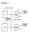
- FIG. 1 there is shown a block diagram of a single-chip microcomputer capable of embodying the ROM data protection system of the present invention.
- a CPU (central processing unit) 1 outputs a memory address through a memory address bus 2 to a ROM (read only memory) 4, and reads a instruction code through a system bus 3 from the ROM 4 so as to execute an given instruction such as a data transfer and an arithmetic and logic operation.
- An input port 5 is connected to the system bus 3, and also connected to external input terminals 7 This input port 5 is composed of an input buffer used when the CPU 1 reads through the system bus 3 the data inputted from the external input terminals 7.
- an output port 6 is connected to the system bus 3, and also connected to external output terminals 8. This output port 6 is composed of a data latch for temporarily holding data and an output buffer, which are used when the CPU 1 outputs data through the system bus 3 to the external output terminals 8.
- the ROM 4 is a mask ROM storing a user program.
- the ROM 4 receives through the memory address bus 2 the addresses sequentially outputted from the CPU 1 in accordance with progress of instruction execution in the CPU 1, and sequentially outputs instruction codes designated by the received addresses, to the system bus 3.
- the CPU 1 reads the instruction codes sequentially outputted on the system bus 3, and sequentially executes the received instructions.
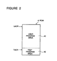
- the ROM 4 includes a user program area 40 starting from an address UADR and for storing a user program, and a test program area 42 starting from an address TADR and for storing a program which outputs all the codes stored in the ROM 4 through the output port 6 when the ROM 4 is to be tested.
- the test program area 42 are allocated with key data of N bytes which can be freely and individually determined or set when a user orders a ROM code, and a key number designation data "N" of one byte designating the number of bytes of the key data.
- the key data can be set to 255 bytes at maximum. Therefore, in the test program area, a user designated data area 44 of 256 bytes (including the key data area of 255 bytes and the key number designation data N of one byte) is reserved. Accordingly, the user orders ROM codes for not only the primary user program area 40 but also the user designated data area 44 included in the test program area 42.
- the key number designation data "N” is read out, and then, is set to a internal variable "n" (not shown) for the program processing (step 10). Thereafter, external input data is read out from the input port 5 (step 11), and the key data #1 is also read (step 12), so that the external input data and the key data #1 are compared (step 13). If coincidence is found, the internal variable "n” is decremented by "1” (step 14), and if the result of the decrement is not "0" (zero), the operation is branched or returned to the step 11 (step 15). Similarly, the operation from the step 11 to the step 14 is repeated for the key data #2 and the succeeding key data, until the decremented result of the internal variable "n" becomes "0".
- step 13 on the other hand, if the external input data is not consistent with the key data, a halt instruction is executed for stopping the operation of the CPU 1 (step 19). As a result, the execution of the succeeding test program is stopped.
- step 15 if the decremented internal variable "in” is "0" (zero), it is judged that all the key data collation has been properly and duly executed, and then, all the contents of the ROM 4 including the user program area are read out (step 16), and the read-out data is transferred or written to the output port 6 (step 17). If all the data of the ROM has been transferred, the processing based on the test program is completed (step 18).
- test signal 9 In an ordinary operation executed when the test signal 9 is at the logic value "0", it is not allowed to execute the instruction by inputting an instruction code from an external. Therefore, it is not possible to output the content of the ROM 4 to the external, other than to execute the user program. On the other hand, in the test mode in which the test signal 9 is at the logic value "1", the above mentioned test program is executed.
- a sequence of key or collation data individually previously designated by the user is inputted through the external input terminals 7 from a external device such as LSI tester, so that all the sequence of collation data inputted from the external device is compared with a sequence of key data #1 to #N internally stored, and if all data is consistent, all the data of the ROM 4 is outputted from the external output terminals 8 so that the ROM 4 is tested.
- a external device such as LSI tester
- FIG. 5 there is illustrated an operation timing of the test program.
- a system reset signal of an active-low type is cancelled under a condition in which the test signal 9 is set to "1"
- the test program is started.
- a timing for reading an external input data from the input port 5 in this program processing is designated by M1, M2, M3, ..., Mn, for the key data of N bytes, respectively.
- collation data #1, #2, #3, ..., #n are inputted through the external input terminals 7 from a LSI tester or others in the test of the ROM 4, it is necessary to input the collation data #1, #2, #3, ..., #n in time with the timings M1, M2, M3, .. ., Mn, respectively. Therefore, the switching or changing timing of the collation data is defined by an instruction execution timing of the test program in the CPU 1.
- the key data it is possible to set the key data of 255 bytes at maximum. However, it is possible to set the key data of an arbitrary byte number in accordance with a byte capacity of the ROM which is allowed to be used for the test program, and a desired level of protection.
- the second embodiment is characterized in that, in the test program for testing the content of the ROM 1 in the single-chip microcomputer of the first embodiment, a plurality of items of key data are sequentially compared or collated with a corresponding number of items of input data supplied through the input port 5 from an external, at a timing which can be arbitrarily set. Accordingly, the same microcomputer as that used in the first embodiment and therefore shown in Figure 1 is used in the second embodiment. Therefore, the detailed description of the microcomputer will be omitted.
- the test program area of the ROM 4 in the second embodiment is allocated with key data of three bytes which can be freely and individually determined or set when a user orders a ROM code, and a timer data "T" of one byte designating a timing of execution of the test program. Therefore, in the test program area, a user designated data area 46 of 4 bytes is reserved. Accordingly, the user orders ROM codes for not only the primary user program area 40 but also the user designated data area 46 included in the test program area 42.
- the timer data "T” is read out (step 20), and then, is set to an internal variable "t" (not shown) for the program processing. Thereafter, external input data is read out from the input port 5 (step 21), and the key data #1 is also read (step 22), so that the external input data and the key data #1 are compared (step 23). If coincidence is found in the step 23, whether or not all the key data of the three bytes have been compared is checked (step 24). In the step 24, it is detected that the comparison or collation of all the key data of the three bytes has not yet been completed, the internal variable "t" is decremented by "1" (step 25). This decrement is repeated until the result of the decrement becomes "0" (zero) (step 26).
- the operation is branched to the step 21. Similarly, the operation including the setting of the internal variable "t" and from the step 21 to the step 26 is repeated for the key data #2 and the succeeding key data #3.
- a halt instruction is executed for stopping the operation of the CPU 1 (step 30). As a result, the execution of the succeeding test program is stopped.
- step 24 if the comparison or collation of all the key data of the three bytes has been completed, it is deemed that all the key data collation has been properly and duly executed, and then, all the contents of the ROM 4 including the user program area is read out (step 27), and the read-out data is transferred or written to the output port 6 (step 28). If all the data of the ROM has been transferred, the processing based on the test program is completed (step 29).
- test signal 9 in an ordinary operation executed when the test signal 9 is at the logic value "0", it is not allowed to execute the instruction by inputting an instruction code from an external, and therefore, it is not possible to output the content of the ROM 4 to the external, other than to execute the user program.
- test mode in which the test signal 9 is at the logic value "1 ", the above mentioned test program is executed.
- the key or collation data of three bytes individually previously designated by the user is inputted through the external input terminals 7 from an external device such as LSI tester, so that all the collation data inputted from the external device is compared with all the key data stored in the ROM, and if coincidence of all data is found, all the data of the ROM 4 is outputted from the external output terminals 8 for the testing of the ROM 4.
- an external device such as LSI tester
- FIG. 8 there is illustrated a operation timing of the test program in the second embodiment.
- a system reset signal of an active-low type is cancelled under a condition in which the test signal 9 is set to "1"
- the test program is started.
- a timing for reading an external input data from the input port 5 in this program processing (step 21) is designated by M1, M2 and M3 for the key data of three bytes, respectively.
- Each interval between each pair of adjacent ones of the timings M1, M2 and M3 is designated by "I”. This interval "I” is defined by using the set value of the timer data "T" as a variable, and ensured by the counting processing in the steps 25 and 26.
- the switching or changing timing of the collation data is defined with the interval "I", the value of which is arbitrarily set by setting a value of the timer data "T".
- the key data of three bytes it is possible to set the key data of three bytes. However, it is possible to set the key data of an arbitrary byte number in accordance with a byte capacity of the ROM which is allowed to be used for the test program, and a desired level of protection.
- the ROM data protection system in accordance with the present invention is characterized in that when the ROM of the single-chip microcomputer is tested, it is necessary, before the testing, to previously supply a plurality of items (or bytes) of collation information while switching or changing at a predetermined timing or interval, and only when all the of items of collation information are completely consistent with a plurality of items (or bytes) of internal key information, the ROM data is allowed to be outputted to the external output terminals. Therefore, it is possible to obtain protection of a level which is remarkably higher than the prior art password system in which only a simple data comparison is executed.
- the present invention has a high degree of advantage in a practical use.
- the one-chip microcomputer in accordance with the present invention is inexpensive.
Abstract
Description
- The present invention relates to a microcomputer including therein a read only memory (ROM), and more specifically to a microcomputer having a function of protecting a content of a ROM.
- Recently, microcomputers are widely used in various fields including office automation instruments and domestic instruments. In the instruments or systems incorporating therein the microcomputer, it is possible to copy the system by analyzing or copying a program describing a control sequence of the system. On the other hand, in systems such as IC cards (chip card) and POS (point of sales) systems, which handle money information and individual information, there is possibility that the system is used by an unauthorized person by analyzing the program.
- The above mentioned problems concerning information security has recently become important more and more, and it has become indispensable to realize a system capable of completely protecting the right and interest of a proper proprietor.
- In order to solve the above mentioned problems, it is an ordinary practice to store a program in a ROM internally provided in the microcomputer, and to inhibit a reading of the content of the ROM to an external terminal. In this case, it is necessary to provide a test mode for testing an LSI and analyzing the LSI when a defective is found, and to allow the content of the ROM to be read out to the external terminal only in the test mode. Furthermore, it is necessary to internally provide a function of protecting the read-out data.
- A main system currently used for protecting the ROM data includes a password system in which an internal special data is compared with a cipher code inputted from the external terminal, and a data output is controlled on the basis of the result of the comparison, and an encryption system in which the ROM data is encryted.
- The password system is disclosed in for example Japanese Patent Application Laid-open No. 60-123948, in which a mask ROM is connected through an output buffer to an external terminal, and on the other hand, a control code memory is provided to be written with control codes ordered or determined at the same time as a content of the mask ROM is ordered. A code designation memory is connected to the external terminal so that the code designation memory stores a code inputted through the external terminal. A code comparator compares a content of the control code memory with a content of the code designation memory, and when the content of the control code memory is consistent with the content of the code designation memory, the code comparator outputs an active control signal to the output buffer, so that the output buffer is brought into an output allowance condition. If the content of the control code memory is not consistent with the content of the code designation memory, the code comparator renders the control signal inactive, so that the output buffer is put in an output inhibition condition.
- With the above mentioned arrangement, unless the same code as a predetermined code is given from an external before reading out the content of the ROM, it is impossible to read out the content of the ROM to the external terminal.
- In general, however, the password system is difficult to give a high degree of security. For example, in the above mentioned prior art protection system of the password type, since a simple code comparison is executed only one time, the level of protection is low. In this case, even if the code length or bit length is elongated, an increase of the protection level corresponding to an increase of hardware in the code designation memory and the code comparator cannot be obtained.
- As a means for solving the above mentioned problems, it is considered to use the encryption system. In this case, however, a hardware exclusively used for encryption and decryptment is required. In addition, it is possible to provide different encryption rules for all users who order the ROM code. Accordingly, it is not suitable to a generalized use.
- Accordingly, it is an object of the present invention to provide a ROM data protection system which has overcome the above mentioned defect of the conventional one.
- Another object of the present invention is to provide a microcomputer having a ROM data protection system which has overcome the above mentioned defect of the conventional one, and which gives a high degree of protection with a minimum amount of hardware.
- The above and other objects of the present invention are achieved in accordance with the present invention by a microcomputer including a program read only memory storing a program; a central processing means executing the program read out from the program read only memory for a data processing; an external data input means receiving data to be processed by the central processing means, from an external device; and an external data output means for outputting the data processed by the central processing means to an external device. The program read only memory also stores a test program for testing the program read only memory and a plurality of items of collation information. The central processing means has a test mode in which the central processing means executes the test program, and compares all the plurality of items of collation information with a corresponding number of items of data sequentially inputted through the external input means, by selecting one of the plurality of items of collation information and comparing the selected item of collation information with one item of data inputted through the external input means when the selected item of collation information is selected. Only when all the plurality of items of collation information are consistent with all the items of data sequentially inputted through the external input means, the central processing means allowing all contents stored in the program read only memory to be outputted through the external output means.
- The above and other objects, features and advantages of the present invention will be apparent from the following description of preferred embodiments of the invention with reference to the accompanying drawings.
-
- Figure 1 is a block diagram of a single-chip microcomputer capable of embodying the ROM data protection system of the present invention;
- Figure 2 illustrates an address map of the ROM incorporated in the microcomputer shown in Figure 1;
- Figure 3 illustrates a user designated area in a test program region of the ROM incorporated in the microcomputer shown in Figure 1 in a first embodiment of the present invention;
- Figure 4 is a flow chart of a test program in the first embodiment of the present invention;
- Figure 5 is a timing chart of the test program in the first embodiment of the present invention;
- Figure 6 illustrates a user designated area in a test program region of the ROM incorporated in the microcomputer shown in Figure 1 in a second embodiment of the present invention;
- Figure 7 is a flow chart of a test program in the second embodiment of the present invention; and
- Figure 8 is a timing chart of the test program in the second embodiment of the present invention.
- Referring to Figure 1, there is shown a block diagram of a single-chip microcomputer capable of embodying the ROM data protection system of the present invention.
- A CPU (central processing unit) 1 outputs a memory address through a
memory address bus 2 to a ROM (read only memory) 4, and reads a instruction code through asystem bus 3 from theROM 4 so as to execute an given instruction such as a data transfer and an arithmetic and logic operation. Aninput port 5 is connected to thesystem bus 3, and also connected toexternal input terminals 7 Thisinput port 5 is composed of an input buffer used when theCPU 1 reads through thesystem bus 3 the data inputted from theexternal input terminals 7. On the other hand, anoutput port 6 is connected to thesystem bus 3, and also connected toexternal output terminals 8. Thisoutput port 6 is composed of a data latch for temporarily holding data and an output buffer, which are used when theCPU 1 outputs data through thesystem bus 3 to theexternal output terminals 8. - The
ROM 4 is a mask ROM storing a user program. TheROM 4 receives through thememory address bus 2 the addresses sequentially outputted from theCPU 1 in accordance with progress of instruction execution in theCPU 1, and sequentially outputs instruction codes designated by the received addresses, to thesystem bus 3. TheCPU 1 reads the instruction codes sequentially outputted on thesystem bus 3, and sequentially executes the received instructions. - Referring to Figure 2, a memory map of the
ROM 4 is illustrated. TheROM 4 includes auser program area 40 starting from an address UADR and for storing a user program, and atest program area 42 starting from an address TADR and for storing a program which outputs all the codes stored in theROM 4 through theoutput port 6 when theROM 4 is to be tested. - Here, after the CPU resets the system, if the CPU releases the reset condition when the
CPU 1 shown in Figure 1 is in receipt of atest signal 9 of a logical value "0", the CPU initializes a start address to "UADR" for execution of instructions. On the other hand, after the CPU resets the system, if the CPU releases the reset condition when theCPU 1 shown in Figure 1 is in receipt of thetest signal 9 of a logical value "1", the CPU initializes initializes the start address to "TADR" for execution of instructions. - As shown in Figure 3, the
test program area 42 are allocated with key data of N bytes which can be freely and individually determined or set when a user orders a ROM code, and a key number designation data "N" of one byte designating the number of bytes of the key data. The key data can be set to 255 bytes at maximum. Therefore, in the test program area, a user designateddata area 44 of 256 bytes (including the key data area of 255 bytes and the key number designation data N of one byte) is reserved. Accordingly, the user orders ROM codes for not only the primaryuser program area 40 but also the user designateddata area 44 included in thetest program area 42. - Now, a processing of the above mentioned test program will be described with the flow chart of Figure 4.
- First, the key number designation data "N" is read out, and then, is set to a internal variable "n" (not shown) for the program processing (step 10). Thereafter, external input data is read out from the input port 5 (step 11), and the
key data # 1 is also read (step 12), so that the external input data and thekey data # 1 are compared (step 13). If coincidence is found, the internal variable "n" is decremented by "1" (step 14), and if the result of the decrement is not "0" (zero), the operation is branched or returned to the step 11 (step 15). Similarly, the operation from the step 11 to thestep 14 is repeated for thekey data # 2 and the succeeding key data, until the decremented result of the internal variable "n" becomes "0". - In the
step 13, on the other hand, if the external input data is not consistent with the key data, a halt instruction is executed for stopping the operation of the CPU 1 (step 19). As a result, the execution of the succeeding test program is stopped. - In the
step 15, if the decremented internal variable "in" is "0" (zero), it is judged that all the key data collation has been properly and duly executed, and then, all the contents of theROM 4 including the user program area are read out (step 16), and the read-out data is transferred or written to the output port 6 (step 17). If all the data of the ROM has been transferred, the processing based on the test program is completed (step 18). - In an ordinary operation executed when the
test signal 9 is at the logic value "0", it is not allowed to execute the instruction by inputting an instruction code from an external. Therefore, it is not possible to output the content of theROM 4 to the external, other than to execute the user program. On the other hand, in the test mode in which thetest signal 9 is at the logic value "1", the above mentioned test program is executed. A sequence of key or collation data individually previously designated by the user is inputted through theexternal input terminals 7 from a external device such as LSI tester, so that all the sequence of collation data inputted from the external device is compared with a sequence ofkey data # 1 to #N internally stored, and if all data is consistent, all the data of theROM 4 is outputted from theexternal output terminals 8 so that theROM 4 is tested. - Referring to Figure 5, there is illustrated an operation timing of the test program. In the timing chart shown in Figure 5, if a system reset signal of an active-low type is cancelled under a condition in which the
test signal 9 is set to "1", the test program is started. A timing for reading an external input data from theinput port 5 in this program processing (step 11) is designated by M1, M2, M3, ..., Mn, for the key data of N bytes, respectively. - Therefore, when
collation data # 1, #2, #3, ..., #n are inputted through theexternal input terminals 7 from a LSI tester or others in the test of theROM 4, it is necessary to input thecollation data # 1, #2, #3, ..., #n in time with the timings M1, M2, M3, .. ., Mn, respectively. Therefore, the switching or changing timing of the collation data is defined by an instruction execution timing of the test program in theCPU 1. - In the first embodiment, it is possible to set the key data of 255 bytes at maximum. However, it is possible to set the key data of an arbitrary byte number in accordance with a byte capacity of the ROM which is allowed to be used for the test program, and a desired level of protection.
- Now, a second embodiment of the present invention will be described. The second embodiment is characterized in that, in the test program for testing the content of the
ROM 1 in the single-chip microcomputer of the first embodiment, a plurality of items of key data are sequentially compared or collated with a corresponding number of items of input data supplied through theinput port 5 from an external, at a timing which can be arbitrarily set. Accordingly, the same microcomputer as that used in the first embodiment and therefore shown in Figure 1 is used in the second embodiment. Therefore, the detailed description of the microcomputer will be omitted. - As shown in Figure 6, the test program area of the
ROM 4 in the second embodiment is allocated with key data of three bytes which can be freely and individually determined or set when a user orders a ROM code, and a timer data "T" of one byte designating a timing of execution of the test program. Therefore, in the test program area, a user designateddata area 46 of 4 bytes is reserved. Accordingly, the user orders ROM codes for not only the primaryuser program area 40 but also the user designateddata area 46 included in thetest program area 42. - Now, a processing of the test program in the second embodiment will be described with the flow chart of Figure 7.
- First, the timer data "T" is read out (step 20), and then, is set to an internal variable "t" (not shown) for the program processing. Thereafter, external input data is read out from the input port 5 (step 21), and the
key data # 1 is also read (step 22), so that the external input data and thekey data # 1 are compared (step 23). If coincidence is found in the step 23, whether or not all the key data of the three bytes have been compared is checked (step 24). In thestep 24, it is detected that the comparison or collation of all the key data of the three bytes has not yet been completed, the internal variable "t" is decremented by "1" (step 25). This decrement is repeated until the result of the decrement becomes "0" (zero) (step 26). If the result of the decrement is "0" (zero), the operation is branched to the step 21. Similarly, the operation including the setting of the internal variable "t" and from the step 21 to thestep 26 is repeated for thekey data # 2 and the succeedingkey data # 3. - Here, if the external input data is not consistent with the key data in the step 23, a halt instruction is executed for stopping the operation of the CPU 1 (step 30). As a result, the execution of the succeeding test program is stopped.
- In the
step 24, if the comparison or collation of all the key data of the three bytes has been completed, it is deemed that all the key data collation has been properly and duly executed, and then, all the contents of theROM 4 including the user program area is read out (step 27), and the read-out data is transferred or written to the output port 6 (step 28). If all the data of the ROM has been transferred, the processing based on the test program is completed (step 29). - Similarly to the single-chip microcomputer of the first embodiment, in an ordinary operation executed when the
test signal 9 is at the logic value "0", it is not allowed to execute the instruction by inputting an instruction code from an external, and therefore, it is not possible to output the content of theROM 4 to the external, other than to execute the user program. On the other hand, in the test mode in which thetest signal 9 is at the logic value "1 ", the above mentioned test program is executed. The key or collation data of three bytes individually previously designated by the user is inputted through theexternal input terminals 7 from an external device such as LSI tester, so that all the collation data inputted from the external device is compared with all the key data stored in the ROM, and if coincidence of all data is found, all the data of theROM 4 is outputted from theexternal output terminals 8 for the testing of theROM 4. - Referring to Figure 8, there is illustrated a operation timing of the test program in the second embodiment. In the timing chart shown in Figure 8, if a system reset signal of an active-low type is cancelled under a condition in which the
test signal 9 is set to "1", the test program is started. A timing for reading an external input data from theinput port 5 in this program processing (step 21) is designated by M1, M2 and M3 for the key data of three bytes, respectively. Each interval between each pair of adjacent ones of the timings M1, M2 and M3 is designated by "I". This interval "I" is defined by using the set value of the timer data "T" as a variable, and ensured by the counting processing in thesteps - Therefore, when collation data is inputted through the
external input terminals 7 from an LSI tester or others in the test of theROM 4, it is necessary to input the collation data in time with the timings M1, M2 and M3, respectively. Therefore, the switching or changing timing of the collation data is defined with the interval "I", the value of which is arbitrarily set by setting a value of the timer data "T". - In the second embodiment, it is possible to set the key data of three bytes. However, it is possible to set the key data of an arbitrary byte number in accordance with a byte capacity of the ROM which is allowed to be used for the test program, and a desired level of protection.
- As seen from the above description of the embodiments, the ROM data protection system in accordance with the present invention is characterized in that when the ROM of the single-chip microcomputer is tested, it is necessary, before the testing, to previously supply a plurality of items (or bytes) of collation information while switching or changing at a predetermined timing or interval, and only when all the of items of collation information are completely consistent with a plurality of items (or bytes) of internal key information, the ROM data is allowed to be outputted to the external output terminals. Therefore, it is possible to obtain protection of a level which is remarkably higher than the prior art password system in which only a simple data comparison is executed.
- In addition, when a user orders ROM codes, it is possible to individually freely determine or set the collation information and the processing variables used in the collation or comparison, and also, it is easily modify and change the collation information and the processing variables. Therefore, the present invention has a high degree of advantage in a practical use.
- Furthermore, since the collation is realized by utilizing existing hardware resources including the CPU and the input/output ports which are internally provided in the microcomputer, without using a special additional hardware, the one-chip microcomputer in accordance with the present invention is inexpensive.
- The invention has thus been shown and described with reference to the specific embodiments. However, it should be noted that the present invention is in no way limited to the details of the illustrated structures but changes and modifications may be made within the scope of the appended claims.
Claims (7)
Applications Claiming Priority (2)
| Application Number | Priority Date | Filing Date | Title |
|---|---|---|---|
| JP2199551A JPH0484348A (en) | 1990-07-27 | 1990-07-27 | Rom data protecting system |
| JP199551/90 | 1990-07-27 |
Publications (3)
| Publication Number | Publication Date |
|---|---|
| EP0468535A2 true EP0468535A2 (en) | 1992-01-29 |
| EP0468535A3 EP0468535A3 (en) | 1992-07-01 |
| EP0468535B1 EP0468535B1 (en) | 1999-01-13 |
Family
ID=16409711
Family Applications (1)
| Application Number | Title | Priority Date | Filing Date |
|---|---|---|---|
| EP91112738A Expired - Lifetime EP0468535B1 (en) | 1990-07-27 | 1991-07-29 | Microcomputer having ROM data protection function |
Country Status (4)
| Country | Link |
|---|---|
| US (1) | US5671394A (en) |
| EP (1) | EP0468535B1 (en) |
| JP (1) | JPH0484348A (en) |
| DE (1) | DE69130750T2 (en) |
Cited By (3)
| Publication number | Priority date | Publication date | Assignee | Title |
|---|---|---|---|---|
| US5615263A (en) * | 1995-01-06 | 1997-03-25 | Vlsi Technology, Inc. | Dual purpose security architecture with protected internal operating system |
| GB2311152A (en) * | 1996-03-11 | 1997-09-17 | Vlsi Technology Inc | Dual mode security architecture with protected internal operating system |
| US6754830B1 (en) | 1999-02-26 | 2004-06-22 | Nokia Multimedia Terminals Oy | Method and coupling arrangement for preventing unauthorized access to a microprocessor |
Families Citing this family (11)
| Publication number | Priority date | Publication date | Assignee | Title |
|---|---|---|---|---|
| DE4341082A1 (en) * | 1993-12-02 | 1995-06-08 | Teves Gmbh Alfred | Circuit arrangement for safety-critical control systems |
| US6493825B1 (en) * | 1998-06-29 | 2002-12-10 | Emc Corporation | Authentication of a host processor requesting service in a data processing network |
| JP3606788B2 (en) * | 2000-05-31 | 2005-01-05 | 松下電器産業株式会社 | Semiconductor integrated circuit and inspection method for semiconductor integrated circuit |
| EP1295200A2 (en) * | 2000-06-12 | 2003-03-26 | Koninklijke Philips Electronics N.V. | Data processing method and device for protected execution of instructions |
| JP4489915B2 (en) * | 2000-07-31 | 2010-06-23 | 大日本印刷株式会社 | Portable information processing device with password verification function |
| CN1162783C (en) * | 2001-11-09 | 2004-08-18 | 汪文虎 | Information security method |
| US7266848B2 (en) * | 2002-03-18 | 2007-09-04 | Freescale Semiconductor, Inc. | Integrated circuit security and method therefor |
| JP4182740B2 (en) * | 2002-12-06 | 2008-11-19 | 沖電気工業株式会社 | Microcomputer |
| JP2007094632A (en) * | 2005-09-28 | 2007-04-12 | Fujitsu Ltd | Security protecting device |
| KR100791838B1 (en) * | 2006-10-18 | 2008-01-07 | 삼성전자주식회사 | Smart card and method for testing of smart card |
| US9619647B2 (en) * | 2015-05-07 | 2017-04-11 | Nxp Usa, Inc. | Integrated circuit access |
Citations (2)
| Publication number | Priority date | Publication date | Assignee | Title |
|---|---|---|---|---|
| JPS60123948A (en) * | 1983-12-08 | 1985-07-02 | Nec Corp | System for controlling readout of rom |
| USH714H (en) * | 1987-10-26 | 1989-11-07 | The United States Of America As Represented By The Secretary Of The Navy | Serial data word processing arrangement |
Family Cites Families (9)
| Publication number | Priority date | Publication date | Assignee | Title |
|---|---|---|---|---|
| US4228424A (en) * | 1978-10-16 | 1980-10-14 | Baker Protective Services, Incorporated | Central station alarm |
| US4450560A (en) * | 1981-10-09 | 1984-05-22 | Teradyne, Inc. | Tester for LSI devices and memory devices |
| JPS59191650A (en) * | 1983-04-15 | 1984-10-30 | Hitachi Ltd | Preventing system for wrong use of system |
| US4812994A (en) * | 1985-08-06 | 1989-03-14 | Pitney Bowes Inc. | Postage meter locking system |
| JPH081606B2 (en) * | 1986-04-23 | 1996-01-10 | 日本電気株式会社 | Single chip microcomputer |
| JPS62272325A (en) * | 1986-05-21 | 1987-11-26 | Hitachi Ltd | Data processor |
| US4937855A (en) * | 1988-02-09 | 1990-06-26 | Viscount Industries Limited | Building security system |
| US5014191A (en) * | 1988-05-02 | 1991-05-07 | Padgaonkar Ajay J | Security for digital signal processor program memory |
| JPH021019A (en) * | 1988-12-02 | 1990-01-05 | Hitachi Ltd | One-chip microcomputer |
-
1990
- 1990-07-27 JP JP2199551A patent/JPH0484348A/en active Pending
-
1991
- 1991-07-29 DE DE69130750T patent/DE69130750T2/en not_active Expired - Fee Related
- 1991-07-29 EP EP91112738A patent/EP0468535B1/en not_active Expired - Lifetime
-
1994
- 1994-09-27 US US08/313,534 patent/US5671394A/en not_active Expired - Fee Related
Patent Citations (2)
| Publication number | Priority date | Publication date | Assignee | Title |
|---|---|---|---|---|
| JPS60123948A (en) * | 1983-12-08 | 1985-07-02 | Nec Corp | System for controlling readout of rom |
| USH714H (en) * | 1987-10-26 | 1989-11-07 | The United States Of America As Represented By The Secretary Of The Navy | Serial data word processing arrangement |
Non-Patent Citations (2)
| Title |
|---|
| ELECTRONIC DESIGN. vol. 32, no. 5, March 1983, HASBROUCK HEIGHTS, NEW JERSEY pages 129 - 134; 'MICROCOMPUTER'S MEMORIES SOLVE TESTING AND FIRMWARE PROBLEMS' * |
| PATENT ABSTRACTS OF JAPAN vol. 9, no. 281 (P-403)(2004) 8 November 1985 & JP-A-60 123 948 ( NIPPON DENKI KK ) 2 July 1985 * |
Cited By (3)
| Publication number | Priority date | Publication date | Assignee | Title |
|---|---|---|---|---|
| US5615263A (en) * | 1995-01-06 | 1997-03-25 | Vlsi Technology, Inc. | Dual purpose security architecture with protected internal operating system |
| GB2311152A (en) * | 1996-03-11 | 1997-09-17 | Vlsi Technology Inc | Dual mode security architecture with protected internal operating system |
| US6754830B1 (en) | 1999-02-26 | 2004-06-22 | Nokia Multimedia Terminals Oy | Method and coupling arrangement for preventing unauthorized access to a microprocessor |
Also Published As
| Publication number | Publication date |
|---|---|
| EP0468535B1 (en) | 1999-01-13 |
| US5671394A (en) | 1997-09-23 |
| JPH0484348A (en) | 1992-03-17 |
| DE69130750D1 (en) | 1999-02-25 |
| DE69130750T2 (en) | 1999-09-02 |
| EP0468535A3 (en) | 1992-07-01 |
Similar Documents
| Publication | Publication Date | Title |
|---|---|---|
| EP0468535B1 (en) | Microcomputer having ROM data protection function | |
| US5206938A (en) | Ic card with memory area protection based on address line restriction | |
| US4777355A (en) | IC card and system for checking the functionality thereof | |
| JP3459649B2 (en) | Data exchange system including portable data processing unit | |
| US4908038A (en) | High-security integrated-circuit card | |
| US5237616A (en) | Secure computer system having privileged and unprivileged memories | |
| US5224160A (en) | Process for securing and for checking the integrity of the secured programs | |
| US7720939B1 (en) | Method for transforming and verifying downloaded program fragments with data type restrictions and corresponding system | |
| US4905142A (en) | Semiconductor integrated circuit device with built-in arrangement for memory testing | |
| US7434264B2 (en) | Data processing system with peripheral access protection and method therefor | |
| US5249294A (en) | Determination of time of execution of predetermined data processing routing in relation to occurrence of prior externally observable event | |
| US5404539A (en) | Data driven information processor with ring comparing comparator | |
| JPS6270993A (en) | Portable data carrier for storing and processing data | |
| EP0694828A2 (en) | Data processor with secure communication | |
| US6536034B1 (en) | Method for modifying code sequences and related device | |
| CA2037857C (en) | Prevention of determination of time of execution of predetermined data processing routine in relation to occurrence of prior observable external event | |
| US5159183A (en) | Ic card | |
| US7447916B2 (en) | Blocking of the operation of an integrated circuit | |
| EP0518479B1 (en) | Processing system and method including memory selection | |
| JPH04215194A (en) | Ic card | |
| US5781796A (en) | System for automatic configuration of I/O base address without configuration program using readout data on common bus by responding device | |
| US5729004A (en) | Data communication device and method of a smart card | |
| US6742073B1 (en) | Bus controller technique to control N buses | |
| JPH04205082A (en) | Portable electronic apparatus | |
| GB2129586A (en) | Improvements in or relating to memory systems |
Legal Events
| Date | Code | Title | Description |
|---|---|---|---|
| PUAI | Public reference made under article 153(3) epc to a published international application that has entered the european phase |
Free format text: ORIGINAL CODE: 0009012 |
|
| 17P | Request for examination filed |
Effective date: 19910827 |
|
| AK | Designated contracting states |
Kind code of ref document: A2 Designated state(s): DE FR GB |
|
| PUAL | Search report despatched |
Free format text: ORIGINAL CODE: 0009013 |
|
| AK | Designated contracting states |
Kind code of ref document: A3 Designated state(s): DE FR GB |
|
| 17Q | First examination report despatched |
Effective date: 19970624 |
|
| GRAG | Despatch of communication of intention to grant |
Free format text: ORIGINAL CODE: EPIDOS AGRA |
|
| GRAG | Despatch of communication of intention to grant |
Free format text: ORIGINAL CODE: EPIDOS AGRA |
|
| GRAH | Despatch of communication of intention to grant a patent |
Free format text: ORIGINAL CODE: EPIDOS IGRA |
|
| GRAH | Despatch of communication of intention to grant a patent |
Free format text: ORIGINAL CODE: EPIDOS IGRA |
|
| GRAA | (expected) grant |
Free format text: ORIGINAL CODE: 0009210 |
|
| AK | Designated contracting states |
Kind code of ref document: B1 Designated state(s): DE FR GB |
|
| REF | Corresponds to: |
Ref document number: 69130750 Country of ref document: DE Date of ref document: 19990225 |
|
| ET | Fr: translation filed | ||
| PLBE | No opposition filed within time limit |
Free format text: ORIGINAL CODE: 0009261 |
|
| STAA | Information on the status of an ep patent application or granted ep patent |
Free format text: STATUS: NO OPPOSITION FILED WITHIN TIME LIMIT |
|
| 26N | No opposition filed | ||
| REG | Reference to a national code |
Ref country code: GB Ref legal event code: IF02 |
|
| PGFP | Annual fee paid to national office [announced via postgrant information from national office to epo] |
Ref country code: FR Payment date: 20020709 Year of fee payment: 12 |
|
| PGFP | Annual fee paid to national office [announced via postgrant information from national office to epo] |
Ref country code: GB Payment date: 20020724 Year of fee payment: 12 |
|
| PGFP | Annual fee paid to national office [announced via postgrant information from national office to epo] |
Ref country code: DE Payment date: 20020807 Year of fee payment: 12 |
|
| PG25 | Lapsed in a contracting state [announced via postgrant information from national office to epo] |
Ref country code: GB Free format text: LAPSE BECAUSE OF NON-PAYMENT OF DUE FEES Effective date: 20030729 |
|
| PG25 | Lapsed in a contracting state [announced via postgrant information from national office to epo] |
Ref country code: DE Free format text: LAPSE BECAUSE OF NON-PAYMENT OF DUE FEES Effective date: 20040203 |
|
| GBPC | Gb: european patent ceased through non-payment of renewal fee |
Effective date: 20030729 |
|
| PG25 | Lapsed in a contracting state [announced via postgrant information from national office to epo] |
Ref country code: FR Free format text: LAPSE BECAUSE OF NON-PAYMENT OF DUE FEES Effective date: 20040331 |
|
| REG | Reference to a national code |
Ref country code: FR Ref legal event code: ST |