EP0354793B1 - IC card and method for rewriting its program - Google Patents
IC card and method for rewriting its program Download PDFInfo
- Publication number
- EP0354793B1 EP0354793B1 EP19890308141 EP89308141A EP0354793B1 EP 0354793 B1 EP0354793 B1 EP 0354793B1 EP 19890308141 EP19890308141 EP 19890308141 EP 89308141 A EP89308141 A EP 89308141A EP 0354793 B1 EP0354793 B1 EP 0354793B1
- Authority
- EP
- European Patent Office
- Prior art keywords
- program
- sub
- area
- card
- management information
- Prior art date
- Legal status (The legal status is an assumption and is not a legal conclusion. Google has not performed a legal analysis and makes no representation as to the accuracy of the status listed.)
- Revoked
Links
Images

Classifications
-
- G—PHYSICS
- G07—CHECKING-DEVICES
- G07F—COIN-FREED OR LIKE APPARATUS
- G07F7/00—Mechanisms actuated by objects other than coins to free or to actuate vending, hiring, coin or paper currency dispensing or refunding apparatus
- G07F7/08—Mechanisms actuated by objects other than coins to free or to actuate vending, hiring, coin or paper currency dispensing or refunding apparatus by coded identity card or credit card or other personal identification means
- G07F7/10—Mechanisms actuated by objects other than coins to free or to actuate vending, hiring, coin or paper currency dispensing or refunding apparatus by coded identity card or credit card or other personal identification means together with a coded signal, e.g. in the form of personal identification information, like personal identification number [PIN] or biometric data
- G07F7/1008—Active credit-cards provided with means to personalise their use, e.g. with PIN-introduction/comparison system
-
- G—PHYSICS
- G06—COMPUTING; CALCULATING OR COUNTING
- G06Q—INFORMATION AND COMMUNICATION TECHNOLOGY [ICT] SPECIALLY ADAPTED FOR ADMINISTRATIVE, COMMERCIAL, FINANCIAL, MANAGERIAL OR SUPERVISORY PURPOSES; SYSTEMS OR METHODS SPECIALLY ADAPTED FOR ADMINISTRATIVE, COMMERCIAL, FINANCIAL, MANAGERIAL OR SUPERVISORY PURPOSES, NOT OTHERWISE PROVIDED FOR
- G06Q20/00—Payment architectures, schemes or protocols
- G06Q20/30—Payment architectures, schemes or protocols characterised by the use of specific devices or networks
- G06Q20/34—Payment architectures, schemes or protocols characterised by the use of specific devices or networks using cards, e.g. integrated circuit [IC] cards or magnetic cards
- G06Q20/341—Active cards, i.e. cards including their own processing means, e.g. including an IC or chip
-
- G—PHYSICS
- G06—COMPUTING; CALCULATING OR COUNTING
- G06Q—INFORMATION AND COMMUNICATION TECHNOLOGY [ICT] SPECIALLY ADAPTED FOR ADMINISTRATIVE, COMMERCIAL, FINANCIAL, MANAGERIAL OR SUPERVISORY PURPOSES; SYSTEMS OR METHODS SPECIALLY ADAPTED FOR ADMINISTRATIVE, COMMERCIAL, FINANCIAL, MANAGERIAL OR SUPERVISORY PURPOSES, NOT OTHERWISE PROVIDED FOR
- G06Q20/00—Payment architectures, schemes or protocols
- G06Q20/30—Payment architectures, schemes or protocols characterised by the use of specific devices or networks
- G06Q20/34—Payment architectures, schemes or protocols characterised by the use of specific devices or networks using cards, e.g. integrated circuit [IC] cards or magnetic cards
- G06Q20/355—Personalisation of cards for use
- G06Q20/3552—Downloading or loading of personalisation data
-
- G—PHYSICS
- G06—COMPUTING; CALCULATING OR COUNTING
- G06Q—INFORMATION AND COMMUNICATION TECHNOLOGY [ICT] SPECIALLY ADAPTED FOR ADMINISTRATIVE, COMMERCIAL, FINANCIAL, MANAGERIAL OR SUPERVISORY PURPOSES; SYSTEMS OR METHODS SPECIALLY ADAPTED FOR ADMINISTRATIVE, COMMERCIAL, FINANCIAL, MANAGERIAL OR SUPERVISORY PURPOSES, NOT OTHERWISE PROVIDED FOR
- G06Q20/00—Payment architectures, schemes or protocols
- G06Q20/30—Payment architectures, schemes or protocols characterised by the use of specific devices or networks
- G06Q20/34—Payment architectures, schemes or protocols characterised by the use of specific devices or networks using cards, e.g. integrated circuit [IC] cards or magnetic cards
- G06Q20/355—Personalisation of cards for use
- G06Q20/3555—Personalisation of two or more cards
-
- G—PHYSICS
- G06—COMPUTING; CALCULATING OR COUNTING
- G06Q—INFORMATION AND COMMUNICATION TECHNOLOGY [ICT] SPECIALLY ADAPTED FOR ADMINISTRATIVE, COMMERCIAL, FINANCIAL, MANAGERIAL OR SUPERVISORY PURPOSES; SYSTEMS OR METHODS SPECIALLY ADAPTED FOR ADMINISTRATIVE, COMMERCIAL, FINANCIAL, MANAGERIAL OR SUPERVISORY PURPOSES, NOT OTHERWISE PROVIDED FOR
- G06Q20/00—Payment architectures, schemes or protocols
- G06Q20/30—Payment architectures, schemes or protocols characterised by the use of specific devices or networks
- G06Q20/34—Payment architectures, schemes or protocols characterised by the use of specific devices or networks using cards, e.g. integrated circuit [IC] cards or magnetic cards
- G06Q20/357—Cards having a plurality of specified features
- G06Q20/3576—Multiple memory zones on card
- G06Q20/35765—Access rights to memory zones
Definitions
- the present invention relates to an IC card and a method for rewriting its program, and more particularly to a down-loadable IC card which is capable of rewriting its program quickly and a method for rewriting its processing program.
- the IC cards issued in accordance with several kinds of transactions contain their individual data contents to be processed by different processing procedures. Therefore, the processing programs for the IC cards are peculiar to the terminals or host computers (hereinafter represented by terminals) in which they are employed.
- These IC cards include a rewritable non-volatile memory at their information memory part in which a processing program is stored; and thus if the operation of an IC card is desired to be changed, its program can be rewritten.
- the program may include an application program and some parameters necessary for execution thereof.
- the parameters are constants, identification codes of the card and a user.
- the transfer error detection system becomes also complicated.
- JP-A-62-231,393 discloses an IC card containing a memory for storing data which is indexed, and is not concerned with the execution of program.
- FR-2,600,446 also discloses an IC card for storing indexed data.
- An aim of the present invention is to provide an IC card and a method for rewriting its program in which the rewrite can be done in a very short time only by transferring to the IC card a divided program including a part to be rewritten.
- Another aim of the present invention is to provide an IC card and a method for rewriting its program in which after a program is recorded in a plurality of divided programs in a memory area, if the size of the divided programs which are objects to be newly rewritten is made larger than that before the rewriting, they can be rewritten in accordance with their corresponding memory areas.
- a method for storing, rewriting and executing a program in an IC card having an input/output port for inputting a program to be down-loaded and outputting its processing result, a main storage area for storing data and programs, and a processor for sending the program input from the input/output port to said main storage area of the IC card, and a terminal for communicating commands to said IC card through said processor, the steps of the method comprising:
- the circuits arranged in the IC card include rewritable non-volatile memory means for storing the processing program to be executed by an ALU and management information for managing the areas where the processing program is stored in sub-areas of divisional programs; and means for writing, referring to the management information in accordance with the information specifying one or plural of the sub-areas input to the ALU, input programs in the sub-area(s).
- a region for storing attribute information including the leading address and area length of each of the sub-areas where the program parts are stored, as management information indicative of the reality of the areas. It is possible to set attribute information optionally.
- the processing program with any size composed of the program parts can be stored. Moreover, the above sub-areas can be optionally selected afterwards.
- rewriting the processing program it is not rewritten by transferring a whole program to an IC card but is partially rewritten only as to the sub-area storing the contents to be changed in the rewritable non-volatile memory, referring to the management information including the top address and area length of that sub-area previously stored in the IC card (the management information may be rewritten before writing the program parts if necessary).
- an IC card 1 is composed of an I/O part 2, an ALU or microprocessor unit (MPU) 3 and an information memory part 5 which may be rewritable non-volatile memory such as EEPROM.
- the I/O part 2 includes electrical contacts (not shown) on the surface of the IC card for inputting/outputting programs and for power supply. In place of the electrical contacts, electromagnetic induction may be adopted for downloading the program in the IC card.
- the information memory part 5 is composed of an application program memory section 7, an attribute information section 6 for storing management information for the areas of the program parts into which the application program to be stored in the application program memory 7 is divided, and data memory section 8 for storing several kinds of data.
- MPU 3 includes a system program memory 4 (e.g. mask ROM) in which a system program 4a for performing the hardware control of the IC card 1 is stored. By executing the system program 4a, MPU 3 performs the write/read of the program for the application program memory section 7 and the control of communication with terminal devices (e.g. IC card reader/writer incorporated therein). Moreover, MPU 3, by executing the system program 4a, performs the write of the attribute information transferred from an external device (the above terminal device) in the attribute information memory section 6 in accordance with an instruction transferred from the external device.
- a system program memory 4 e.g. mask ROM
- the application program memory section 7 is managed in the manner of dividing it into a plurality of memory areas, corresponding to a plurality of program parts of the application program to be stored therein, in accordance with the attribute information stored in the attribute information memory section 6.
- the application program is to be down-loaded, it is executed for each of dividable program parts. Now it is assumed that the processing program is equally divided into program parts each with e.g. 32 bytes. However, the unit of division is not limited to 32 bytes but may be optionally selected.
- the attribute information (Fig. 2a) about each of the areas storing each program part (32 bytes) received at the I/O part 2 is written in the attribute information memory section 6.
- the write of the attribute information is executed by activating the system program stored in the system program memory 4.
- the write of the application program is performed in accordance with the sequence as shown in Fig. 5.
- a write instruction specifying the program part area to be subjected to the write using discrimination information provided in accordance with the divided program parts, i.e. the area numbers, is transferred to the IC card 1 from the terminal device (not shown).
- MPU 3 of the IC card 1 aquires, in accordance with the above discrimination information, the top address, size, etc. of the pertinent program part memory area in the application program memory section 7 from the attribute information stored in the attribute information memory section 6 and prepares the write thereof.
- MPU 3 of the IC card 1 informs the terminal device of this fact through a data/control line 12 in accordance with the system program 4a.
- data to be written (one of the divided program parts constituting a part of the processing program, i.e. 32 bytes) is transferred from terminal device.
- MPU 3 executes the write of the transferred program part (write data), in accordance with the system program 4a, in the program part memory area (32 bytes) specified by the top or leading address and the size in the application program memory section 7 of the information memory part 5 of the IC card 1.
- the memory area is fixed to 32 bytes, the above acquisition of the size of the memory area may be omitted.
- discrimination information about the subsequent program part (32 bytes) is transferred from the terminal device in the same way.
- the program part (32 bytes) corresponding to the discrimination information is transferred from the terminal device.
- this program part is stored in the program part memory area specified in accordance with the attribute information decided by the precedently transferred discrimination information, In this way, the program parts of one processing program are sequentially stored by 32 bytes. As a result, the entire processing program will be stored as a collection of the program data parts in the application program memory section 7.
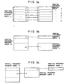
- Fig. 2a shows the relation between the entire processing program thus stored (a in Fig. 3a) and its program parts (b to g in Fig. 3a), and Fig. 2b shows the relation between the memory areas for storing the program parts (Fig. 2b) and their attribute information (Fig. 2a).
- the application program memory section 7 is divided into n (n: integer of 2 or more) program memory areas 7a to 7n.
- n integer of 2 or more
- the program part memory areas 7i to 7n are vacant areas reserved for rewrite.
- the order of writing the program parts may be optional since the write is performed in accordance with the numbers of the sub-areas, i.e. items of discrimination information.
- the attribute information is stored in a table form in the attribute information memory section 6.
- Program area numbers are stored at the heads of the respective rows as information for discriminating the program areas for storing the program parts and further spaces for storing the base address and size for each row are provided.
- the program area numbers, a, b, c, ... n in Fig. 2a correspond to the program part memory areas 7a, 7b, 7c, ... 7n with the same subscripts in Fig. 2b.
- aaaa, AA; bbbb, BB; cccc, CC; ... nnnn, NN in the respective spaces corresponding to the program area numbers a, b, c, ... n represent the base address and size thereof, respectively.
- the reason why both base address and size are provided is that although this is not required in the case the application program is managed in the equally divided program parts of 32 bytes, it is intended to manage the program in the program parts of any integer times of 32 bytes.
- the application program in the case where it is managed in the program divided parts is executed in the sequence of the above program area numbers, namely in the sequence of a, b, c, ... n this embodiment. Therefore, initially, as shown in Fig. 2b, the sequence of the program area numbers a, b, c, ... n accord with the sequence of arranging the program parts. And even if the sequence is changed by rewriting any program part, any problem does not occur since the previous program area numbers are retained.
- the processing program is not to be executed in the sequence of the numbers of program areas
- information for specifying the sequence of connecting the program parts in the respective memory areas is previously stored in the information memory section 5, or the program area number to be subsequently executed is previously stored at the end of the program part to be stored in each program area, thereby executing the application program composed of program parts the memory areas of which are discontinu- ously arranged.
- the sequence of executing the program parts may be stored in the attribute information memory section 6.
- the attribute information is not required to be changed since NOP is embedded in the remaining portion of the subarea.
- the program data to be rewritten is in size larger than the previous program part, the overflowing portion is written in a vacant area 7b′.
- added is an instruction of jumping to the top address (bbbb′ in Fig. 2b) of the area 7b′ to execute the program part therein and jumping to the top address of the memory area subsequent to the area subjected to the rewrite. It is of course that the memory area of the program part to be stored in the vacant area is previously set by newly writing the attribute information thereof in the attribute information memory section 6.
- attribute information may be previously sent from the terminal device to register renewed base address and size for the same program area number in the attribute information memory section 6, thereby setting the area for storing in another vacant area of the information memory part 5. Then, the information in the memory area where the program part before the rewrite has been stored is cleared.
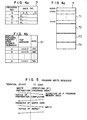
- Figs. 3a and 3b Several manners of setting program part memory areas will be explained with reference to Figs. 3a and 3b.
- the program part memory areas can be optionally provided by setting (writing) their attribute information in the table of the attribute information section 6.
- Figs. 3a to 3c are all directed to the initial writing.
- the corresponding items of attribute information are set so that the entire application program can be stored in the way of dividing it into plural program parts each having a previously set information length.
- the entire application program is first written in the program part memory area a.
- the program memory area is set to have a fixed length, regardless of the contents of the application program.
- the entire application program is previously stored in the program part memory area a which is a memory area of the entire application program.
- attribute information is written so that the program part a can be managed doubly as program parts b to g by writing the corresponding program parts as indicated by arrows for the partial change of the program.
- the program is stored by the sub-routine in the program part memory areas.
- the size of the program part memory area may be set at the size necessary to store the maximum one of the sub-routines.
- attribute information is previously written so that the program memory area a can be set doubly as only the program part areas b and c which are areas (e.g. area for table information) the rewrite of which is expected.
- the application program commonly has the constants employed internally or externally, the table for deciding the operation, etc. These are indicated internally in the program and hence the specification of the program can be changed to a certain degree by rewriting them. If the table information and the constants have only to be changed in rewriting the program, the program part memory areas may be rewritten.
- Fig. 3c is directed to the case of setting an area for e.g. table information, like Fig. 3b.
- the entire table information area is set as a program part memory area b.
- Information relative to specific controls of the table information is stored collectively in a program part memory area c.
- the sub-memory area can be further doubly set so that part of the table information can be further rewritten.
- a single application program need not be stored in the application program memory section 7 but plural different may be stored therein.
- Figs. 4a to 4c show one such an example.
- four application programs A, B, C and D (Fig. 4a) are stored in application program memory areas 71, 72, 73 and 74 of the application program memory section 7 (Fig. 4c).
- a program discrimination information section 9 is provided in the information memory part in order to discriminate the program memory areas for storing the program parts included in each application program.
- discrimination information for discriminating the application program and program part memory areas is inserted in a write instruction, it is possible to rewrite the program parts in each application program, in the same procedure and sequence as mentioned above, referring to the program discrimination information section 9 and attribute information memory section 61 (Fig. 4b). Additionally, specifying the application program in this example may be made by preparing a dedicated instruction without inserting the discrimination information in the write instruction. Moreover, if there are plural application programs, attribute information about the program may be provided for each program.
- Fig. 5 shows the procedure for rewriting program parts.
- a terminal device specifies, using a program area number, the program part memory area corresponding to the program part to be written and issues a write instruction thereof.
- An IC card after having received the write instruction, searches the specified program part memory area from the attribute information. Then, it acquires the base address and size of the pertinent program memory area for the preparation of write. After the completion of the preparation, the IC card informs the fact of the terminal device. In response to this, the terminal device prepares the transfer of the program to be written and transfers it to the IC card. The IC card performs the write of the program part after the receipt thereof or concurrently with the receipt.
- the IC card informs the terminal device of this fact, thereby completing the write.
- the terminal device has only to specify the program number corresponding to the pertinent program part whereby the IC card internally tests the finding of the area to be subjected to the write and the possibility of the write. The write is performed only if the IC card judges that the write can be made.
- the system program memory 4 may be provided in the information memory part 5.
- the attribute information about the program part memory areas may include the end address of each program memory area in place of the base address to specify the area by adding 1 to the end address of the previous area, or subtracting by 1 from the end address of the specified area. It may also include the end address and others in addition to the base address. Further, the attribute information should not be limited to such items but may be and management indicative of the reality of the program parts in the information memory part 5.
- the information memory part 5 may be composed of either a single memory element or plural elements as long as the application program memory section 7 is rewritable. Moreover, although the application program was made partially rewritable in the above embodiment, it may be any program as long as it can be executed by MPU 3. Additionally, address updating in the card reader writer for producing the program part for rewrite is ceased at the address corresponding to the end address for the program part memory area for rewrite.
Description
- The present invention relates to an IC card and a method for rewriting its program, and more particularly to a down-loadable IC card which is capable of rewriting its program quickly and a method for rewriting its processing program.
- 'IC cards' are now being used in a wide variety of applications. The IC cards issued in accordance with several kinds of transactions contain their individual data contents to be processed by different processing procedures. Therefore, the processing programs for the IC cards are peculiar to the terminals or host computers (hereinafter represented by terminals) in which they are employed.
- For this reason, there has been proposed 'down-load processing' IC cards in which from the terminals corresponding to several transactions including bank transaction, their corresponding processing programs are afterwards written into the IC cards.
- These IC cards include a rewritable non-volatile memory at their information memory part in which a processing program is stored; and thus if the operation of an IC card is desired to be changed, its program can be rewritten.
- However, such a system has the following problem. In performing the write or rewrite of a program for the IC card belonging to the above class, used are instructions dedicated to high speed transfer in which programs of about 1 to 8 K bytes are transferred each byte in place of block transfer in which blocks of about 10 to 80 bytes are transferred for each byte and provides a long overhead time. And also even if the program is to be partially rewritten, the IC card is adapted so that the program has to be wholly rewritten, which takes a long time for the rewrite of program.
- The program may include an application program and some parameters necessary for execution thereof. The parameters are constants, identification codes of the card and a user. Moreover, since a large amount of data must be transferred at a high speed in order to rewrite the program, the transfer error detection system becomes also complicated.
- JP-A-62-231,393 discloses an IC card containing a memory for storing data which is indexed, and is not concerned with the execution of program.
- FR-2,600,446 also discloses an IC card for storing indexed data.
- An aim of the present invention is to provide an IC card and a method for rewriting its program in which the rewrite can be done in a very short time only by transferring to the IC card a divided program including a part to be rewritten.
- Another aim of the present invention is to provide an IC card and a method for rewriting its program in which after a program is recorded in a plurality of divided programs in a memory area, if the size of the divided programs which are objects to be newly rewritten is made larger than that before the rewriting, they can be rewritten in accordance with their corresponding memory areas.
- Thus, according to the present invention there is provided a method for storing, rewriting and executing a program in an IC card having an input/output port for inputting a program to be down-loaded and outputting its processing result, a main storage area for storing data and programs, and a processor for sending the program input from the input/output port to said main storage area of the IC card, and a terminal for communicating commands to said IC card through said processor, the steps of the method comprising:
- storing the program comprised of a plurality of program parts in a plurality of corresponding sub-areas of a first portion of said main storage area of the IC card,
- storing a plurality of management information to identify each of the program parts stored in said sub-areas, each of said plurality of management information including a sub-area number for one of said program parts and a base address in a second portion of said main storage area of the IC card,
- sending a sub-area number corresponding to said program part to be rewritten from the terminal to the IC card,
- selecting a sub-area to be rewritten by referring to the management information based on said sub-area number,
- sending the program part to be rewritten,
- rewriting the contents of the selected sub-area with the sent program part, and
- executing sequentially said plurality of program parts in an order based on said management information.
- According to the present invention there is provided a system for storing, rewriting and executing a program in an IC card as set out in
claim 6. - The circuits arranged in the IC card include rewritable non-volatile memory means for storing the processing program to be executed by an ALU and management information for managing the areas where the processing program is stored in sub-areas of divisional programs; and means for writing, referring to the management information in accordance with the information specifying one or plural of the sub-areas input to the ALU, input programs in the sub-area(s).
- In order to manage a processing program stored in the rewritable non-volatile memory in the manner of being divided into plural programs constituting it, a region for storing attribute information, including the leading address and area length of each of the sub-areas where the program parts are stored, as management information indicative of the reality of the areas. It is possible to set attribute information optionally. The processing program with any size composed of the program parts can be stored. Moreover, the above sub-areas can be optionally selected afterwards. In rewriting the processing program, it is not rewritten by transferring a whole program to an IC card but is partially rewritten only as to the sub-area storing the contents to be changed in the rewritable non-volatile memory, referring to the management information including the top address and area length of that sub-area previously stored in the IC card (the management information may be rewritten before writing the program parts if necessary).
- In this way, in rewriting the processing program, only the program(s) which are desired to be rewritten in the processing program may be transferred to the IC card from the external device such as an IC card reader and writer, and therefore on the side of the IC card the entire program is not required to be rewritten so that the processing of rewriting the program can be efficiently carried out.
-
- Fig. 1 is a block diagram of the IC card according to one embodiment of the present invention;
- Fig. 2a is a table showing the relation between the entire processing program of the IC card and its divided program/data parts;
- Fig. 2b is a view showing the relation between areas for storing the divided program parts and their corresponding attribute information;
- Figs. 3a to 3c are memory maps showing several relations between the processing program and the divided program/data parts;
- Figs. 4a to 4c are views showing the relation between the attribute information about the program memory areas where a plurality of programs are stored, and their corresponding discrimination information; and
- Fig. 5 is a view for explaining one example of the communication sequence between an IC card and a terminal device.
- As seen from Fig. 1, an IC card 1 is composed of an I/
O part 2, an ALU or microprocessor unit (MPU) 3 and aninformation memory part 5 which may be rewritable non-volatile memory such as EEPROM. The I/O part 2 includes electrical contacts (not shown) on the surface of the IC card for inputting/outputting programs and for power supply. In place of the electrical contacts, electromagnetic induction may be adopted for downloading the program in the IC card. Theinformation memory part 5 is composed of an applicationprogram memory section 7, anattribute information section 6 for storing management information for the areas of the program parts into which the application program to be stored in theapplication program memory 7 is divided, anddata memory section 8 for storing several kinds of data. - MPU 3 includes a system program memory 4 (e.g. mask ROM) in which a
system program 4a for performing the hardware control of the IC card 1 is stored. By executing thesystem program 4a, MPU 3 performs the write/read of the program for the applicationprogram memory section 7 and the control of communication with terminal devices (e.g. IC card reader/writer incorporated therein). Moreover,MPU 3, by executing thesystem program 4a, performs the write of the attribute information transferred from an external device (the above terminal device) in the attributeinformation memory section 6 in accordance with an instruction transferred from the external device. As will be described later, the applicationprogram memory section 7 is managed in the manner of dividing it into a plurality of memory areas, corresponding to a plurality of program parts of the application program to be stored therein, in accordance with the attribute information stored in the attributeinformation memory section 6. - If the application program is to be down-loaded, it is executed for each of dividable program parts. Now it is assumed that the processing program is equally divided into program parts each with e.g. 32 bytes. However, the unit of division is not limited to 32 bytes but may be optionally selected.
- First, the attribute information (Fig. 2a) about each of the areas storing each program part (32 bytes) received at the I/
O part 2 is written in the attributeinformation memory section 6. The write of the attribute information is executed by activating the system program stored in thesystem program memory 4. - After the write of the attribute information, the write of the application program is performed in accordance with the sequence as shown in Fig. 5. First, a write instruction specifying the program part area to be subjected to the write using discrimination information provided in accordance with the divided program parts, i.e. the area numbers, is transferred to the IC card 1 from the terminal device (not shown). In response to the receipt of the write instruction,
MPU 3 of the IC card 1 aquires, in accordance with the above discrimination information, the top address, size, etc. of the pertinent program part memory area in the applicationprogram memory section 7 from the attribute information stored in the attributeinformation memory section 6 and prepares the write thereof. - After the completion of this preparation of write,
MPU 3 of the IC card 1 informs the terminal device of this fact through a data/control line 12 in accordance with thesystem program 4a. - Thus, data to be written (one of the divided program parts constituting a part of the processing program, i.e. 32 bytes) is transferred from terminal device. When received this write data, MPU 3 executes the write of the transferred program part (write data), in accordance with the
system program 4a, in the program part memory area (32 bytes) specified by the top or leading address and the size in the applicationprogram memory section 7 of theinformation memory part 5 of the IC card 1. Incidentally, if the memory area is fixed to 32 bytes, the above acquisition of the size of the memory area may be omitted. - After the completion of write of one data (32 bytes), discrimination information about the subsequent program part (32 bytes) is transferred from the terminal device in the same way. In accordance with the response on the side of the IC card 1, the program part (32 bytes) corresponding to the discrimination information is transferred from the terminal device. Then, this program part is stored in the program part memory area specified in accordance with the attribute information decided by the precedently transferred discrimination information, In this way, the program parts of one processing program are sequentially stored by 32 bytes. As a result, the entire processing program will be stored as a collection of the program data parts in the application
program memory section 7. - Fig. 2a shows the relation between the entire processing program thus stored (a in Fig. 3a) and its program parts (b to g in Fig. 3a), and Fig. 2b shows the relation between the memory areas for storing the program parts (Fig. 2b) and their attribute information (Fig. 2a). In this embodiment, as seen from Fig. 2b, the application
program memory section 7 is divided into n (n: integer of 2 or more)program memory areas 7a to 7n. Stored in plural memory areas (e.g. 7a to 7h) of the respective dividedmemory areas 7a to 7n are the program parts through the above write processing. In this case, the programpart memory areas 7i to 7n are vacant areas reserved for rewrite. The order of writing the program parts may be optional since the write is performed in accordance with the numbers of the sub-areas, i.e. items of discrimination information. - As seen from Fig. 2a, the attribute information is stored in a table form in the attribute
information memory section 6. Program area numbers are stored at the heads of the respective rows as information for discriminating the program areas for storing the program parts and further spaces for storing the base address and size for each row are provided. - The program area numbers, a, b, c, ... n in Fig. 2a correspond to the program
part memory areas - The application program in the case where it is managed in the program divided parts is executed in the sequence of the above program area numbers, namely in the sequence of a, b, c, ... n this embodiment. Therefore, initially, as shown in Fig. 2b, the sequence of the program area numbers a, b, c, ... n accord with the sequence of arranging the program parts. And even if the sequence is changed by rewriting any program part, any problem does not occur since the previous program area numbers are retained.
- Moreover, in the case where the processing program is not to be executed in the sequence of the numbers of program areas, information for specifying the sequence of connecting the program parts in the respective memory areas is previously stored in the
information memory section 5, or the program area number to be subsequently executed is previously stored at the end of the program part to be stored in each program area, thereby executing the application program composed of program parts the memory areas of which are discontinu- ously arranged. The sequence of executing the program parts may be stored in the attributeinformation memory section 6. - Now it is assumed that a shaded
portion 70 of theprogram part 7b is desired to be rewritten. In this case the rewrite of theprogram part 7b has only to be instructed from the terminal device, where the program parts relative to theprogram areas 7a and 7c to 7n are not required to be transferred. More specifically, if the rewrite portion is specified from the terminal device in terms of the discrimination information referring to the attribute information corresponding to theprogram memory area 7b,MPU 3, as in the case of write of the application program mentioned above, searches, acquires and accesses the attribute information relative to theprogram part 7b, referring to the discrimination information stored in theattribute memory section 6, in response to comparison between the description information and the attribute information, and writes the program part sent from the terminal device in the specified memory area. - Additionally, if the program part to be rewritten is smaller in size than the previous program part, the attribute information is not required to be changed since NOP is embedded in the remaining portion of the subarea. On the other hand, if the program data to be rewritten is in size larger than the previous program part, the overflowing portion is written in a
vacant area 7b′. And in executing the application program, added is an instruction of jumping to the top address (bbbb′ in Fig. 2b) of thearea 7b′ to execute the program part therein and jumping to the top address of the memory area subsequent to the area subjected to the rewrite. It is of course that the memory area of the program part to be stored in the vacant area is previously set by newly writing the attribute information thereof in the attributeinformation memory section 6. Otherwise, if the program part to be rewritten is larger in size than the previous program part, attribute information may be previously sent from the terminal device to register renewed base address and size for the same program area number in the attributeinformation memory section 6, thereby setting the area for storing in another vacant area of theinformation memory part 5. Then, the information in the memory area where the program part before the rewrite has been stored is cleared. - Several manners of setting program part memory areas will be explained with reference to Figs. 3a and 3b. In these cases, the program part memory areas can be optionally provided by setting (writing) their attribute information in the table of the
attribute information section 6. Incidentally, Figs. 3a to 3c are all directed to the initial writing. - In an embodiment of Fig. 3a, the corresponding items of attribute information are set so that the entire application program can be stored in the way of dividing it into plural program parts each having a previously set information length. In initially writing the application program, the entire application program is first written in the program part memory area a. In this case, the program memory area is set to have a fixed length, regardless of the contents of the application program. In this way, the entire application program is previously stored in the program part memory area a which is a memory area of the entire application program. Thereafter, attribute information is written so that the program part a can be managed doubly as program parts b to g by writing the corresponding program parts as indicated by arrows for the partial change of the program.
- In the case where the application program can be divided by sub-routines as function units, the program is stored by the sub-routine in the program part memory areas. In this case, the size of the program part memory area may be set at the size necessary to store the maximum one of the sub-routines.
- In an embodiment of Fig. 3b, attribute information is previously written so that the program memory area a can be set doubly as only the program part areas b and c which are areas (e.g. area for table information) the rewrite of which is expected. The application program commonly has the constants employed internally or externally, the table for deciding the operation, etc. These are indicated internally in the program and hence the specification of the program can be changed to a certain degree by rewriting them. If the table information and the constants have only to be changed in rewriting the program, the program part memory areas may be rewritten.
- Fig. 3c is directed to the case of setting an area for e.g. table information, like Fig. 3b. In this case, the entire table information area is set as a program part memory area b. Information relative to specific controls of the table information is stored collectively in a program part memory area c. In this way, the sub-memory area can be further doubly set so that part of the table information can be further rewritten.
- In all of the above cases, if the program part to be rewritten in the program memory area a is comparatively large, a program instructing the jump to another program part memory area, which is a rewrite destination, is written. Thus, the execution sequence is shifted to the other program part stored in a vacant memory area of the application
program memory section 7, thereby executing the entire application program. - Moreover, a single application program need not be stored in the application
program memory section 7 but plural different may be stored therein. Figs. 4a to 4c show one such an example. In this example, four application programs A, B, C and D (Fig. 4a) are stored in applicationprogram memory areas - If, prior to executing the write, discrimination information for discriminating the application program and program part memory areas is inserted in a write instruction, it is possible to rewrite the program parts in each application program, in the same procedure and sequence as mentioned above, referring to the program discrimination information section 9 and attribute information memory section 61 (Fig. 4b). Additionally, specifying the application program in this example may be made by preparing a dedicated instruction without inserting the discrimination information in the write instruction. Moreover, if there are plural application programs, attribute information about the program may be provided for each program.
- Fig. 5 shows the procedure for rewriting program parts. A terminal device specifies, using a program area number, the program part memory area corresponding to the program part to be written and issues a write instruction thereof. An IC card, after having received the write instruction, searches the specified program part memory area from the attribute information. Then, it acquires the base address and size of the pertinent program memory area for the preparation of write. After the completion of the preparation, the IC card informs the fact of the terminal device. In response to this, the terminal device prepares the transfer of the program to be written and transfers it to the IC card. The IC card performs the write of the program part after the receipt thereof or concurrently with the receipt. After the completion of the write, the IC card informs the terminal device of this fact, thereby completing the write. As understood from the above description, the terminal device has only to specify the program number corresponding to the pertinent program part whereby the IC card internally tests the finding of the area to be subjected to the write and the possibility of the write. The write is performed only if the IC card judges that the write can be made.
- In the arrangement of the IC card shown in Fig. 1, the
system program memory 4 may be provided in theinformation memory part 5. Moreover, the attribute information about the program part memory areas may include the end address of each program memory area in place of the base address to specify the area by adding 1 to the end address of the previous area, or subtracting by 1 from the end address of the specified area. It may also include the end address and others in addition to the base address. Further, the attribute information should not be limited to such items but may be and management indicative of the reality of the program parts in theinformation memory part 5. - The
information memory part 5 may be composed of either a single memory element or plural elements as long as the applicationprogram memory section 7 is rewritable. Moreover, although the application program was made partially rewritable in the above embodiment, it may be any program as long as it can be executed byMPU 3. Additionally, address updating in the card reader writer for producing the program part for rewrite is ceased at the address corresponding to the end address for the program part memory area for rewrite.
Claims (6)
- A method for storing, rewriting and executing a program in an IC card having an input/output port (2) for inputting a program to be down-loaded and outputting its processing result, a main storage area (5) for storing data and programs, and a processor (3) for sending the program input from the input/output port to said main storage area of the IC card, and a terminal for communicating commands to said IC card through said processor, the steps of the method comprising:storing the program comprised of a plurality of program parts in a plurality of corresponding sub-areas of a first portion (7) of said main storage area of the IC card,storing a plurality of management information to identify each of the program parts stored in said sub-areas, each of said plurality of management information including a sub-area number for one of said program parts and a base address in a second portion (6) of said main storage area (5) of the IC card,sending a sub-area number corresponding to a program part to be rewritten from the terminal to the IC card,selecting a sub-area to be rewritten by referring to the management information based on said sub-area number,sending the program part to be rewritten,rewriting the contents of the selected sub-area with the sent program part, andexecuting sequentially said plurality of program parts in an order based on said management information.
- A method according to claim 1, further comprising the steps of, if a selected program part to be rewritten exceeds the capacity of the sub-area previously occupied by an original program part, rewriting a base address of the management information corresponding to said original program part with an address of another vacant sub-area and automatically storing said selected program part into said other vacant sub-area of said plurality of sub-areas in said main storage of the IC card.
- A method according to claim 1 or 2, wherein each said management information also includes the size of the sub-area in correspondence to said sub-area number and said base address included in said management information.
- A method according to claim 1, 2 or 3, further comprising the step of:
when the program part for rewrite exceeds the capacity of the sub-area where an original program part has been stored, providing an instruction of jumping to the address of a vacant sub-area in the program part and thereafter jumping to the vacant sub-area. - A method according to claim 1, 2, 3 or 4 wherein the memory capacity of the sub-areas is fixed at 32 bytes.
- A system for storing, rewriting and executing a program in an IC card (1) having an input/output port (2) for inputting a program to be down-loaded and outputting its processing result, a main storage area (7) for storing data and programs, and a processor (3) for sending the program input from the input/output port to said main storage area of the IC card, and a terminal for communicating commands to said IC card through said processor, the system comprising:means (3) for storing the program comprised of a plurality of program parts in a plurality of corresponding sub-areas of a first portion (7) of said main storage area of the IC card,means (3) for storing a plurality of management information to identify each of the program parts stored in said plurality of sub-areas, each of said plurality of management information including a sub-area number for one of said sub-areas and a base address in a second portion (6) of said main storage area of the IC card,means (3) for sending a sub-area number corresponding to a program part to be rewritten from the terminal to the IC card,means for selecting a sub-area to be rewritten by referring to the management information based on said sub-area number,means (3) for sending the program part to be rewritten,means for rewriting contents of the selected sub-area with the sent program part, andmeans for executing sequentially said plurality of program parts in an order based on said management information.
Applications Claiming Priority (4)
| Application Number | Priority Date | Filing Date | Title |
|---|---|---|---|
| JP63201218A JPH0250786A (en) | 1988-08-12 | 1988-08-12 | Ic card and its program rewriting system |
| JP201218/88 | 1988-08-12 | ||
| JP201219/88 | 1988-08-12 | ||
| JP63201219A JPH0250787A (en) | 1988-08-12 | 1988-08-12 | Ic card and its program rewriting system |
Publications (3)
| Publication Number | Publication Date |
|---|---|
| EP0354793A2 EP0354793A2 (en) | 1990-02-14 |
| EP0354793A3 EP0354793A3 (en) | 1990-12-27 |
| EP0354793B1 true EP0354793B1 (en) | 1996-10-23 |
Family
ID=26512662
Family Applications (1)
| Application Number | Title | Priority Date | Filing Date |
|---|---|---|---|
| EP19890308141 Revoked EP0354793B1 (en) | 1988-08-12 | 1989-08-10 | IC card and method for rewriting its program |
Country Status (2)
| Country | Link |
|---|---|
| EP (1) | EP0354793B1 (en) |
| DE (2) | DE68927361T4 (en) |
Cited By (11)
| Publication number | Priority date | Publication date | Assignee | Title |
|---|---|---|---|---|
| US6164549A (en) | 1997-05-15 | 2000-12-26 | Mondex International Limited | IC card with shell feature |
| US6220510B1 (en) | 1997-05-15 | 2001-04-24 | Mondex International Limited | Multi-application IC card with delegation feature |
| US6328217B1 (en) | 1997-05-15 | 2001-12-11 | Mondex International Limited | Integrated circuit card with application history list |
| US6385723B1 (en) | 1997-05-15 | 2002-05-07 | Mondex International Limited | Key transformation unit for an IC card |
| US6488211B1 (en) | 1997-05-15 | 2002-12-03 | Mondex International Limited | System and method for flexibly loading in IC card |
| US6575372B1 (en) | 1997-02-21 | 2003-06-10 | Mondex International Limited | Secure multi-application IC card system having selective loading and deleting capability |
| US6736325B1 (en) | 1998-01-22 | 2004-05-18 | Mondex International Limited | Codelets |
| US6742120B1 (en) | 1998-02-03 | 2004-05-25 | Mondex International Limited | System and method for controlling access to computer code in an IC card |
| US6761319B2 (en) | 1998-01-22 | 2004-07-13 | Mondex International Limited | Configuration of IC card |
| US7669055B2 (en) | 1997-02-21 | 2010-02-23 | Multos Limited | Key transformation unit for a tamper resistant module |
| US8794516B2 (en) | 1999-10-25 | 2014-08-05 | Smartflash, LLC | Data storage and access systems |
Families Citing this family (6)
| Publication number | Priority date | Publication date | Assignee | Title |
|---|---|---|---|---|
| JPH03240127A (en) * | 1990-02-17 | 1991-10-25 | Hitachi Maxell Ltd | Program control system |
| US6230267B1 (en) | 1997-05-15 | 2001-05-08 | Mondex International Limited | IC card transportation key set |
| DE69820353T2 (en) * | 1997-08-01 | 2004-09-02 | Kabushiki Kaisha Toshiba, Kawasaki | Smart card issuing system and method |
| AUPP274098A0 (en) * | 1998-04-01 | 1998-04-30 | Chip Application Technologies Limited | Data carrying device and systems for use therewith |
| DE10040974A1 (en) | 2000-08-22 | 2002-03-14 | Giesecke & Devrient Gmbh | Virtual stack enlargement method for portable data carrier read/write memory has stack divided into stack segments with transfer of stack segment contents to further storage medium |
| FR2835628A1 (en) * | 2002-02-01 | 2003-08-08 | Schlumberger Systems & Service | MANAGEMENT OF THE UPDATE OF INFORMATION ENCODED IN MEMORY |
Family Cites Families (2)
| Publication number | Priority date | Publication date | Assignee | Title |
|---|---|---|---|---|
| US4829169A (en) * | 1985-07-01 | 1989-05-09 | Toppan Moore Company, Inc. | IC card having state marker for record access |
| JP2537199B2 (en) * | 1986-06-20 | 1996-09-25 | 株式会社東芝 | IC card |
-
1989
- 1989-08-10 DE DE1989627361 patent/DE68927361T4/en not_active Expired - Lifetime
- 1989-08-10 DE DE1989627361 patent/DE68927361D1/en not_active Expired - Fee Related
- 1989-08-10 EP EP19890308141 patent/EP0354793B1/en not_active Revoked
Cited By (21)
| Publication number | Priority date | Publication date | Assignee | Title |
|---|---|---|---|---|
| US7730312B2 (en) | 1997-02-21 | 2010-06-01 | Multos Limted | Tamper resistant module certification authority |
| US7730311B2 (en) | 1997-02-21 | 2010-06-01 | Multos Limited | Key transformation unit for a tamper resistant module |
| US7734923B2 (en) | 1997-02-21 | 2010-06-08 | Multos Limited | Key transformation unit for a tamper resistant module |
| US7689826B2 (en) | 1997-02-21 | 2010-03-30 | Multos Limited | Flexibly loading a tamper resistant module |
| US7669055B2 (en) | 1997-02-21 | 2010-02-23 | Multos Limited | Key transformation unit for a tamper resistant module |
| US6575372B1 (en) | 1997-02-21 | 2003-06-10 | Mondex International Limited | Secure multi-application IC card system having selective loading and deleting capability |
| US6659354B2 (en) | 1997-02-21 | 2003-12-09 | Mondex International Limited | Secure multi-application IC card system having selective loading and deleting capability |
| US7730310B2 (en) | 1997-02-21 | 2010-06-01 | Multos Limited | Key transformation unit for a tamper resistant module |
| US7707408B2 (en) | 1997-02-21 | 2010-04-27 | Multos Limited | Key transformation unit for a tamper resistant module |
| US7702908B2 (en) | 1997-02-21 | 2010-04-20 | Multos Limited | Tamper resistant module certification authority |
| US6328217B1 (en) | 1997-05-15 | 2001-12-11 | Mondex International Limited | Integrated circuit card with application history list |
| US6488211B1 (en) | 1997-05-15 | 2002-12-03 | Mondex International Limited | System and method for flexibly loading in IC card |
| US6385723B1 (en) | 1997-05-15 | 2002-05-07 | Mondex International Limited | Key transformation unit for an IC card |
| US6742715B2 (en) | 1997-05-15 | 2004-06-01 | Mondex International Limited | System and method for flexibly loading an IC card |
| US6164549A (en) | 1997-05-15 | 2000-12-26 | Mondex International Limited | IC card with shell feature |
| US6220510B1 (en) | 1997-05-15 | 2001-04-24 | Mondex International Limited | Multi-application IC card with delegation feature |
| US6736325B1 (en) | 1998-01-22 | 2004-05-18 | Mondex International Limited | Codelets |
| US6761319B2 (en) | 1998-01-22 | 2004-07-13 | Mondex International Limited | Configuration of IC card |
| US6742120B1 (en) | 1998-02-03 | 2004-05-25 | Mondex International Limited | System and method for controlling access to computer code in an IC card |
| US8794516B2 (en) | 1999-10-25 | 2014-08-05 | Smartflash, LLC | Data storage and access systems |
| US9471910B2 (en) | 1999-10-25 | 2016-10-18 | Smartflash, LLC | Data storage and access systems |
Also Published As
| Publication number | Publication date |
|---|---|
| EP0354793A2 (en) | 1990-02-14 |
| DE68927361T2 (en) | 1997-03-27 |
| DE68927361D1 (en) | 1996-11-28 |
| EP0354793A3 (en) | 1990-12-27 |
| DE68927361T4 (en) | 1999-11-04 |
Similar Documents
| Publication | Publication Date | Title |
|---|---|---|
| US5276903A (en) | Method for rewriting partial program data in an IC card and apparatus therefor | |
| EP0354793B1 (en) | IC card and method for rewriting its program | |
| EP0451936B1 (en) | Program control system for portable data storage device | |
| US5093785A (en) | Portable electronic device with memory having data pointers and circuitry for determining whether a next unwritten memory location exist | |
| US6742715B2 (en) | System and method for flexibly loading an IC card | |
| EP0271495B1 (en) | Ic card system | |
| JP2914360B2 (en) | External storage device and data processing method | |
| US4983816A (en) | Portable electronic device | |
| WO1998052153A2 (en) | Ic card with shell feature | |
| US7017825B2 (en) | IC card and data processing method therefor | |
| JPH06282471A (en) | File control system | |
| US5159183A (en) | Ic card | |
| US6286757B1 (en) | Portable electronic apparatus | |
| US6301622B1 (en) | Computer system having identification data and method for transferring identification data to computer | |
| EP0973127B1 (en) | IC card, IC card processing system, and IC card processing method | |
| JP3088866B2 (en) | IC card | |
| EP0863513A2 (en) | Method of writing data into memory with finite guaranteed write number of times and device for writing data into such memory | |
| JP7005934B2 (en) | Electronic information storage medium, IC card, data transmission method, data writing method, data transmission program and data writing program | |
| EP1384197B1 (en) | Method of manufacturing smart cards | |
| EP1301929B1 (en) | Secure writing of data | |
| JPH0250786A (en) | Ic card and its program rewriting system | |
| EP1804189A2 (en) | Recording method, recorder and IC card | |
| JP3168572B2 (en) | IC card with CPU runaway detection function | |
| WO1999038131A1 (en) | Codelets | |
| KR20020030797A (en) | Method and device for assembling circuit carriers arranged in a pick and place machine |
Legal Events
| Date | Code | Title | Description |
|---|---|---|---|
| PUAI | Public reference made under article 153(3) epc to a published international application that has entered the european phase |
Free format text: ORIGINAL CODE: 0009012 |
|
| AK | Designated contracting states |
Kind code of ref document: A2 Designated state(s): DE FR GB |
|
| PUAL | Search report despatched |
Free format text: ORIGINAL CODE: 0009013 |
|
| AK | Designated contracting states |
Kind code of ref document: A3 Designated state(s): DE FR GB |
|
| 17P | Request for examination filed |
Effective date: 19910502 |
|
| 17Q | First examination report despatched |
Effective date: 19930325 |
|
| GRAG | Despatch of communication of intention to grant |
Free format text: ORIGINAL CODE: EPIDOS AGRA |
|
| GRAH | Despatch of communication of intention to grant a patent |
Free format text: ORIGINAL CODE: EPIDOS IGRA |
|
| GRAH | Despatch of communication of intention to grant a patent |
Free format text: ORIGINAL CODE: EPIDOS IGRA |
|
| GRAA | (expected) grant |
Free format text: ORIGINAL CODE: 0009210 |
|
| AK | Designated contracting states |
Kind code of ref document: B1 Designated state(s): DE FR GB |
|
| ET | Fr: translation filed | ||
| REF | Corresponds to: |
Ref document number: 68927361 Country of ref document: DE Date of ref document: 19961128 |
|
| PLBI | Opposition filed |
Free format text: ORIGINAL CODE: 0009260 |
|
| PLBF | Reply of patent proprietor to notice(s) of opposition |
Free format text: ORIGINAL CODE: EPIDOS OBSO |
|
| 26 | Opposition filed |
Opponent name: GIESECKE & DEVRIENT GMBH Effective date: 19970723 |
|
| PLBF | Reply of patent proprietor to notice(s) of opposition |
Free format text: ORIGINAL CODE: EPIDOS OBSO |
|
| PLBF | Reply of patent proprietor to notice(s) of opposition |
Free format text: ORIGINAL CODE: EPIDOS OBSO |
|
| PLBO | Opposition rejected |
Free format text: ORIGINAL CODE: EPIDOS REJO |
|
| APAC | Appeal dossier modified |
Free format text: ORIGINAL CODE: EPIDOS NOAPO |
|
| APAE | Appeal reference modified |
Free format text: ORIGINAL CODE: EPIDOS REFNO |
|
| APAC | Appeal dossier modified |
Free format text: ORIGINAL CODE: EPIDOS NOAPO |
|
| PGFP | Annual fee paid to national office [announced via postgrant information from national office to epo] |
Ref country code: FR Payment date: 20010523 Year of fee payment: 13 |
|
| PGFP | Annual fee paid to national office [announced via postgrant information from national office to epo] |
Ref country code: GB Payment date: 20010808 Year of fee payment: 13 |
|
| PGFP | Annual fee paid to national office [announced via postgrant information from national office to epo] |
Ref country code: DE Payment date: 20011030 Year of fee payment: 13 |
|
| REG | Reference to a national code |
Ref country code: GB Ref legal event code: IF02 |
|
| PG25 | Lapsed in a contracting state [announced via postgrant information from national office to epo] |
Ref country code: GB Free format text: LAPSE BECAUSE OF NON-PAYMENT OF DUE FEES Effective date: 20020810 |
|
| PG25 | Lapsed in a contracting state [announced via postgrant information from national office to epo] |
Ref country code: DE Free format text: LAPSE BECAUSE OF NON-PAYMENT OF DUE FEES Effective date: 20030301 |
|
| GBPC | Gb: european patent ceased through non-payment of renewal fee |
Effective date: 20020810 |
|
| REG | Reference to a national code |
Ref country code: FR Ref legal event code: ST |
|
| APBU | Appeal procedure closed |
Free format text: ORIGINAL CODE: EPIDOSNNOA9O |
|
| RDAF | Communication despatched that patent is revoked |
Free format text: ORIGINAL CODE: EPIDOSNREV1 |
|
| RDAG | Patent revoked |
Free format text: ORIGINAL CODE: 0009271 |
|
| STAA | Information on the status of an ep patent application or granted ep patent |
Free format text: STATUS: PATENT REVOKED |
|
| 27W | Patent revoked |
Effective date: 20030724 |
|
| APAH | Appeal reference modified |
Free format text: ORIGINAL CODE: EPIDOSCREFNO |
|
| PG25 | Lapsed in a contracting state [announced via postgrant information from national office to epo] |
Ref country code: FR Free format text: LAPSE BECAUSE OF NON-PAYMENT OF DUE FEES Effective date: 20020831 |