EP0229932A2 - High-capacity memory for multiprocessor systems - Google Patents
High-capacity memory for multiprocessor systems Download PDFInfo
- Publication number
- EP0229932A2 EP0229932A2 EP86116470A EP86116470A EP0229932A2 EP 0229932 A2 EP0229932 A2 EP 0229932A2 EP 86116470 A EP86116470 A EP 86116470A EP 86116470 A EP86116470 A EP 86116470A EP 0229932 A2 EP0229932 A2 EP 0229932A2
- Authority
- EP
- European Patent Office
- Prior art keywords
- memory
- fact
- bits
- agents
- address
- Prior art date
- Legal status (The legal status is an assumption and is not a legal conclusion. Google has not performed a legal analysis and makes no representation as to the accuracy of the status listed.)
- Granted
Links
Images
Classifications
-
- G—PHYSICS
- G06—COMPUTING; CALCULATING OR COUNTING
- G06F—ELECTRIC DIGITAL DATA PROCESSING
- G06F12/00—Accessing, addressing or allocating within memory systems or architectures
- G06F12/14—Protection against unauthorised use of memory or access to memory
- G06F12/1458—Protection against unauthorised use of memory or access to memory by checking the subject access rights
- G06F12/1483—Protection against unauthorised use of memory or access to memory by checking the subject access rights using an access-table, e.g. matrix or list
-
- G—PHYSICS
- G06—COMPUTING; CALCULATING OR COUNTING
- G06F—ELECTRIC DIGITAL DATA PROCESSING
- G06F12/00—Accessing, addressing or allocating within memory systems or architectures
- G06F12/02—Addressing or allocation; Relocation
- G06F12/0223—User address space allocation, e.g. contiguous or non contiguous base addressing
- G06F12/0284—Multiple user address space allocation, e.g. using different base addresses
-
- G—PHYSICS
- G06—COMPUTING; CALCULATING OR COUNTING
- G06F—ELECTRIC DIGITAL DATA PROCESSING
- G06F12/00—Accessing, addressing or allocating within memory systems or architectures
- G06F12/02—Addressing or allocation; Relocation
- G06F12/0223—User address space allocation, e.g. contiguous or non contiguous base addressing
- G06F12/0292—User address space allocation, e.g. contiguous or non contiguous base addressing using tables or multilevel address translation means
Definitions
- the present invention relates to a high-capacity memory accessible by a number of external agents (particularly processors), having a data capacity possibly exceeding the addressing capacity of each of the said agents, and particularly suitable for use on multiprocessor systems.
- a need is generally acknowledged for combining high computing power with the ability to handle large streams of in-coming and out-going data, particularly in applications involving complex real-time processing (e.g. image processing, pattern and voice recognition, artifical intelligence and scientific computation in general).
- complex real-time processing e.g. image processing, pattern and voice recognition, artifical intelligence and scientific computation in general.
- the formation of high-computing-power multiprocessor systems poses various problems, including addressing capacity of the memories, and rapid data transfer between different memory groups.
- the aim of the present invention is to provide a high-capacity memory which may be used to advantage on multiprocessor systems, which is accessible by various agents (processors) at different ports, and whereby, for each agent, each word "segment" into which the memory is conceptually divided may be assigned "visibility or non-visibility” by the said agent, access rights (read-only, read/ write, perform-only, etc.), and random positioning (addressing) in the agent address space, for the purpose of: exceeding the addressing limits of the agent by dynamically assigning, to part of the segments, the logic function of a "secondary memory” logically equivalent to a disk, or the function of a direct-access main memory, which, though logically equivalent to transferring data from the main to the secondary memory or vice versa, involves no physical transfer of data, which may thus be performed extremely rapidly and regardless of segment size;
- a high-capacity memory characterised by the fact that it is accessible by at least two external agents, and that it comprises means for addressing the said memory independently of the addresses emitted by each of the said agents.
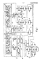
- Fig.1 shows a block diagram of a multiprocessor system to which is applied the memory according to the present invention.
- the major parts on the said multiprocessor system relative to application of the memory according to the present invention will now be described in detail, the said system itself being described in Italian Patent Application entitled “Multiple-Hierarchical-Level Multiprocessor System” filed on the same date by the present Applicant, and the content of which is incorporated herein solely by way of reference as required.
- the said multiprocessor system presents a common bus structure and is divided into a number of regions 10, each composed of a group of families 11.
- Each family consists of a number of processors accessible directly by a common bus 12 (family bus), and all the families 11 in one region 10 are, in turn, accessible directly via a common bus 13 (region bus).
- the processors are connected tightly, i.e. affording direct visibility of the entire memory in the region, whereas different regions 10 are connected loosely, i.e. via messages exchanged via units 14 connected by lines 15.
- System monitoring and supervision functions are conveniently performed by a special region 10' connected, via units 14, to all the other regions 10 on the system, and, via modules described in more detail later on, to an external computer 16.
- Each family 11 comprises : a monoprocessor module 17 (PI) connected via lines 19 and 20 to family bus 12 and region bus 13 respectively; a number of multiprocessor modules 18 (PN) connected via lines 19' to family bus 12 only; a high-capacity memory block 22 (HCSM) according to the present invention and conveniently of 8 Megabytes; and an input/output block 23 (1/0) for receiving and transmitting data from and to the application environment of the multiprocessor system.
- Memory block 22 is connected, via lines 24 and 25, to family bus and region bus 13 respectively, whereas block 23 is connected solely to family bus 12.
- Region bus 13 may also be connected to input/output blocks 26 (I/0) for communicating with peripherals.
- Monoprocessor module 17 (P1) thus provides for linking the two (family and region) hierarchical levels.
- monitoring region 10' is connected to an external computer 16 via unit 14 (IRCU), in turn, connected to a TTL-differential signal converting unit 115 (TDC) connected to computer 16 via a single or two parallel-connected interface modules 116.
- the said modules 116 may be standard DMA interfaces, e.g. DR11-W, in the case of a VAX11/750 external computer 16 connection.
- the various region 13 and family 12 buses present roughly the same characteristics : they support master, slave, and master/slave modules, and carry 5 groups of signals (address and status, data, control, error, and arbitration). Both provide for 32-bit data transfer at a speed, in burst mode, of over 10 Megabytes/second.
- a 32-bit bus size enables the use of 32-bit processors. Even when using 16-bit processors, however, characteristics may be available for exploiting the said bus size for speeding up data transfer.
- all the memories accessible by the buses are parallel-organized over 32 bits.
- the multiprocessor system therefore comprises a number of the said regions 10 interconnected via high-speed parallel connections.
- the said multiprocessor system may be defined, at this higher level, as a region network, the geometry of which may be defined as required for best catering for a given application. Furthermore, by connecting monitoring region 10' to external computer 16, the entire system benefits from the programs and peripheral devices of ready-made commercial machines.
- Each region 10 therefore consists of a number of the said families 11, and shares a common memory address space and a common bus 13. To be more precise, a common region address space of 7 Megabytes may be divided into subspaces assigned to memory blocks or processing modules connected to the said region bus 13. These processing units have access to reciprocal memory subspaces via region bus 13.
- each family 11 consists of a group of processing modules sharing a common memory address space and a common bus 12. As in the case of region 10, a family memory space of 8 Megabytes is divided into local (though not private) subspaces for the various processor modules, which are allowed access to reciprocal memory spaces via family bus 12.
- Module PI is allowed visibility of both the address space of its own family (1 P1 per family) and the region address space to which may be connected a number of families (conveniently 32, for example). PI also avails itself of the two high-capacity family 12 and region 13 buses, and all the hardware characteristics already described.
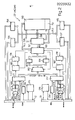
- Block 22 is designed for high- efficiency exchange of large amounts of data between the two environments (family and region).
- Memory block 22 presents a memory array 150 with a section 151 for control bits exchanged with a logic error detecting and correcting block 152.
- the read or write data in memory 150 goes to lines 153 (conveniently 32-bit) connected to two write data registers 154 and 155, respectively connected to family bus 12 and region bus 13, and to two read data registers 156 and 157 also connected respectively to family bus 12 and region bus 13.
- the data exchanged with memory 150 also goes, via lines 158, to logic block 152, which is also connected, via a read or write control line 159, to line 153, and, via an error signal line 160, to a block 161 for arbitrating requests, controlling the double (family-region) port and timing the control signals of memory 150.
- the said block 161 supplies memory 150 with address signals 163 (RAS/CAS/ADDRESS).
- Region bus 13 is also connected in the same manner to functionally equivalent blocks indicated using the same numbers plus a '.
- the status output of latch 171 goes to a status decoding and cycle request generating block 180 connected to block 178 and block 161.
- the status output of latch 171' is connected in the same manner.
- the address outputs (bits 0 to 22) of latches 171 and 171' go to the inputs of a multiplexer 182 controlled by block 161 and the output of which goes directly (via only conjunction or disjunction block 183) or via pipeline 184, to the address input of arbitration block 161 which also controls logic blocks 178 and 178'.
- the maximum capacity of memory block 22 is 8 Megabytes, divided into 128 segments of 64 Kbytes each.
- the said memory 22 is visible by both family bus 12 and region bus 13, and, as memory capacity is greater than the address space available for each bus, the present invention provides for a mapping mechanism enabling both buses to exceed the physical 8 Mbyte limit.
- the memory is organized on a 32-bit word length (double word) and permits 32-bit (double word), 16-bit (word) and 8-bit (byte) read and write access.
- the two (family and region) memory access ports present two identical, independent mapping systems.
- the logic of the said systems provides for dividing the 8 Mbyte total into 128 segments of 64 Kbytes each, each of which segments may be shifted to any point within the physical address space (within 64 K limits).
- a physical address is assigned to a given segment by writing the segment number into the mapping register of the relative address.
- the mapping registers are grouped into 128-word RAM memory block 168 and 168'. In normal read and write cycles of memory array 150, the address from the family and region bus is composed of two parts :
- the mapping mechanism on the present invention provides for installing a number of memories 22 (HCSM) on the same region or family bus, as well as for enabling exclusive visibility of the memories by the region or the family. Furthermore, a segment shift involves no data transfer, simply the modification of a mapping register on block 168 or 168'.
- HCSM a number of memories 22
- the memory 22 control program initializes and modifies the family and region mapping RAMs 168 and 168' by obtain ing access to a specific (switch-selectable) portion of the family and region I/O space.
- Control registers 176 and 176' are provided with a bit for preventing access to memory 22 until the control program has initialized mapping RAMs 168 and 168'.
- HCSM memory block 22
- pipeline address generation 8-, 16-, 32-bit data transfer
- possibility of discontinuous or locked access 8-, 16-, 32-bit data transfer
- memory 22 is a double-port type, which means provision must be made for controlling the conflicting priority of fully asynchronous in-coming requests from region bus 13 and family bus 12.
- the temporary address storage problem is overcome by storing the addresses in latches 171 and 171'.
- Status (e.g. DOUBLE WORD) signal decoding supplies dynamic memory control block 161 with information concerning the type of cycle requested.
- the same block 161 also provides for request synchronization and arbitration, as well as for ensuring "locked" data transfer.
- two registers 154 and 155 (one for each bus) have been provided for accommodating input data and so terminating the bus cycle in as short a time as possible. Random read cycles are penalized by the access time of dynamic memory 150, to which must be added the delay introduced by logic error detecting and correcting block 152, and request synchronization time.
- Performance is considerably improved in the case of sequential and locked access, whereby the address of the memory location to be requested in the next cycle may be "forecast", and pipelining logic activated for withdrawing the data item in advance and so ensuring it is made immediately available when requested by the master. In this case also, therefore, the bus is engaged for a minimum length of time.
- the data item withdrawn from memory 150 is, in any case, accommodated in two separate registers 156 and 157 (one for each bus), for preventing possible interference between cycles activated by different buses.
- Memory array 150 is parallel-organized over 32 bits for fully exploiting the transfer capacity of the memory according to the present invention.
- HCSM logic of module 22
- the said HCSM module may also be formed in 6, 4, 2 Mbytes, with or without error detection and correction via block 152.
- the high-capacity memory may comprise a main memory array block 150 of 2 N words, accessible by p different agents (in particular, processors) at p different ports, and divided conceptually into 2 N-K segments of 2 K words each.
- the physical address of any one word on block 150 therefore consists of N bits, of which N-K indicate the segment, and K the word within the segment.
- the characteristic of the present invention enabling independent addressing of the memory in the various agent address spaces is achieved simply and cheaply by inserting, on the address route of each port, a small mapping and characterisation memory similar to memories 168 and 168' in Fig.2 and consisting of a number of words equal to the number of words addressable by the agent divided by the segment size 2 K .
- the said words have K-K bits (for physical addressing of the segments on memory array 150), plus visibility, access right and any other characterisation bits.
- the N address bits for the memory array are therefore obtained from the K least significant address bits supplied directly by the agent, and from the (N-K) segment address bits obtained from the mapping memory.
- the said N agent address bits are sent to the memory array via an agent address scanning block (similar to block 182 in Fig.2) controlled by a logic control and arbitration block (similar to block 161 in Fig.2) which receives (among other things) the visibility bits at the output of the mapping and characterisation memory, and agent access control signals, as already described with reference to Fig.2.
- agent address scanning block similar to block 182 in Fig.2
- logic control and arbitration block similar to block 161 in Fig.2 which receives (among other things) the visibility bits at the output of the mapping and characterisation memory, and agent access control signals, as already described with reference to Fig.2.
- the agent will thus be unable to see, at the same time, more than 256 of the 512 (2 N-K ) memory segments, it is possible to determine arbitrarily which of the said segments will be made visible at any given time, and for which addresses emitted by the agent, via a small 256-word mapping and characterisation memory (usually having a different word length from the memory array!).
- the 16 least significant bits are sent directly to the memory array, and the 8 most significant bits to the small mapping memory which, in the event a memory array segment is to be assigned to that particular address, emits the corresponding 9 segment address bits, plus a visibility bit and any other segment characterisation bits.
- this can be done by simply changing the content of word 2E on the characterisation memory from 1A3 to OF5. This corresponds logically to transferring 2 16 words from the primary to the secondary memory and vice versa, but in a performance time measurable in microseconds.
- the memory according to the present invention provides for exceeding the addressing limits of each agent; secondly, for dynamically switching memory data from one agent to another, thus achieving the equivalent of a data transfer at practically infinite speed; and, finally, for dynamically creating areas common to different agents, possibly with different access rights.
- changes may be made to the embodiment of the memory described and illustrated herein without, however, departing from the scope of the present invention.
Abstract
Description
- The present invention relates to a high-capacity memory accessible by a number of external agents (particularly processors), having a data capacity possibly exceeding the addressing capacity of each of the said agents, and particularly suitable for use on multiprocessor systems. A need is generally acknowledged for combining high computing power with the ability to handle large streams of in-coming and out-going data, particularly in applications involving complex real-time processing (e.g. image processing, pattern and voice recognition, artifical intelligence and scientific computation in general). The formation of high-computing-power multiprocessor systems poses various problems, including addressing capacity of the memories, and rapid data transfer between different memory groups.
- The aim of the present invention is to provide a high-capacity memory which may be used to advantage on multiprocessor systems, which is accessible by various agents (processors) at different ports, and whereby, for each agent, each word "segment" into which the memory is conceptually divided may be assigned "visibility or non-visibility" by the said agent, access rights (read-only, read/ write, perform-only, etc.), and random positioning (addressing) in the agent address space, for the purpose of: exceeding the addressing limits of the agent by dynamically assigning, to part of the segments, the logic function of a "secondary memory" logically equivalent to a disk, or the function of a direct-access main memory, which, though logically equivalent to transferring data from the main to the secondary memory or vice versa, involves no physical transfer of data, which may thus be performed extremely rapidly and regardless of segment size;
- dynamically switching a segment from one agent to another, to achieve the equivalent of a data transfer at infinite speed;
- dynamically creating areas common to various agents, possibly with different access rights.
- Further aims and advantages of the memory according to the present invention will be disclosed in the following description.
- With this aim in view, according to the present invention, there is provided a high-capacity memory, characterised by the fact that it is accessible by at least two external agents, and that it comprises means for addressing the said memory independently of the addresses emitted by each of the said agents.
- One embodiment of the present invention will be described, by way of a non-limiting example, with reference to the accompanying drawings, in which :
- Fig.1 shows a block diagram of a multiprocessor system to which is applied the memory according to the present invention;
- Fig.2 shows a detailed block diagram of the memory according to the present invention.
- Fig.1 shows a block diagram of a multiprocessor system to which is applied the memory according to the present invention. The major parts on the said multiprocessor system relative to application of the memory according to the present invention will now be described in detail, the said system itself being described in Italian Patent Application entitled "Multiple-Hierarchical-Level Multiprocessor System" filed on the same date by the present Applicant, and the content of which is incorporated herein solely by way of reference as required.
- The said multiprocessor system presents a common bus structure and is divided into a number of
regions 10, each composed of a group offamilies 11. Each family consists of a number of processors accessible directly by a common bus 12 (family bus), and all thefamilies 11 in oneregion 10 are, in turn, accessible directly via a common bus 13 (region bus). Within eachregion 10, the processors are connected tightly, i.e. affording direct visibility of the entire memory in the region, whereasdifferent regions 10 are connected loosely, i.e. via messages exchanged viaunits 14 connected bylines 15. System monitoring and supervision functions are conveniently performed by a special region 10' connected, viaunits 14, to all theother regions 10 on the system, and, via modules described in more detail later on, to anexternal computer 16. Eachfamily 11 comprises : a monoprocessor module 17 (PI) connected vialines family bus 12 andregion bus 13 respectively; a number of multiprocessor modules 18 (PN) connected via lines 19' tofamily bus 12 only; a high-capacity memory block 22 (HCSM) according to the present invention and conveniently of 8 Megabytes; and an input/output block 23 (1/0) for receiving and transmitting data from and to the application environment of the multiprocessor system.Memory block 22 is connected, vialines 24 and 25, to family bus andregion bus 13 respectively, whereas block 23 is connected solely tofamily bus 12.Region bus 13 may also be connected to input/output blocks 26 (I/0) for communicating with peripherals. Monoprocessor module 17 (P1) thus provides for linking the two (family and region) hierarchical levels. - As shown in Fig.1, monitoring region 10' is connected to an
external computer 16 via unit 14 (IRCU), in turn, connected to a TTL-differential signal converting unit 115 (TDC) connected tocomputer 16 via a single or two parallel-connectedinterface modules 116. The saidmodules 116 may be standard DMA interfaces, e.g. DR11-W, in the case of a VAX11/750external computer 16 connection. - The
various region 13 andfamily 12 buses present roughly the same characteristics : they support master, slave, and master/slave modules, and carry 5 groups of signals (address and status, data, control, error, and arbitration). Both provide for 32-bit data transfer at a speed, in burst mode, of over 10 Megabytes/second. A 32-bit bus size enables the use of 32-bit processors. Even when using 16-bit processors, however, characteristics may be available for exploiting the said bus size for speeding up data transfer. Furthermore, all the memories accessible by the buses are parallel-organized over 32 bits. The multiprocessor system therefore comprises a number of the saidregions 10 interconnected via high-speed parallel connections. As inter-regional communication is based on message exchange, the said multiprocessor system may be defined, at this higher level, as a region network, the geometry of which may be defined as required for best catering for a given application. Furthermore, by connecting monitoring region 10' toexternal computer 16, the entire system benefits from the programs and peripheral devices of ready-made commercial machines. Eachregion 10 therefore consists of a number of the saidfamilies 11, and shares a common memory address space and acommon bus 13. To be more precise, a common region address space of 7 Megabytes may be divided into subspaces assigned to memory blocks or processing modules connected to the saidregion bus 13. These processing units have access to reciprocal memory subspaces viaregion bus 13. - The structure of each
family 11 is fairly similar to that of region 10 : afamily 11 consists of a group of processing modules sharing a common memory address space and acommon bus 12. As in the case ofregion 10, a family memory space of 8 Megabytes is divided into local (though not private) subspaces for the various processor modules, which are allowed access to reciprocal memory spaces viafamily bus 12. - The "local" functions of the various region modules are accessible via
region bus 13. In particular, cooperation between the family and region levels is supported by modules 17 (P1) and 22 (HCSM). Module PI is allowed visibility of both the address space of its own family (1 P1 per family) and the region address space to which may be connected a number of families (conveniently 32, for example). PI also avails itself of the two high-capacity family 12 andregion 13 buses, and all the hardware characteristics already described.Block 22 is designed for high- efficiency exchange of large amounts of data between the two environments (family and region). In fact, in addition to having a very high storage capacity, it also has a double port connected to bothfamily 12 andregion 13 buses, thus enabling data available in one environment to be made simultaneously available in the other, with the big advantage of not having to go through the system bus, as described in more detail later on with reference to Fig.2. Memory block 22 (HCSM) presents amemory array 150 with asection 151 for control bits exchanged with a logic error detecting and correctingblock 152. The read or write data inmemory 150 goes to lines 153 (conveniently 32-bit) connected to twowrite data registers family bus 12 andregion bus 13, and to two readdata registers family bus 12 andregion bus 13. The data exchanged withmemory 150 also goes, via lines 158, tologic block 152, which is also connected, via a read or writecontrol line 159, toline 153, and, via anerror signal line 160, to ablock 161 for arbitrating requests, controlling the double (family-region) port and timing the control signals ofmemory 150. The saidblock 161supplies memory 150 with address signals 163 (RAS/CAS/ADDRESS). -
Family bus 12 is connected : - - to two inputs on a
multiplexer 166, via two lines, 164 and 165, respectively supplyingaddress bits 16 to 22 or another 7 bits; the output ofmultiplexer 166 going to aRAM memory block 168 for mapping the family addresses, whichblock 168 receives a (write)control signal 170 fromfamily bus 12, and the output of which goes to a family bus address andstatus latch 171; - - to the said
latch 171 viadirect lines 173 supplyingaddress bits 0 to 15; - - to a
family bus 12control receiving block 174 which supplies a signal to latch 171; - - to the inputs and outputs of a family status and
control register 176; -
Region bus 13 is also connected in the same manner to functionally equivalent blocks indicated using the same numbers plus a '. - The status output of
latch 171 goes to a status decoding and cyclerequest generating block 180 connected toblock 178 andblock 161. The status output of latch 171' is connected in the same manner. - The address outputs (
bits 0 to 22) oflatches 171 and 171' go to the inputs of amultiplexer 182 controlled byblock 161 and the output of which goes directly (via only conjunction or disjunction block 183) or viapipeline 184, to the address input ofarbitration block 161 which also controlslogic blocks 178 and 178'. - By way of example, the maximum capacity of
memory block 22 is 8 Megabytes, divided into 128 segments of 64 Kbytes each. The saidmemory 22 is visible by bothfamily bus 12 andregion bus 13, and, as memory capacity is greater than the address space available for each bus, the present invention provides for a mapping mechanism enabling both buses to exceed the physical 8 Mbyte limit. - The memory is organized on a 32-bit word length (double word) and permits 32-bit (double word), 16-bit (word) and 8-bit (byte) read and write access.
- The two (family and region) memory access ports present two identical, independent mapping systems. The logic of the said systems provides for dividing the 8 Mbyte total into 128 segments of 64 Kbytes each, each of which segments may be shifted to any point within the physical address space (within 64 K limits). A physical address is assigned to a given segment by writing the segment number into the mapping register of the relative address. The mapping registers are grouped into 128-word
RAM memory block 168 and 168'. In normal read and write cycles ofmemory array 150, the address from the family and region bus is composed of two parts : - -
bits 0 to 15 are sent directly tomemory array 150 viaconnection 173 or 173' which goes directly tolatch 171 or 171'; - -
bits 16 to 22 are used for extracting frommapping RAM 168 or 168' the (7-bit) segment number assigned to the address. These 7 bits are the most significant bits in thememory array 150 address. Consequently, by modifying the said 7 bits inmapping RAM 168 or 168' (vialines 165 or 165'), the same address from the family or region bus may be used for enabling access to different segments and, therefore, different areas ofmemory array 150. Address bit 23 is set to zero onregion bus 13, and to one onfamily bus 12, and is not employed by mapping logic.Mapping register 168 or 168' also contains : - - 1 bit for defining a "read/write" or "read-only" segment;
- - 1 bit for determining whether an HCSM memory segment exists at that particular address;
- - 1 parity check bit generated and controlled directly on the module.
- The mapping mechanism on the present invention provides for installing a number of memories 22 (HCSM) on the same region or family bus, as well as for enabling exclusive visibility of the memories by the region or the family. Furthermore, a segment shift involves no data transfer, simply the modification of a mapping register on
block 168 or 168'. - The
memory 22 control program initializes and modifies the family and region mapping RAMs 168 and 168' by obtain ing access to a specific (switch-selectable) portion of the family and region I/O space. - Control registers 176 and 176' are provided with a bit for preventing access to
memory 22 until the control program has initializedmapping RAMs 168 and 168'. - As the said memory block 22 (HCSM) is designed for interfacing with the buses on the system according to the present invention, it must take into account specific characteristics of the said buses, such as, pipeline address generation, 8-, 16-, 32-bit data transfer, and the possibility of discontinuous or locked access. To this must also be added the fact that
memory 22 is a double-port type, which means provision must be made for controlling the conflicting priority of fully asynchronous in-coming requests fromregion bus 13 andfamily bus 12. - The temporary address storage problem is overcome by storing the addresses in
latches 171 and 171'. Status (e.g. DOUBLE WORD) signal decoding supplies dynamicmemory control block 161 with information concerning the type of cycle requested. Thesame block 161 also provides for request synchronization and arbitration, as well as for ensuring "locked" data transfer. For improving write cycle access time, tworegisters 154 and 155 (one for each bus) have been provided for accommodating input data and so terminating the bus cycle in as short a time as possible. Random read cycles are penalized by the access time ofdynamic memory 150, to which must be added the delay introduced by logic error detecting and correctingblock 152, and request synchronization time. - Performance is considerably improved in the case of sequential and locked access, whereby the address of the memory location to be requested in the next cycle may be "forecast", and pipelining logic activated for withdrawing the data item in advance and so ensuring it is made immediately available when requested by the master. In this case also, therefore, the bus is engaged for a minimum length of time.
- Such performance applies to all types of read operations: double word, word and byte.
- The data item withdrawn from
memory 150 is, in any case, accommodated in twoseparate registers 156 and 157 (one for each bus), for preventing possible interference between cycles activated by different buses. -
Memory array 150 is parallel-organized over 32 bits for fully exploiting the transfer capacity of the memory according to the present invention. - To the 32 data bits are added 7 error check bits. Using 256 Kbyte chips, this gives a total of eight 1 Mbyte memory banks, each with a total of 312 memory chips. 32-bit parallel organization also enables a certain amount of saving in the number of error check chips, with no impairment in the 16- or 8-bit reading performance of the system. As
memory matrix 150 is formed from dynamic components, which are more susceptible to "soft" errors, the logic of module 22 (HCSM) provides for single bit error correction, and error detection over two or more bits. The said HCSM module may also be formed in 6, 4, 2 Mbytes, with or without error detection and correction viablock 152. - In its more general form, the high-capacity memory according to the present invention may comprise a main
memory array block 150 of 2N words, accessible by p different agents (in particular, processors) at p different ports, and divided conceptually into 2N-K segments of 2 K words each. The physical address of any one word onblock 150 therefore consists of N bits, of which N-K indicate the segment, and K the word within the segment. - The characteristic of the present invention enabling independent addressing of the memory in the various agent address spaces is achieved simply and cheaply by inserting, on the address route of each port, a small mapping and characterisation memory similar to
memories 168 and 168' in Fig.2 and consisting of a number of words equal to the number of words addressable by the agent divided by the segment size 2K. The said words have K-K bits (for physical addressing of the segments on memory array 150), plus visibility, access right and any other characterisation bits. The N address bits for the memory array are therefore obtained from the K least significant address bits supplied directly by the agent, and from the (N-K) segment address bits obtained from the mapping memory. The said N agent address bits are sent to the memory array via an agent address scanning block (similar to block 182 in Fig.2) controlled by a logic control and arbitration block (similar to block 161 in Fig.2) which receives (among other things) the visibility bits at the output of the mapping and characterisation memory, and agent access control signals, as already described with reference to Fig.2. - An example may make this clearer.
- Assuming a memory array of 225 words, i.e. N=25; K=16 (216 word segment size); and an agent addressing range of 224 words. As the agent will thus be unable to see, at the same time, more than 256 of the 512 (2N-K ) memory segments, it is possible to determine arbitrarily which of the said segments will be made visible at any given time, and for which addresses emitted by the agent, via a small 256-word mapping and characterisation memory (usually having a different word length from the memory array!). Of the 24-bit address emitted by the agent, the 16 least significant bits are sent directly to the memory array, and the 8 most significant bits to the small mapping memory which, in the event a memory array segment is to be assigned to that particular address, emits the corresponding 9 segment address bits, plus a visibility bit and any other segment characterisation bits.
- In even more detail, if we want the segment consisting of (hexadecimal) address words 1A30000 to IA3FFFF on the memory array to be visible and positioned, in the agent address space, between 2EOOOO and 2EFFFF, the word at address 2E of the characterisation memory need simply contain lA3 as the 9 segment address bits, and the visibility bit be = 1.
- For switching visibility from memory segment lA3 to segment OP 5, for example, in the same agent address space segment, this can be done by simply changing the content of word 2E on the characterisation memory from 1A3 to OF5. This corresponds logically to transferring 216 words from the primary to the secondary memory and vice versa, but in a performance time measurable in microseconds.
- The advantages of the memory according to the present invention will be clear from the foregoing description. Firstly, it provides for exceeding the addressing limits of each agent; secondly, for dynamically switching memory data from one agent to another, thus achieving the equivalent of a data transfer at practically infinite speed; and, finally, for dynamically creating areas common to different agents, possibly with different access rights. To those skilled in the art it will be clear that changes may be made to the embodiment of the memory described and illustrated herein without, however, departing from the scope of the present invention.
and receives a
Claims (12)
Applications Claiming Priority (2)
| Application Number | Priority Date | Filing Date | Title |
|---|---|---|---|
| IT6804485 | 1985-12-13 | ||
| IT68044/85A IT1184013B (en) | 1985-12-13 | 1985-12-13 | HIGH CAPACITY MEMORY ACCESSIBLE TO DIFFERENT AGENTS |
Publications (3)
| Publication Number | Publication Date |
|---|---|
| EP0229932A2 true EP0229932A2 (en) | 1987-07-29 |
| EP0229932A3 EP0229932A3 (en) | 1989-09-13 |
| EP0229932B1 EP0229932B1 (en) | 1995-03-01 |
Family
ID=11307419
Family Applications (1)
| Application Number | Title | Priority Date | Filing Date |
|---|---|---|---|
| EP86116470A Expired - Lifetime EP0229932B1 (en) | 1985-12-13 | 1986-11-27 | High-capacity memory for multiprocessor systems |
Country Status (6)
| Country | Link |
|---|---|
| US (1) | US5060186A (en) |
| EP (1) | EP0229932B1 (en) |
| JP (1) | JP2584755B2 (en) |
| DE (1) | DE3650249T2 (en) |
| ES (1) | ES2074975T3 (en) |
| IT (1) | IT1184013B (en) |
Cited By (7)
| Publication number | Priority date | Publication date | Assignee | Title |
|---|---|---|---|---|
| EP0404560A3 (en) * | 1989-06-22 | 1992-08-05 | Kendall Square Research Corporation | Improved multiprocessor system |
| US5282201A (en) * | 1987-12-22 | 1994-01-25 | Kendall Square Research Corporation | Dynamic packet routing network |
| US5297265A (en) * | 1987-12-22 | 1994-03-22 | Kendall Square Research Corporation | Shared memory multiprocessor system and method of operation thereof |
| US5335325A (en) * | 1987-12-22 | 1994-08-02 | Kendall Square Research Corporation | High-speed packet switching apparatus and method |
| US5761413A (en) * | 1987-12-22 | 1998-06-02 | Sun Microsystems, Inc. | Fault containment system for multiprocessor with shared memory |
| US6088758A (en) * | 1991-09-20 | 2000-07-11 | Sun Microsystems, Inc. | Method and apparatus for distributing data in a digital data processor with distributed memory |
| US6332185B1 (en) | 1991-09-20 | 2001-12-18 | Sun Microsystems, Inc. | Method and apparatus for paging data and attributes including an atomic attribute for digital data processor |
Families Citing this family (12)
| Publication number | Priority date | Publication date | Assignee | Title |
|---|---|---|---|---|
| US5341483A (en) * | 1987-12-22 | 1994-08-23 | Kendall Square Research Corporation | Dynamic hierarchial associative memory |
| US5822578A (en) * | 1987-12-22 | 1998-10-13 | Sun Microsystems, Inc. | System for inserting instructions into processor instruction stream in order to perform interrupt processing |
| JPH02242355A (en) * | 1989-03-16 | 1990-09-26 | Fujitsu Ltd | Microprocessing system with extended address space |
| EP0509055A4 (en) * | 1990-01-05 | 1994-07-27 | Maspar Computer Corp | Parallel processor memory system |
| US5363498A (en) * | 1990-02-09 | 1994-11-08 | Hitachi, Ltd. | Method of controlling shared data among computers |
| CA2078315A1 (en) * | 1991-09-20 | 1993-03-21 | Christopher L. Reeve | Parallel processing apparatus and method for utilizing tiling |
| US5313647A (en) * | 1991-09-20 | 1994-05-17 | Kendall Square Research Corporation | Digital data processor with improved checkpointing and forking |
| US5386525A (en) * | 1991-10-29 | 1995-01-31 | Pacific Bell | System for providing application programs with direct addressability into a shared dataspace |
| KR950006332B1 (en) * | 1992-11-19 | 1995-06-14 | 삼성전자주식회사 | High speed access circuit of memory data |
| US6885994B1 (en) * | 1995-12-26 | 2005-04-26 | Catalina Marketing International, Inc. | System and method for providing shopping aids and incentives to customers through a computer network |
| TW567695B (en) * | 2001-01-17 | 2003-12-21 | Ibm | Digital baseband system |
| US9182993B2 (en) * | 2005-03-18 | 2015-11-10 | Broadcom Corporation | Data and phase locking buffer design in a two-way handshake system |
Citations (3)
| Publication number | Priority date | Publication date | Assignee | Title |
|---|---|---|---|---|
| US3555513A (en) * | 1967-10-11 | 1971-01-12 | Burroughs Corp | Multiprocessor digital computer system with address modification during program execution |
| US3914747A (en) * | 1974-02-26 | 1975-10-21 | Periphonics Corp | Memory having non-fixed relationships between addresses and storage locations |
| US4403283A (en) * | 1980-07-28 | 1983-09-06 | Ncr Corporation | Extended memory system and method |
Family Cites Families (12)
| Publication number | Priority date | Publication date | Assignee | Title |
|---|---|---|---|---|
| US3856613A (en) * | 1972-08-28 | 1974-12-24 | Mccord Corp | Compressible energy absorbing article |
| JPS5171648A (en) * | 1974-12-18 | 1976-06-21 | Panafacom Ltd | |
| US4212057A (en) * | 1976-04-22 | 1980-07-08 | General Electric Company | Shared memory multi-microprocessor computer system |
| US4363091A (en) * | 1978-01-31 | 1982-12-07 | Intel Corporation | Extended address, single and multiple bit microprocessor |
| US4340932A (en) * | 1978-05-17 | 1982-07-20 | Harris Corporation | Dual mapping memory expansion unit |
| US4309754A (en) * | 1979-07-30 | 1982-01-05 | International Business Machines Corp. | Data interface mechanism for interfacing bit-parallel data buses of different bit width |
| DE3015125A1 (en) * | 1980-04-19 | 1981-10-22 | Ibm Deutschland Gmbh, 7000 Stuttgart | DEVICE FOR STORING AND DISPLAYING GRAPHIC INFORMATION |
| US4500952A (en) * | 1980-05-23 | 1985-02-19 | International Business Machines Corporation | Mechanism for control of address translation by a program using a plurality of translation tables |
| US4426680A (en) * | 1980-12-24 | 1984-01-17 | Honeywell Information Systems Inc. | Data processor using read only memories for optimizing main memory access and identifying the starting position of an operand |
| JPS57162162A (en) * | 1981-03-27 | 1982-10-05 | Fujitsu Ltd | Multiplex virtual space data processing system |
| US4432053A (en) * | 1981-06-29 | 1984-02-14 | Burroughs Corporation | Address generating apparatus and method |
| IT1183808B (en) * | 1985-04-30 | 1987-10-22 | Olivetti & Co Spa | ELECTRONIC CIRCUIT TO CONNECT A MICROPROCESSOR TO A HIGH CAPACITY MEMORY |
-
1985
- 1985-12-13 IT IT68044/85A patent/IT1184013B/en active
-
1986
- 1986-11-27 EP EP86116470A patent/EP0229932B1/en not_active Expired - Lifetime
- 1986-11-27 ES ES86116470T patent/ES2074975T3/en not_active Expired - Lifetime
- 1986-11-27 DE DE3650249T patent/DE3650249T2/en not_active Expired - Fee Related
- 1986-12-12 JP JP61295066A patent/JP2584755B2/en not_active Expired - Lifetime
-
1989
- 1989-09-11 US US07/405,408 patent/US5060186A/en not_active Expired - Fee Related
Patent Citations (3)
| Publication number | Priority date | Publication date | Assignee | Title |
|---|---|---|---|---|
| US3555513A (en) * | 1967-10-11 | 1971-01-12 | Burroughs Corp | Multiprocessor digital computer system with address modification during program execution |
| US3914747A (en) * | 1974-02-26 | 1975-10-21 | Periphonics Corp | Memory having non-fixed relationships between addresses and storage locations |
| US4403283A (en) * | 1980-07-28 | 1983-09-06 | Ncr Corporation | Extended memory system and method |
Non-Patent Citations (1)
| Title |
|---|
| PROCEEDINGS OF THE FALL JOINT COMPUTER CONFERENCE, Anaheim, California, 5th-7th December 1972, vol. 41, part I,II, pages 765-777, Afips Press, New York, US; W.A. WULF et al.: "C.mmp - A multi-mini-processor" * |
Cited By (8)
| Publication number | Priority date | Publication date | Assignee | Title |
|---|---|---|---|---|
| US5282201A (en) * | 1987-12-22 | 1994-01-25 | Kendall Square Research Corporation | Dynamic packet routing network |
| US5297265A (en) * | 1987-12-22 | 1994-03-22 | Kendall Square Research Corporation | Shared memory multiprocessor system and method of operation thereof |
| US5335325A (en) * | 1987-12-22 | 1994-08-02 | Kendall Square Research Corporation | High-speed packet switching apparatus and method |
| US5761413A (en) * | 1987-12-22 | 1998-06-02 | Sun Microsystems, Inc. | Fault containment system for multiprocessor with shared memory |
| US6694412B2 (en) | 1987-12-22 | 2004-02-17 | Sun Microsystems, Inc. | Multiprocessor digital data processing system |
| EP0404560A3 (en) * | 1989-06-22 | 1992-08-05 | Kendall Square Research Corporation | Improved multiprocessor system |
| US6088758A (en) * | 1991-09-20 | 2000-07-11 | Sun Microsystems, Inc. | Method and apparatus for distributing data in a digital data processor with distributed memory |
| US6332185B1 (en) | 1991-09-20 | 2001-12-18 | Sun Microsystems, Inc. | Method and apparatus for paging data and attributes including an atomic attribute for digital data processor |
Also Published As
| Publication number | Publication date |
|---|---|
| EP0229932B1 (en) | 1995-03-01 |
| IT8568044A0 (en) | 1985-12-13 |
| US5060186A (en) | 1991-10-22 |
| JP2584755B2 (en) | 1997-02-26 |
| ES2074975T3 (en) | 1995-10-01 |
| DE3650249D1 (en) | 1995-04-06 |
| IT1184013B (en) | 1987-10-22 |
| JPS62182862A (en) | 1987-08-11 |
| DE3650249T2 (en) | 1995-09-07 |
| EP0229932A3 (en) | 1989-09-13 |
Similar Documents
| Publication | Publication Date | Title |
|---|---|---|
| US5060186A (en) | High-capacity memory having extended addressing capacity in a multiprocessing system | |
| US5247629A (en) | Multiprocessor system with global data replication and two levels of address translation units | |
| US5475858A (en) | Real time multiprocessor system having a write only data link connected to one of the ports of the memory of each of the processor nodes | |
| US3940743A (en) | Interconnecting unit for independently operable data processing systems | |
| US5404464A (en) | Bus control system and method that selectively generate an early address strobe | |
| US4041472A (en) | Data processing internal communications system having plural time-shared intercommunication buses and inter-bus communication means | |
| US4616310A (en) | Communicating random access memory | |
| US5586258A (en) | Multilevel hierarchical multiprocessor computer system | |
| US6678801B1 (en) | DSP with distributed RAM structure | |
| US20090119443A1 (en) | Methods for program directed memory access patterns | |
| US5848258A (en) | Memory bank addressing scheme | |
| JPS6259822B2 (en) | ||
| EP0175620B1 (en) | Access verification arrangement for digital data processing system which has demand-paged memory | |
| US4613953A (en) | Paging register for memory devices | |
| US4513369A (en) | Information processing system | |
| WO1983000576A1 (en) | Extended addressing apparatus and method for direct storage access devices | |
| KR940001877B1 (en) | Multiprocessor system | |
| US5089953A (en) | Control and arbitration unit | |
| US5535349A (en) | Data processing system and method for providing chip selects to peripheral devices | |
| EP0057096A2 (en) | Information processing unit | |
| EP0067519B1 (en) | Telecommunications system | |
| EP0055579B1 (en) | Cache memories with double word access | |
| JPS58109960A (en) | Data processing system | |
| KR100261154B1 (en) | Dma controller | |
| JPH0427583B2 (en) |
Legal Events
| Date | Code | Title | Description |
|---|---|---|---|
| PUAI | Public reference made under article 153(3) epc to a published international application that has entered the european phase |
Free format text: ORIGINAL CODE: 0009012 |
|
| AK | Designated contracting states |
Kind code of ref document: A2 Designated state(s): DE ES FR GB NL |
|
| PUAL | Search report despatched |
Free format text: ORIGINAL CODE: 0009013 |
|
| AK | Designated contracting states |
Kind code of ref document: A3 Designated state(s): DE ES FR GB NL |
|
| 17P | Request for examination filed |
Effective date: 19900312 |
|
| 17Q | First examination report despatched |
Effective date: 19911227 |
|
| RAP1 | Party data changed (applicant data changed or rights of an application transferred) |
Owner name: ELSAG BAILEY S.P.A. |
|
| GRAA | (expected) grant |
Free format text: ORIGINAL CODE: 0009210 |
|
| AK | Designated contracting states |
Kind code of ref document: B1 Designated state(s): DE ES FR GB NL |
|
| REF | Corresponds to: |
Ref document number: 3650249 Country of ref document: DE Date of ref document: 19950406 |
|
| RAP2 | Party data changed (patent owner data changed or rights of a patent transferred) |
Owner name: FINMECCANICA S.P.A. |
|
| ET | Fr: translation filed | ||
| REG | Reference to a national code |
Ref country code: ES Ref legal event code: FG2A Ref document number: 2074975 Country of ref document: ES Kind code of ref document: T3 |
|
| PLBE | No opposition filed within time limit |
Free format text: ORIGINAL CODE: 0009261 |
|
| STAA | Information on the status of an ep patent application or granted ep patent |
Free format text: STATUS: NO OPPOSITION FILED WITHIN TIME LIMIT |
|
| 26N | No opposition filed | ||
| PGFP | Annual fee paid to national office [announced via postgrant information from national office to epo] |
Ref country code: FR Payment date: 19991027 Year of fee payment: 14 |
|
| PGFP | Annual fee paid to national office [announced via postgrant information from national office to epo] |
Ref country code: NL Payment date: 19991130 Year of fee payment: 14 Ref country code: ES Payment date: 19991130 Year of fee payment: 14 |
|
| PGFP | Annual fee paid to national office [announced via postgrant information from national office to epo] |
Ref country code: GB Payment date: 19991201 Year of fee payment: 14 |
|
| PGFP | Annual fee paid to national office [announced via postgrant information from national office to epo] |
Ref country code: DE Payment date: 19991215 Year of fee payment: 14 |
|
| PG25 | Lapsed in a contracting state [announced via postgrant information from national office to epo] |
Ref country code: GB Free format text: LAPSE BECAUSE OF NON-PAYMENT OF DUE FEES Effective date: 20001127 |
|
| PG25 | Lapsed in a contracting state [announced via postgrant information from national office to epo] |
Ref country code: ES Free format text: LAPSE BECAUSE OF NON-PAYMENT OF DUE FEES Effective date: 20001128 |
|
| PG25 | Lapsed in a contracting state [announced via postgrant information from national office to epo] |
Ref country code: NL Free format text: LAPSE BECAUSE OF NON-PAYMENT OF DUE FEES Effective date: 20010601 |
|
| GBPC | Gb: european patent ceased through non-payment of renewal fee |
Effective date: 20001127 |
|
| PG25 | Lapsed in a contracting state [announced via postgrant information from national office to epo] |
Ref country code: FR Free format text: LAPSE BECAUSE OF NON-PAYMENT OF DUE FEES Effective date: 20010731 |
|
| NLV4 | Nl: lapsed or anulled due to non-payment of the annual fee |
Effective date: 20010601 |
|
| PG25 | Lapsed in a contracting state [announced via postgrant information from national office to epo] |
Ref country code: DE Free format text: LAPSE BECAUSE OF NON-PAYMENT OF DUE FEES Effective date: 20010801 |
|
| REG | Reference to a national code |
Ref country code: FR Ref legal event code: ST |
|
| REG | Reference to a national code |
Ref country code: ES Ref legal event code: FD2A Effective date: 20011214 |