EP0137995A2 - Single-chip microcomputer with encryptable function on program memory - Google Patents
Single-chip microcomputer with encryptable function on program memory Download PDFInfo
- Publication number
- EP0137995A2 EP0137995A2 EP84110235A EP84110235A EP0137995A2 EP 0137995 A2 EP0137995 A2 EP 0137995A2 EP 84110235 A EP84110235 A EP 84110235A EP 84110235 A EP84110235 A EP 84110235A EP 0137995 A2 EP0137995 A2 EP 0137995A2
- Authority
- EP
- European Patent Office
- Prior art keywords
- data
- encrypting
- program memory
- chip microcomputer
- microcomputer according
- Prior art date
- Legal status (The legal status is an assumption and is not a legal conclusion. Google has not performed a legal analysis and makes no representation as to the accuracy of the status listed.)
- Granted
Links
- 230000006870 function Effects 0.000 title claims abstract description 9
- 238000000034 method Methods 0.000 claims description 9
- 230000008569 process Effects 0.000 claims description 5
- 238000010586 diagram Methods 0.000 description 10
- 238000004519 manufacturing process Methods 0.000 description 4
- RRLHMJHRFMHVNM-BQVXCWBNSA-N [(2s,3r,6r)-6-[5-[5-hydroxy-3-(4-hydroxyphenyl)-4-oxochromen-7-yl]oxypentoxy]-2-methyl-3,6-dihydro-2h-pyran-3-yl] acetate Chemical compound C1=C[C@@H](OC(C)=O)[C@H](C)O[C@H]1OCCCCCOC1=CC(O)=C2C(=O)C(C=3C=CC(O)=CC=3)=COC2=C1 RRLHMJHRFMHVNM-BQVXCWBNSA-N 0.000 description 3
- 238000004364 calculation method Methods 0.000 description 2
- 230000000295 complement effect Effects 0.000 description 2
- 238000013500 data storage Methods 0.000 description 2
- 238000006243 chemical reaction Methods 0.000 description 1
- 230000006872 improvement Effects 0.000 description 1
- 238000007689 inspection Methods 0.000 description 1
- 230000004048 modification Effects 0.000 description 1
- 238000012986 modification Methods 0.000 description 1
- 230000004044 response Effects 0.000 description 1
Images


Classifications
-
- G—PHYSICS
- G06—COMPUTING; CALCULATING OR COUNTING
- G06F—ELECTRIC DIGITAL DATA PROCESSING
- G06F21/00—Security arrangements for protecting computers, components thereof, programs or data against unauthorised activity
- G06F21/70—Protecting specific internal or peripheral components, in which the protection of a component leads to protection of the entire computer
- G06F21/71—Protecting specific internal or peripheral components, in which the protection of a component leads to protection of the entire computer to assure secure computing or processing of information
- G06F21/72—Protecting specific internal or peripheral components, in which the protection of a component leads to protection of the entire computer to assure secure computing or processing of information in cryptographic circuits
-
- G—PHYSICS
- G06—COMPUTING; CALCULATING OR COUNTING
- G06F—ELECTRIC DIGITAL DATA PROCESSING
- G06F21/00—Security arrangements for protecting computers, components thereof, programs or data against unauthorised activity
- G06F21/10—Protecting distributed programs or content, e.g. vending or licensing of copyrighted material ; Digital rights management [DRM]
- G06F21/101—Protecting distributed programs or content, e.g. vending or licensing of copyrighted material ; Digital rights management [DRM] by binding digital rights to specific entities
-
- G—PHYSICS
- G06—COMPUTING; CALCULATING OR COUNTING
- G06F—ELECTRIC DIGITAL DATA PROCESSING
- G06F21/00—Security arrangements for protecting computers, components thereof, programs or data against unauthorised activity
- G06F21/10—Protecting distributed programs or content, e.g. vending or licensing of copyrighted material ; Digital rights management [DRM]
- G06F21/12—Protecting executable software
- G06F21/121—Restricting unauthorised execution of programs
- G06F21/125—Restricting unauthorised execution of programs by manipulating the program code, e.g. source code, compiled code, interpreted code, machine code
-
- G—PHYSICS
- G06—COMPUTING; CALCULATING OR COUNTING
- G06F—ELECTRIC DIGITAL DATA PROCESSING
- G06F2221/00—Indexing scheme relating to security arrangements for protecting computers, components thereof, programs or data against unauthorised activity
- G06F2221/21—Indexing scheme relating to G06F21/00 and subgroups addressing additional information or applications relating to security arrangements for protecting computers, components thereof, programs or data against unauthorised activity
- G06F2221/2107—File encryption
Definitions
- This invention relates to a single-chip microcomputer which can read out the encrypted contents of a program memory.
- Fig. 1 is a block diagram showing an.example of such a microcomputer 1.
- This microcomputer 1 has a mask ROM 3, which stores the programs, a RAM 5, which is used such as a temporary data storage and a work area and so on, an input/output port 7, an instruction decoder 9, which decodes the instructions of the program stored in the ROM 3, an accumulator 11, which is used to store intermediate calculation results and to perform arithmetic logic calculations, a temporary register 13 for temporarily storing the data on which an arithmetic logic unit operates, and an arithmetic logic unit 15 (ALU), which operates on the data stored in the accumulator 11 and temporary register 13.
- ALU arithmetic logic unit 15
- the instructions read from the ROM 3 are decoded by an instruction decoder 9 and, based on these control signals, the processing data is read from the RAM 5, or the input port, and set in the temporary register 13 and accumulator 11.
- the processed result by the ALU 15 is stored in the RAM 5, or is transmitted to an output port 7 through the bus 17.
- this kind of microcomputer In order to verify the contents of the program memory, etc., this kind of microcomputer often is arranged so that the contents can be read out from the outside.
- An example of this kind of microcomputer is an 8-bit, single-chip microcomputer 8048 designed by Intel Corp. of the U.S.A. If the address is supplied to the Xl and X2 terminals (not shown) the address terminal and clock signals are supplied to and the timing signals are supplied to the EA and RESET terminals with specified timings, the contents at a designated address of the ROM will be output on the output terminals.
- the program contents of the ROM 3 can easily be read out by a third party, resulting in unexpected damage to the contents of this device, or the original maker of the application program on this device.
- a third party can read out the contents of the ROM and copy it.
- Another method of preventing copying by a third party is to use a particular and exclusive code as the instruction code but this method results in reduced uses, difficulty in utilization of standard support softwares and difficulty in modifying the already developed programs.
- An object of the present invention is to provide a single-chip microcomputer with program contents that can be read out but cannot be copied by a third party.
- a single-chip microcomputer with an encryptable program memory comprising:
- an arithmetic and logic unit (ALU) provided on the single-chip microcomputer is used to encrypt the data.
- the single-chip microcomputer 19 of this invention with encryptable function of program memory includes a mask ROM 21, which stores the programs, a RAM 23, which is used such as a temporary data storage and a work area, an input/output port 25, an instruction decoder 27, which decodes the instructions of the program stored in the ROM 21, an accumulator 29, which is used to store intermediate computation results and to perform arithmetic logic operations, a temporary register 31 for temporarily storing the data on which an arithmetic and logic unit operates, and an arithmetic and logic unit(ALU) 33, which operates on the data stored in the accumulator 29 and temporary register 31.
- ALU arithmetic and logic unit
- Each of these elements are connected by a bus 35.
- the instructions read out from the ROM 21 are decoded by an instruction decoder 27 and, based on these control signals, the processing data is read out from the RAM 23 and I/O port, and set in the temporary register 31 and accumulator 29.
- the processed result by the ALU 33 is stored in the RAM 23, or is output to the I/O port 25 through the bus 35.
- the code generator 37 which is the crux of this invention, is connected to the instruction decoder 27. (This kind of a code generator may be a ROM structure.)
- code generator 37 When a signal specifying the read out of the contents of ROM 21 is supplied from the outside, code generator 37 sends a preset encrypting code to the instruction decoder 27. Then, address, which corresponds to desired address of the ROM 21, is input from the outside, and data corresondin g to the address is read into the accumulator 29, where the data is encrypted through a normal ALU function specified by the encryption code.
- This data encryption or conversion instruction may be, for example, a shift instruction, a common instruction of microcomputers, which shifts the bit position of the data, a rotate instruction, which rotatingly shifts the bit position, or a complement instruction, which inverts the data in each bit position.
- a shift or rotate instruction is executed, any shift direction or number of shift bit may be selected.
- the complement instruction the position of the bit to be inverted may be specified.
- the data read out from the ROM 21 is encrypted and output on the I/O port 25.
- the result of which is that this output data is different from the memory contents of the ROM 21. So, the copying by a third party is impossible and the data encryption function is unknown for a third party.
- 8-bit data which are 1F, E7 and C4 in hexadecimal are stored at addresses (N-l), (N) and (N+l), respectively.
- addresses (N-l), (N) and (N+l) When data is output to the outside, if the data is rotated to the right by one bit, the values at addresses (N-l), (N) and (N+l) are converted to 8F, F3 and 62. Accordingly, the output data is entirely unrecognizable as the contents of the ROM 21.
- One of the advantages of this invention is that the contents of ROM 21 and the encryption code of the code generator 37 can be set in the same manufacturing process so there is no increase in the number of processes for encrypting and it is possible to set the encryption code for individual data corresponding to the contents of ROM 21.
- This invention is not limited to the above embodiment.
- the particular instruction code (hardware) of microcomputer 19 is used to encrypt the data but, it is also possible for the encryption to be effected by hardware that is specifically for that purpose.
- This kind of special hardware may be provided in the input/output port, for example, when the data is read out of a special I/O port. This hardware would then operate only when the contents of the program memory are output.
- Fig. 4 shows one example of this kind of microcomputer in which the data encryption is performed by a code encryptor provided in the output port.
- Fig. 5 is a block diagram of the widely used 8-bit Intel original microcomputer 8048.
- This microcomputer 104 integrates a lK-byte mask ROM 101, a 64-byte RAM 102 and three groups of 8-bit I/O ports 103A, 103B and 103C together with a microprocessing unit 104, which has an instruction decoder 104A, temporary register 104B, accumulator 104C and an arithmetic logic unit, onto one chip. All the elements are interconnected by an internal bus 105.
- a code generator 107 may be provided between bus 105 and instruction decoder 104, for example.
- the indicated data is encrypted through the ALU function specified by the code from the code generator 107 and output on data bus DBO through DB7.
- a code which is predetermined by the instruction code of the 8048, is output by code generator 107, and applied to instruction decoder 104A for encryption. Accordingly, the encryption of the data is performed by using the particular hardware of the 8048 in the same way that a program is performed.
- the improvement to the hardware is only in relation to code generator 107 and is extremely easy.
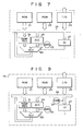
- Fig. 7 is a schematic of another embodiment of this invention in which the same numerals are used for the same parts in Fig. 2.
- the data generator 43 is connected between the accumulator 29 and the ALU 33.
- the encoding data which is preset by the data generator 43 is applied to the ALU 33 and the ROM data encryption is executed using this data.
- the encryption includes logical operations such as AND, OR and exclusive OR operations and arithmetic operation such as addition and subtraction. Such operations are executed by applying the fixed instruction code, which corresponds to the desired arithmetic or logical operation, to the instruction decoder 27 of microcomputer 19. This is executed by the particular hardware of the microcomputer in the same way as the regular program processing. Then, after processing has been executed on the data stored in the accumulator 29, the data is output through the I/O port 25.
- 8-bit data 1F, E7 and C4 in hexadecimal notation are stored, respectively at the addresses (N-l), (N) and (N+l) of ROM 21. Also, if these data 1F, E7 and C4 are exclusive ORed with the encrypting data 5A set in the data generator 43 at the ALU 33, the resulting data at the respective addresses will be 45, BD and 9E. Accordingly, it is impossible to recognize the contents of the ROM 21 from the output data.
- Fig. 9 shows another embodiment of this invention in which the code generator 37 shown in Fig. 2 is added to the embodiment shown in Fig. 7.
- the generated code from the code generator 37 is supplied to the instruction decoder 27 and the corresponding instruction is executed.
- ROM data encryption is performed using the encrypting data, and the result is output.
- Fig. 10 shows the embodiment of Fig. 9 as applied to the 8048 microcomputer.
- code generator 107 is provided between the bus 105 and the instruction decoder 104A and a data generator 108 is provided at the input of ALU 104D.
- the signals are applied to the external access terminal EA to read the contents of the mask ROM 101.
- the data read out from the ROM 101 is processed with the encrypting data from the data generator 108 and by the ALU function corresponding to the instruction code given by the code generator 107.
- This result is output on the data bus DBO through DB7.
- the code, from code generator 107 which is determined by the instruction set of the 8048, is output and supplied to the instruction decoder 104A for execution of a logic function.
- the encryption can be executed using the particular hardware of the 8048 in the same way as for a regular program.
- the only addition to the hardware that is required is the code generator 107 and data generator 108, which are simple to add.
- the data generator 43 may one that stores fixed data so the contents of data generator are set in the same manufacturing process as the contents of ROM 21. It is possible to use part of the ROM 21 as the data generator 43. It is also possible for the generator 43 to have the same values for all the data of ROM 21 or, to use different data for each constant address area of the ROM 21.
- the encryption is performed on the random data of the constant bit read out from the data generator 37 for each constant bit in the ROM 21, and the result is output.
- the instruction code and inherent hardware of the microcomputer 19 may be used to execute the encryption but special hardware may also be provided.
- Fig. 11 is a block diagram of this kind of microcomputer.
- a signal having a specified logic level is applied to a terminal (not shown) to output the contents of ROM 21 to the outside.
- the data read out from the ROM 21 is supplied to a second ALU 45 via a bus 35.
- Data is sent from data generator 43 to the second ALU 45 and operations, such as addition, subtraction and logic operations, are executed on it.
- the execution result is then output to the outside.
- the encrypting code of the code generator 107 or the encrypting data of the data generator 108 is set simultaneously with the mask ROM 101, which stores the predetermined program, it is not necessary to carry out a special process for the manufacture of the encrypting code or data. Also, it is possible to simply set different encrypting code or data for'all the contents of the mask ROM 101.
Abstract
Description
- This invention relates to a single-chip microcomputer which can read out the encrypted contents of a program memory.
- In recent years, program memory, data memory and input/output interface along with central processing unit have been integrated onto one chip. This chip, then, has come to be used as a single-chip microcomputer, or a computer on a chip.
- Fig. 1 is a block diagram showing an.example of such a
microcomputer 1. Thismicrocomputer 1 has amask ROM 3, which stores the programs, aRAM 5, which is used such as a temporary data storage and a work area and so on, an input/output port 7, an instruction decoder 9, which decodes the instructions of the program stored in theROM 3, anaccumulator 11, which is used to store intermediate calculation results and to perform arithmetic logic calculations, atemporary register 13 for temporarily storing the data on which an arithmetic logic unit operates, and an arithmetic logic unit 15 (ALU), which operates on the data stored in theaccumulator 11 andtemporary register 13. Each of these elements are connected through abus 17. The instructions read from theROM 3 are decoded by an instruction decoder 9 and, based on these control signals, the processing data is read from theRAM 5, or the input port, and set in thetemporary register 13 andaccumulator 11. The processed result by theALU 15 is stored in theRAM 5, or is transmitted to anoutput port 7 through thebus 17. - In order to verify the contents of the program memory, etc., this kind of microcomputer often is arranged so that the contents can be read out from the outside. An example of this kind of microcomputer is an 8-bit, single-chip microcomputer 8048 designed by Intel Corp. of the U.S.A. If the address is supplied to the Xl and X2 terminals (not shown) the address terminal and clock signals are supplied to and the timing signals are supplied to the EA and RESET terminals with specified timings, the contents at a designated address of the ROM will be output on the output terminals.
- In this kind of device, however, the program contents of the
ROM 3 can easily be read out by a third party, resulting in unexpected damage to the contents of this device, or the original maker of the application program on this device. In other words, a third party can read out the contents of the ROM and copy it. - There are microcomputers in which it is impossible to read out the contents of the ROM from the outside but these have the disadvantage that the program contents can not be verified in shipping and delivery inspections.
- Another method of preventing copying by a third party is to use a particular and exclusive code as the instruction code but this method results in reduced uses, difficulty in utilization of standard support softwares and difficulty in modifying the already developed programs.
- An object of the present invention is to provide a single-chip microcomputer with program contents that can be read out but cannot be copied by a third party.
- In order to achieve the above and other objects, there is provided according to the present invention a single-chip microcomputer with an encryptable program memory, comprising:
- a program memory which stores a program;
- a central processing unit which executes the program read out from said program memory;
- an input/output port which inputs and outputs to the outside data which is operated on by said central processing unit; and
- means for encrypting the contents of said program memory when the contents are output to the outside.
- Other objects and features of the present invention will be apparent from the following description which is given in conjunction with the accompanying drawings in which:
- Fig. 1 is a schematic of a prior art single-chip microcomputer;
- Fig. 2 is a block diagram showing an embodiment of the present invention;
- Fig. 3 shows an example of the data encryption in the embodiment of Fig. 2;
- Fig. 4 is a block diagram of another embodiment of the invention;
- Fig. 5 is a block diagram showing 8048 single-chip microcomputer of Intel Corp. U.S.A.;
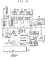
- Fig. 6 shows an example of this invention as applied to Intel's 8048 microcomputer;
- Fig. 7 is a block diagram showing another embodiment of this invention;
- Figs. 8A through 8C show an example of data encryption in the embodiment of Fig. 7;
- Fig. 9 is a block diagram showing another embodiment of this invention;
- Fig. 10 is a block diagram showing the embodiment of Fig. 9 as applied to the 8048 microcomputer; and
- Fig. 11 is a block diagram showing another embodiment of this invention.
- Now an embodiment of the present invention will be described referring to Fig. 2. In this embodiment, an arithmetic and logic unit (ALU) provided on the single-chip microcomputer is used to encrypt the data. The single-
chip microcomputer 19 of this invention with encryptable function of program memory includes amask ROM 21, which stores the programs, aRAM 23, which is used such as a temporary data storage and a work area, an input/output port 25, aninstruction decoder 27, which decodes the instructions of the program stored in theROM 21, anaccumulator 29, which is used to store intermediate computation results and to perform arithmetic logic operations, atemporary register 31 for temporarily storing the data on which an arithmetic and logic unit operates, and an arithmetic and logic unit(ALU) 33, which operates on the data stored in theaccumulator 29 andtemporary register 31. Each of these elements are connected by abus 35. The instructions read out from theROM 21 are decoded by aninstruction decoder 27 and, based on these control signals, the processing data is read out from theRAM 23 and I/O port, and set in thetemporary register 31 andaccumulator 29. The processed result by theALU 33 is stored in theRAM 23, or is output to the I/O port 25 through thebus 35. Thecode generator 37, which is the crux of this invention, is connected to theinstruction decoder 27. (This kind of a code generator may be a ROM structure.) - When a signal specifying the read out of the contents of
ROM 21 is supplied from the outside,code generator 37 sends a preset encrypting code to theinstruction decoder 27. Then, address, which corresponds to desired address of theROM 21, is input from the outside, and data corresonding to the address is read into theaccumulator 29, where the data is encrypted through a normal ALU function specified by the encryption code. - This data encryption or conversion instruction may be, for example, a shift instruction, a common instruction of microcomputers, which shifts the bit position of the data, a rotate instruction, which rotatingly shifts the bit position, or a complement instruction, which inverts the data in each bit position. When a shift or rotate instruction is executed, any shift direction or number of shift bit may be selected. With the complement instruction, the position of the bit to be inverted may be specified.
- In this way, the data read out from the
ROM 21 is encrypted and output on the I/O port 25. The result of which is that this output data is different from the memory contents of theROM 21. So, the copying by a third party is impossible and the data encryption function is unknown for a third party. - For example, as shown in Figs. 3A to 3C, 8-bit data which are 1F, E7 and C4 in hexadecimal are stored at addresses (N-l), (N) and (N+l), respectively. When data is output to the outside, if the data is rotated to the right by one bit, the values at addresses (N-l), (N) and (N+l) are converted to 8F, F3 and 62. Accordingly, the output data is entirely unrecognizable as the contents of the
ROM 21. - Accordingly, it is possible for the program stored in
ROM 21 to use the particular instruction code ofmicrocomputer 19 without any modification and, therefore, it is possible to use the standard support softwares and to easily improve the already developed application programs. - In other words, when the contents of the
ROM 21 are requested from the outside, the data is encrypted based on the output of thecode generator 37. Consequently, a third party, who of course is not familiar with the method of data encryption, will not be able to decode the contents and, accordingly, the actual program contents remain hidden. On the other hand, a user who does know the method of data decryption will be able to verify the read-out program and to reconstruct the program as it is before encryption so that the analyze of the read-out program can easily be performed. - One of the advantages of this invention is that the contents of
ROM 21 and the encryption code of thecode generator 37 can be set in the same manufacturing process so there is no increase in the number of processes for encrypting and it is possible to set the encryption code for individual data corresponding to the contents ofROM 21. - This invention is not limited to the above embodiment. In the above embodiment, the particular instruction code (hardware) of
microcomputer 19 is used to encrypt the data but, it is also possible for the encryption to be effected by hardware that is specifically for that purpose. This kind of special hardware may be provided in the input/output port, for example, when the data is read out of a special I/O port. This hardware would then operate only when the contents of the program memory are output. - Fig. 4 shows one example of this kind of microcomputer in which the data encryption is performed by a code encryptor provided in the output port.
- Fig. 5 is a block diagram of the widely used 8-bit Intel original microcomputer 8048. This
microcomputer 104 integrates a lK-byte mask ROM 101, a 64-byte RAM 102 and three groups of 8-bit I/O ports microprocessing unit 104, which has aninstruction decoder 104A,temporary register 104B,accumulator 104C and an arithmetic logic unit, onto one chip. All the elements are interconnected by aninternal bus 105. - When the contents of the
mask ROM 101, which is used as the program memory, are read out, +12V is applied to the EA external access terminal connected to the control andtiming circuit 106. By applying address to the lower 2-bit of the I/O port 103C and data bus DBO through DB7, the contents ofROM 101 which corresponds to this address are output through data bus DBO through DB7. - When this invention is applied to this kind of microcomputer, a code generator 107 may be provided between
bus 105 andinstruction decoder 104, for example. When the external signals for reading out the contents ofROM 101 is received, the indicated data is encrypted through the ALU function specified by the code from the code generator 107 and output on data bus DBO through DB7. Namely, a code, which is predetermined by the instruction code of the 8048, is output by code generator 107, and applied toinstruction decoder 104A for encryption. Accordingly, the encryption of the data is performed by using the particular hardware of the 8048 in the same way that a program is performed. The improvement to the hardware is only in relation to code generator 107 and is extremely easy. - Fig. 7 is a schematic of another embodiment of this invention in which the same numerals are used for the same parts in Fig. 2.
- In this embodiment, the
data generator 43 is connected between theaccumulator 29 and theALU 33. In this case, the encoding data, which is preset by thedata generator 43 is applied to theALU 33 and the ROM data encryption is executed using this data. The encryption includes logical operations such as AND, OR and exclusive OR operations and arithmetic operation such as addition and subtraction. Such operations are executed by applying the fixed instruction code, which corresponds to the desired arithmetic or logical operation, to theinstruction decoder 27 ofmicrocomputer 19. This is executed by the particular hardware of the microcomputer in the same way as the regular program processing. Then, after processing has been executed on the data stored in theaccumulator 29, the data is output through the I/O port 25. - For example, as is shown in Figs. 8A through 8C, 8-bit data 1F, E7 and C4 in hexadecimal notation are stored, respectively at the addresses (N-l), (N) and (N+l) of
ROM 21. Also, if these data 1F, E7 and C4 are exclusive ORed with the encrypting data 5A set in thedata generator 43 at theALU 33, the resulting data at the respective addresses will be 45, BD and 9E. Accordingly, it is impossible to recognize the contents of theROM 21 from the output data. - Fig. 9 shows another embodiment of this invention in which the
code generator 37 shown in Fig. 2 is added to the embodiment shown in Fig. 7. The generated code from thecode generator 37 is supplied to theinstruction decoder 27 and the corresponding instruction is executed. ROM data encryption is performed using the encrypting data, and the result is output. In this way, it is possible to make any logical processing using the particular hardware and instructions of themicrocomputer 19 in response to the encrypting code. Accordingly, when the contents of theROM 21 are read out to the outside, it is possible to execute different logical operations for each constant ROM area, for example, making it that much more difficult for a third party to decode the contents. - Of course, in this case as well, it is possible to set the contents of the
ROM 21,data generator 43 andcode generator 37 in the same manufacturing process so it is possible to set encrypting code for each of the contents ofROM 21. - Fig. 10 shows the embodiment of Fig. 9 as applied to the 8048 microcomputer. Namely, code generator 107 is provided between the
bus 105 and theinstruction decoder 104A and adata generator 108 is provided at the input ofALU 104D. The signals are applied to the external access terminal EA to read the contents of themask ROM 101. The data read out from theROM 101 is processed with the encrypting data from thedata generator 108 and by the ALU function corresponding to the instruction code given by the code generator 107. This result is output on the data bus DBO through DB7. In other words, the code, from code generator 107, which is determined by the instruction set of the 8048, is output and supplied to theinstruction decoder 104A for execution of a logic function. Accordingly, the encryption can be executed using the particular hardware of the 8048 in the same way as for a regular program. The only addition to the hardware that is required is the code generator 107 anddata generator 108, which are simple to add. - In the embodiments of Figs. 7 and 9, the
data generator 43 may one that stores fixed data so the contents of data generator are set in the same manufacturing process as the contents ofROM 21. It is possible to use part of theROM 21 as thedata generator 43. It is also possible for thegenerator 43 to have the same values for all the data ofROM 21 or, to use different data for each constant address area of theROM 21. When random data corresponding to all the contents of theROM 21 are stored in thedata generator 43 and a request of ROM readout is received, the encryption is performed on the random data of the constant bit read out from thedata generator 37 for each constant bit in theROM 21, and the result is output. - Also, in the above embodiment, the instruction code and inherent hardware of the
microcomputer 19 may be used to execute the encryption but special hardware may also be provided. - Fig. 11 is a block diagram of this kind of microcomputer. A signal having a specified logic level is applied to a terminal (not shown) to output the contents of
ROM 21 to the outside. The data read out from theROM 21 is supplied to asecond ALU 45 via abus 35. Data is sent fromdata generator 43 to thesecond ALU 45 and operations, such as addition, subtraction and logic operations, are executed on it. The execution result is then output to the outside. If the encrypting code of the code generator 107 or the encrypting data of thedata generator 108 is set simultaneously with themask ROM 101, which stores the predetermined program, it is not necessary to carry out a special process for the manufacture of the encrypting code or data. Also, it is possible to simply set different encrypting code or data for'all the contents of themask ROM 101.
Claims (15)
Applications Claiming Priority (4)
| Application Number | Priority Date | Filing Date | Title |
|---|---|---|---|
| JP191916/83 | 1983-10-14 | ||
| JP58191915A JPS6083157A (en) | 1983-10-14 | 1983-10-14 | One chip microcomputer |
| JP58191916A JPS6083158A (en) | 1983-10-14 | 1983-10-14 | One chip microcomputer |
| JP191915/83 | 1983-10-14 |
Publications (3)
| Publication Number | Publication Date |
|---|---|
| EP0137995A2 true EP0137995A2 (en) | 1985-04-24 |
| EP0137995A3 EP0137995A3 (en) | 1987-12-16 |
| EP0137995B1 EP0137995B1 (en) | 1990-10-17 |
Family
ID=26506985
Family Applications (1)
| Application Number | Title | Priority Date | Filing Date |
|---|---|---|---|
| EP84110235A Expired EP0137995B1 (en) | 1983-10-14 | 1984-08-28 | Single-chip microcomputer with encryptable function on program memory |
Country Status (3)
| Country | Link |
|---|---|
| US (1) | US4764959A (en) |
| EP (1) | EP0137995B1 (en) |
| DE (1) | DE3483410D1 (en) |
Cited By (4)
| Publication number | Priority date | Publication date | Assignee | Title |
|---|---|---|---|---|
| AT390148B (en) * | 1985-08-22 | 1990-03-26 | Novomatic Automatenindustrie U | ARRANGEMENT FOR DECRYLING COMMANDS |
| EP0449256A2 (en) * | 1990-03-27 | 1991-10-02 | Kabushiki Kaisha Toshiba | Microcontroller having security means |
| WO1996000953A2 (en) * | 1994-06-28 | 1996-01-11 | National Semiconductor Corporation | Secure data processor with cryptography and tamper detection |
| GB2308905A (en) * | 1996-01-08 | 1997-07-09 | John Robert Miller | Protected system processor |
Families Citing this family (25)
| Publication number | Priority date | Publication date | Assignee | Title |
|---|---|---|---|---|
| FR2601476B1 (en) * | 1986-07-11 | 1988-10-21 | Bull Cp8 | METHOD FOR AUTHENTICATING EXTERNAL AUTHORIZATION DATA BY A PORTABLE OBJECT SUCH AS A MEMORY CARD |
| US5146575A (en) * | 1986-11-05 | 1992-09-08 | International Business Machines Corp. | Implementing privilege on microprocessor systems for use in software asset protection |
| US5007082A (en) * | 1988-08-03 | 1991-04-09 | Kelly Services, Inc. | Computer software encryption apparatus |
| US5081675A (en) * | 1989-11-13 | 1992-01-14 | Kitti Kittirutsunetorn | System for protection of software in memory against unauthorized use |
| US5343524A (en) * | 1991-06-21 | 1994-08-30 | Mu Xiao Chun | Intelligent security device |
| JPH08305558A (en) * | 1995-04-27 | 1996-11-22 | Casio Comput Co Ltd | Ciphering program arithmetic unit |
| EP0852032A1 (en) * | 1995-07-20 | 1998-07-08 | Dallas Semiconductor Corporation | Single chip microprocessor, math co-processor, random number generator, real-time clock and ram having a one-wire interface |
| US5894515A (en) * | 1995-08-14 | 1999-04-13 | United Microelectronics Corporation | Random access memory device having inconsistent write-in and read-out data |
| US5937063A (en) * | 1996-09-30 | 1999-08-10 | Intel Corporation | Secure boot |
| US6014745A (en) * | 1997-07-17 | 2000-01-11 | Silicon Systems Design Ltd. | Protection for customer programs (EPROM) |
| KR100357177B1 (en) | 1998-01-13 | 2002-12-18 | 주식회사 하이닉스반도체 | Device for instruction interpretating of micro computer |
| US6320964B1 (en) | 1998-08-26 | 2001-11-20 | Intel Corporation | Cryptographic accelerator |
| US7421586B2 (en) * | 1999-05-12 | 2008-09-02 | Fraunhofer Gesselschaft | Protecting mobile code against malicious hosts |
| US6678833B1 (en) | 2000-06-30 | 2004-01-13 | Intel Corporation | Protection of boot block data and accurate reporting of boot block contents |
| JP3904432B2 (en) | 2001-11-16 | 2007-04-11 | 株式会社ルネサステクノロジ | Information processing device |
| KR100446317B1 (en) * | 2001-12-24 | 2004-09-01 | 주식회사 하이닉스반도체 | System for protecting data of code ROM in code ROM test |
| KR100474526B1 (en) * | 2002-07-19 | 2005-03-10 | 매그나칩 반도체 유한회사 | Control system with protective ability for external program code |
| US7877613B2 (en) * | 2002-09-04 | 2011-01-25 | Fraunhofer-Gesellschaft Zur Foerderung Der Angewandten Forschung E.V. | Protecting mobile code against malicious hosts |
| US20040064457A1 (en) * | 2002-09-27 | 2004-04-01 | Zimmer Vincent J. | Mechanism for providing both a secure and attested boot |
| RU2003131278A (en) * | 2002-10-29 | 2005-04-20 | Хай-О Информтех Эсдиэн Биэйчди (MY) | DATA ENCRYPTION METHOD |
| WO2005020514A1 (en) * | 2003-08-15 | 2005-03-03 | Thomson Licensing S.A. | Changeable functionality in a broadcast router |
| US20050141095A1 (en) * | 2003-12-29 | 2005-06-30 | Youngtack Shim | Reflecting sheet |
| KR20060127921A (en) | 2004-01-27 | 2006-12-13 | 코닌클리즈케 필립스 일렉트로닉스 엔.브이. | Protection against power analysis attacks |
| US20120210438A1 (en) * | 2011-02-15 | 2012-08-16 | Guobiao Zhang | Secure Three-Dimensional Mask-Programmed Read-Only Memory |
| US9514841B1 (en) | 2015-11-23 | 2016-12-06 | International Business Machines Corporation | Implementing eFuse visual security of stored data using EDRAM |
Citations (2)
| Publication number | Priority date | Publication date | Assignee | Title |
|---|---|---|---|---|
| US4278837A (en) * | 1977-10-31 | 1981-07-14 | Best Robert M | Crypto microprocessor for executing enciphered programs |
| EP0062438A2 (en) * | 1981-03-30 | 1982-10-13 | Fujitsu Limited | Microcomputer having memory content protecting means |
Family Cites Families (12)
| Publication number | Priority date | Publication date | Assignee | Title |
|---|---|---|---|---|
| US4168396A (en) * | 1977-10-31 | 1979-09-18 | Best Robert M | Microprocessor for executing enciphered programs |
| US4465901A (en) * | 1979-06-04 | 1984-08-14 | Best Robert M | Crypto microprocessor that executes enciphered programs |
| US4319079A (en) * | 1979-09-13 | 1982-03-09 | Best Robert M | Crypto microprocessor using block cipher |
| FR2469760A1 (en) * | 1979-11-09 | 1981-05-22 | Cii Honeywell Bull | METHOD AND SYSTEM FOR IDENTIFYING PEOPLE REQUESTING ACCESS TO CERTAIN MEDIA |
| US4543646A (en) * | 1980-06-05 | 1985-09-24 | Western Digital Corporation | Chip topography for MOS Data Encryption Standard circuit |
| US4433207A (en) * | 1981-09-10 | 1984-02-21 | Best Robert M | Cryptographic decoder for computer programs |
| US4471163A (en) * | 1981-10-05 | 1984-09-11 | Donald Thomas C | Software protection system |
| US4525599A (en) * | 1982-05-21 | 1985-06-25 | General Computer Corporation | Software protection methods and apparatus |
| US4555591A (en) * | 1982-09-07 | 1985-11-26 | At&T Bell Laboratories | Integrated circuit devices for secure data encryption |
| US4633388A (en) * | 1984-01-18 | 1986-12-30 | Siemens Corporate Research & Support, Inc. | On-chip microprocessor instruction decoder having hardware for selectively bypassing on-chip circuitry used to decipher encrypted instruction codes |
| US4598170A (en) * | 1984-05-17 | 1986-07-01 | Motorola, Inc. | Secure microprocessor |
| GB2163577B (en) * | 1984-08-23 | 1988-01-13 | Nat Res Dev | Software protection device |
-
1984
- 1984-08-28 DE DE8484110235T patent/DE3483410D1/en not_active Expired - Lifetime
- 1984-08-28 EP EP84110235A patent/EP0137995B1/en not_active Expired
- 1984-08-31 US US06/646,114 patent/US4764959A/en not_active Expired - Lifetime
Patent Citations (2)
| Publication number | Priority date | Publication date | Assignee | Title |
|---|---|---|---|---|
| US4278837A (en) * | 1977-10-31 | 1981-07-14 | Best Robert M | Crypto microprocessor for executing enciphered programs |
| EP0062438A2 (en) * | 1981-03-30 | 1982-10-13 | Fujitsu Limited | Microcomputer having memory content protecting means |
Non-Patent Citations (1)
| Title |
|---|
| ELECTRONICS, vol. 52, no. 13, 21st June 1979, pages 107-120, New York, US; H.J. HINDIN: "LSI-based data encryption discourages the data thief" * |
Cited By (7)
| Publication number | Priority date | Publication date | Assignee | Title |
|---|---|---|---|---|
| AT390148B (en) * | 1985-08-22 | 1990-03-26 | Novomatic Automatenindustrie U | ARRANGEMENT FOR DECRYLING COMMANDS |
| EP0449256A2 (en) * | 1990-03-27 | 1991-10-02 | Kabushiki Kaisha Toshiba | Microcontroller having security means |
| EP0449256A3 (en) * | 1990-03-27 | 1991-10-30 | Kabushiki Kaisha Toshiba | Microcontroller having security means |
| US5214697A (en) * | 1990-03-27 | 1993-05-25 | Kabushiki Kaisha Toshiba | Program execution apparatus for ensuring security of a program |
| WO1996000953A2 (en) * | 1994-06-28 | 1996-01-11 | National Semiconductor Corporation | Secure data processor with cryptography and tamper detection |
| WO1996000953A3 (en) * | 1994-06-28 | 1996-02-15 | Nat Semiconductor Corp | Secure data processor with cryptography and tamper detection |
| GB2308905A (en) * | 1996-01-08 | 1997-07-09 | John Robert Miller | Protected system processor |
Also Published As
| Publication number | Publication date |
|---|---|
| DE3483410D1 (en) | 1990-11-22 |
| US4764959A (en) | 1988-08-16 |
| EP0137995B1 (en) | 1990-10-17 |
| EP0137995A3 (en) | 1987-12-16 |
Similar Documents
| Publication | Publication Date | Title |
|---|---|---|
| EP0137995B1 (en) | Single-chip microcomputer with encryptable function on program memory | |
| US4633388A (en) | On-chip microprocessor instruction decoder having hardware for selectively bypassing on-chip circuitry used to decipher encrypted instruction codes | |
| US4593353A (en) | Software protection method and apparatus | |
| US11347898B2 (en) | Data protection device and method and storage controller | |
| US4905277A (en) | Method for enciphering and deciphering instructions in a microcomputer, and a microcomputer used for effecting same | |
| US6910094B1 (en) | Secure memory management unit which uses multiple cryptographic algorithms | |
| US5825878A (en) | Secure memory management unit for microprocessor | |
| KR100319677B1 (en) | Memory access control unit | |
| US4598170A (en) | Secure microprocessor | |
| US6286101B1 (en) | Central processing unit and microcomputer system having an internal operation unit for cryptographic | |
| JP2950571B2 (en) | Scrambler / Discrambler | |
| JP2000029790A (en) | Data security system | |
| JP2754786B2 (en) | Information processing device | |
| JP2000076144A (en) | Logic circuit, microcomputer and communication method between logic circuit and storage device | |
| JP2624249B2 (en) | Processor with imitation prevention function | |
| JPH0475137A (en) | Data processor | |
| JPH0223443A (en) | Microcomputer | |
| JPS59112341A (en) | Method for preventing leakage of secret information in software | |
| JPH03263147A (en) | Semiconductor integrated circuit device | |
| JPH02108141A (en) | Microcomputer | |
| JPH0547875B2 (en) | ||
| JPH01183735A (en) | Information processor | |
| JPS62233867A (en) | Read-only memory | |
| CN116756759A (en) | Method, chip and system for encrypting and decrypting algorithm of hybrid program | |
| JPH06139151A (en) | Microprocessor with security protection mechanism |
Legal Events
| Date | Code | Title | Description |
|---|---|---|---|
| PUAI | Public reference made under article 153(3) epc to a published international application that has entered the european phase |
Free format text: ORIGINAL CODE: 0009012 |
|
| 17P | Request for examination filed |
Effective date: 19840925 |
|
| AK | Designated contracting states |
Designated state(s): DE FR GB |
|
| PUAL | Search report despatched |
Free format text: ORIGINAL CODE: 0009013 |
|
| AK | Designated contracting states |
Kind code of ref document: A3 Designated state(s): DE FR GB |
|
| 17Q | First examination report despatched |
Effective date: 19890907 |
|
| GRAA | (expected) grant |
Free format text: ORIGINAL CODE: 0009210 |
|
| AK | Designated contracting states |
Kind code of ref document: B1 Designated state(s): DE FR GB |
|
| REF | Corresponds to: |
Ref document number: 3483410 Country of ref document: DE Date of ref document: 19901122 |
|
| ET | Fr: translation filed | ||
| PLBE | No opposition filed within time limit |
Free format text: ORIGINAL CODE: 0009261 |
|
| STAA | Information on the status of an ep patent application or granted ep patent |
Free format text: STATUS: NO OPPOSITION FILED WITHIN TIME LIMIT |
|
| 26N | No opposition filed | ||
| REG | Reference to a national code |
Ref country code: GB Ref legal event code: 746 Effective date: 19981026 |
|
| REG | Reference to a national code |
Ref country code: FR Ref legal event code: D6 |
|
| PGFP | Annual fee paid to national office [announced via postgrant information from national office to epo] |
Ref country code: FR Payment date: 20010810 Year of fee payment: 18 |
|
| PGFP | Annual fee paid to national office [announced via postgrant information from national office to epo] |
Ref country code: DE Payment date: 20010820 Year of fee payment: 18 |
|
| PGFP | Annual fee paid to national office [announced via postgrant information from national office to epo] |
Ref country code: GB Payment date: 20010822 Year of fee payment: 18 |
|
| REG | Reference to a national code |
Ref country code: GB Ref legal event code: IF02 |
|
| PG25 | Lapsed in a contracting state [announced via postgrant information from national office to epo] |
Ref country code: GB Free format text: LAPSE BECAUSE OF NON-PAYMENT OF DUE FEES Effective date: 20020828 |
|
| PG25 | Lapsed in a contracting state [announced via postgrant information from national office to epo] |
Ref country code: DE Free format text: LAPSE BECAUSE OF NON-PAYMENT OF DUE FEES Effective date: 20030301 |
|
| GBPC | Gb: european patent ceased through non-payment of renewal fee |
Effective date: 20020828 |
|
| PG25 | Lapsed in a contracting state [announced via postgrant information from national office to epo] |
Ref country code: FR Free format text: LAPSE BECAUSE OF NON-PAYMENT OF DUE FEES Effective date: 20030430 |
|
| REG | Reference to a national code |
Ref country code: FR Ref legal event code: ST |