EP0040838A1 - Detector and analysing system for fingerprints - Google Patents
Detector and analysing system for fingerprints Download PDFInfo
- Publication number
- EP0040838A1 EP0040838A1 EP81103955A EP81103955A EP0040838A1 EP 0040838 A1 EP0040838 A1 EP 0040838A1 EP 81103955 A EP81103955 A EP 81103955A EP 81103955 A EP81103955 A EP 81103955A EP 0040838 A1 EP0040838 A1 EP 0040838A1
- Authority
- EP
- European Patent Office
- Prior art keywords
- scanning
- fingerprint
- scanning surface
- finger
- temperature
- Prior art date
- Legal status (The legal status is an assumption and is not a legal conclusion. Google has not performed a legal analysis and makes no representation as to the accuracy of the status listed.)
- Withdrawn
Links
Images


Classifications
-
- A—HUMAN NECESSITIES
- A61—MEDICAL OR VETERINARY SCIENCE; HYGIENE
- A61B—DIAGNOSIS; SURGERY; IDENTIFICATION
- A61B5/00—Measuring for diagnostic purposes; Identification of persons
- A61B5/117—Identification of persons
- A61B5/1171—Identification of persons based on the shapes or appearances of their bodies or parts thereof
- A61B5/1172—Identification of persons based on the shapes or appearances of their bodies or parts thereof using fingerprinting
-
- G—PHYSICS
- G06—COMPUTING; CALCULATING OR COUNTING
- G06V—IMAGE OR VIDEO RECOGNITION OR UNDERSTANDING
- G06V40/00—Recognition of biometric, human-related or animal-related patterns in image or video data
- G06V40/10—Human or animal bodies, e.g. vehicle occupants or pedestrians; Body parts, e.g. hands
- G06V40/12—Fingerprints or palmprints
- G06V40/13—Sensors therefor
Definitions
- the present invention relates to a fingerprint converter according to the preamble of claim 1 and to a method for analyzing a fingerprint.
- the finger to be checked is usually pressed against a flat surface, for example on one side of a glass plate, and the pattern of the finger consisting of ridges and furrows is scanned by scanning devices, for example an interrogating light beam.
- the processing of the fingerprint information thus obtained can include laser techniques.
- Such devices for identifying fingerprints are generally used to control the access of individuals to information (information access control), for example to computer terminals (information access control) or to buildings (physical access control).
- weak fingerprints are fingerprints that have a low modulation depth on the scanning surface or, in other words, a low topographical relief value.
- a weak fingerprint can occur if the finger to be tested is not pressed hard against the scanning surface, if the finger does not have enough liquid, for example oil or moisture, and is therefore insufficient - Ed 1 Sti / 25.3.81
- a fingerprint input sensor or transducer is therefore required which is designed in such a way that it can scan not only fingerprints of regular quality, but also weak fingerprints with a low modulation depth. There is also a need for a method for easily analyzing fingerprints.
- the fingerprint converter should enable the information contained in the structure of a human fingerprint to be transferred to a terminal for verification, so that a maximum amount of information contained in the skin structure can be obtained.
- the fingerprint converter should work quickly and be reusable after every analysis or verification attempt.
- US Pat. No. 4,053,228 discloses a finger identification problem in which a fingerprint is created by pressing a finger against the back surface of a transparent glass plate and holding the finger thereon in a predetermined position. This fingerprint is scanned or queried by a light beam that is radiated through the front surface of the glass plate. The interrogating beam is partially reflected on the rear surface of the glass plate, thereby generating a signal beam which carries fingerprint information.
- the back surface of the glass plate is covered with a coating, which serves to increase the difference in reflectivity between the furrows and ribs of the fingerprint.
- the coating on the back surface reinforces the difference between the reflectivity on that surface between those fields in which the ribs of the finger are in intimate contact with the back surface of the plate and those fields under the furrows of the finger in which air with the rear surface of the Plate is in contact.
- a reinforced fingerprint is only generated as long as the finger touches the back surface of the plate and this is brief.
- U.S. Patent 4,120,585 discloses a resilient elastic prism for use in an optical imaging system, e.g. a fingerprint reader.
- the base of the prism is touched by the finger to be examined.
- the compliant prism deforms under the pressure of the touching finger.
- Light from a light source shines through one side surface of the prism towards the base surface, where it reflects and shines through the other side surface towards a light-sensitive element.
- This element is intended for triggering or actuating the optical imaging system. If there is sufficient fingerprint, an air gap is created between the base surface and a housing, which results in an additional field, the light beam of which is directed towards the photosensitive element. This element activates the system by closing a switch.
- This fingerprint system does not discuss facilities for processing weak fingerprints.
- the captured charges form an electrostatic surface charge layer in which the charge density distribution is directly proportional to the exposure distribution of the input signal.
- the resulting electrical field distribution causes a deformation of the elastomer, whereby a surface relief pattern is generated which is directly related to the exposure distribution due to the surface charge density. The deformation continues until the uneven charge distribution is maintained.
- this memory device has not been considered for use as a fingerprint converter.
- thermoplastic data storage medium has become known from SPIE, Vol. 123, Optical Storage Materials and Methods (1977) pp. 32-36.
- This medium is a multilayer device which consists of a thermoplastic layer, a photoconductive layer and a transparent conductive layer on a glass substrate or flexible polyester substrate.
- Optical data storage in thermoplastics is based on the principle that a thermoplastic deforms under pressure when heated to a suitable temperature. During the writing process, a uniform charge is generated on the thermoplastic surface, then the device is exposed with a holographic pattern, which changes the conductivity of the photoconductor and consequently the surface charge distribution. The device is then exposed to an optical pattern which changes the conductivity of the photoconductor and consequently the surface charge distribution.
- This uneven charge distribution results in electrostatic forces, which deform the thermoplastic when heated to a critical softening or development temperature.
- the deformation corresponding to the optical pattern is retained and the information can be reproduced by illumination with a readout beam.
- This storage medium is also not intended for use as a fingerprint converter.
- the invention is based on the object of specifying a fingerprint input sensor or transducer of simple construction which is able to determine and sense a considerable amount of information contained in the main structure of a human fingerprint or to specify a method for analyzing a fingerprint on a surface.
- the fingerprint converter according to the invention or the method according to the invention works quickly, can be used again after a previous fingerprint examination, a fingerprint can be stored for a certain period of time and a fingerprint can be optically read out in transmission or reflection.
- the fingerprint input transducer comprises a scanning element which has a scanning surface for receiving a fingerprint.
- the scanning surface has a surface relief with a random spatial frequency distribution.
- These elevations, elements or points are preferably made of the same material as the scanning element. They are small compared to the fingerprint. Their size is chosen so that considerable light scattering can be observed when the surface is illuminated.
- the sensing element is made of a material that has a transition or softening temperature that is higher than the ambient temperature and is close to the temperature of the finger or human body.
- the softening temperature is selected so that the material of the element begins to melt when the finger is pressed on the scanning surface. This melting process arises due to the pressure and / or heat exerted on the surface by the finger.
- the softening temperature of the sensing element should be about 40 ° C or higher.
- the softening temperature is preferably only a few degrees Celsius above the temperature of the human body.
- the scanning element can be made of an elastic or soft material. It is preferably made of an elastomeric or thermoplastic material, for example of plasticized polystyrene. It can also be made of a material whose properties are similar to those of an elastomeric material.
- An elastomeric material is to be understood to mean any one of those different polymers which have the elastic properties of natural rubber. In particular, an elastomer with a comparatively low softening temperature can be selected.
- Thermoplastics are polymers that can be repeatedly softened (melted) by heat and hardened by cooling. Typical thermoplastics are polyethylene, polypropylene, polystyrenes, polyacrylics, polyvenyls, nylon fabrics and fluoropolymers.
- a device for generating an electrostatic charge on the scanning surface can be provided, as well as a heating device for heating the scanning surface on the scanning element to a temperature which at least corresponds to the softening temperature of the material, from which the scanning element is made.
- the charge mentioned above can be generated on the surface, preferably by a corona charge.
- the charging device can Contain wire, which is arranged at a distance from the surface of the scanning element, and a voltage source for applying a DC voltage between the wire and the surface of the scanning element.
- the charging device can also comprise a flat electrode in the form of a wire grid, which is arranged close to the surface of the scanning element, and a voltage source for applying a direct voltage between the electrode and the scanning element.
- the above-mentioned heater can be an electric heater. It can contain a heating resistor, which can be, for example, a resistance wire, a flat wire grid or a transparent electrode that has a suitable sheet resistance. A heating current flows through the heating resistor during operation.
- the wire mesh can be transparent with respect to the wavelength of the scanning light beam. To achieve good heat coupling, the heating resistor can be attached to the sensing element.
- the heating device need not necessarily be an ohmic heating device or resistance heating.
- the heating can also be achieved by radiation.
- heat can be transferred to the scanning surface by means of an infrared (IR) laser, in particular an IR LED, by means of a semiconductor laser or by means of similar IR light sources.
- IR infrared
- the fingerprint information stored in the scanning element can be read out either by optical devices, for example in total reflection, or by laser optics in a known manner.
- the topographical relief can be analyzed in any known manner.
- a surface relief of random spatial frequency distribution and random orientation is generated on a scanning surface of a scanning element in a first step.
- the finger to be examined is pressed against the surface of the scanning element, so that it leaves a surface relief. Due to the temperature and pressure of the finger, the random surface relief melts locally, preferably at locations where the ribs or elevations of the finger touch the scanning element. At these points, the random distribution of the surveys is destroyed. The consequence of this is that the molten parts no longer scatter light in the same way as the undamaged environment. This means that the transducer can easily read the fingerprint using optical means.
- the scanning surface is heated and at the same time electrostatically charged. Then the surface is cooled below the softening temperature. For example, a heating current can be passed through the heating resistor thermally coupled to the elastomeric material. When the scanning surface is heated, it becomes soft and the melted surface becomes flatter due to the surface tension. However, a random relief is created because of the loading. The transducer is thus prepared for a new fingerprint identification cycle.
- One of the advantages of the present invention is that the enhanced relief on the surface of the sensing element remains stable or "frozen” after the finger is pressed against the sensing surface.
- a rectangular flat plate is provided as the scanning element 2.
- the scanning element 2 has a first surface, called the scanning surface 3, and a second surface, called the lower surface 4.
- the scanning element 2 is made of material which is reusable, preferably of an elastomeric or thermoplastic material, for example plasticized polystyrene.
- the material of the scanning element 2 is not electrically conductive. It is selected so that its transition or softening temperature is higher than the ambient temperature surrounding the element and close to the temperature of the human body. In particular, the softening temperature should be selected so that it is greater than about 40 ° C. It can be chosen so that it is only a few degrees Celsius above the ambient temperature.
- the scanning surface 3 is designed such that it receives the pressure of a finger 5 to be examined shown in FIG. 3 for a short period of time.
- the softening temperature is selected so that a thin layer of the material of the scanning surface 3 begins to melt when the finger 5 is pressed onto it.
- the scanning surface 3 of the scanning element 2 need not be flat. It can also be curved in such a way that it is adapted to the outline of the finger 5.
- the electrode 6 is attached to the second surface 4.
- the electrode 6 is preferably made of a material which is transparent with regard to the light of an interrogating beam, which is indicated in FIGS. 5 and 6. It can be made of indium oxide (In0).
- the electrode 6 is in the form of a thin rectangular plate or a corresponding wire system, or can be in the form of a thin film coating.
- the electrode 6 can be grounded. It is translucent Carrier plate 7 worn, for example by a glass substrate.
- the scanning surface 3 has a surface relief of a random configuration.
- the surface 3 contains many small elevations and / or depressions in a random distribution. These variations in the elevations in or on the surface, which have no special pattern, can preferably be generated in a manner described in more detail below.
- all segments Upon exposure of area 3, all segments would scatter the light in a random manner so that there was no preferred direction of scattering.
- the creation of a thin surface relief of random configuration forms a first process step.
- a second method step the finger 5 is pressed against the flat scanning surface 3 of the scanning element 2. This can be seen in FIG. 3.
- the next step in the method is to remove the finger 5 from the scanning surface 3. As shown in FIG. 4, a fingerprint 8 has been left on the surface 3. Due to the pressure or temperature exerted on the surface 3 by the elevations of the finger, the random surface relief melts locally. There are no elevations or depressions in the melted sections. These sections are "ironed out"; they now form flat areas.
- FIG. 5 Areas or sections in which a statistical distribution is still present are designated by 8a and areas or sections in which the statistical distribution of the small depressions and / or elevations have been “ironed out” by the elevations of the finger are designated by 8b.
- FIGS. 5 and 6 The next process step is shown in FIGS. 5 and 6.
- the information contained in the "frozen" fingerprint is optically read out and analyzed.
- This can be carried out by means of the light of an interrogating or reading beam 9 either in transmission or in reflection.
- the embodiment according to FIGS. 5 and 6 shows reading out by means of transmitting light.
- the beam 9 is directed perpendicularly onto the lower surface 4 of the scanning element 2. For this' end of the beam 9 is transmitted through the transparent member 7 and the transparent electrode 6 in the sensing element. 2 Finally, it reaches the upper surface 3. After it has passed the fingerprint 8, it carries the fingerprint information.
- the light is spatially modulated in accordance with the depressions and elevations of the surface 3, ie it carries the information about the geometric structure of the fingerprint 8.
- the analysis of the information contained in the modulated light can in principle be carried out in any known manner. However, a very simple method is illustrated in FIGS. 5 and 6.
- the light is scattered only in narrow cones 10a which surround the optical axis of the illuminating beam (forward scattering).
- the illuminating beam is scattered in wide-open cones 10a. This means that the molten parts of element 2 no longer scatter light in the same way as in the undamaged environment.
- the fingerprint pattern can be seen in the form of dark lines on an illuminated background if the surface 3 is seen at an acute angle ⁇ relative to the normal.
- the picture the scanning surface 3 and the image 8 ′ of the fingerprint 8 can be directed onto a light-sensitive device 12 via an optical system 11.
- This device 12 can consist of a field of photo electrodes for converting the image into electrical signals.
- the fingerprint sensor is reset to its original state.
- This step involves electrostatic charging and simultaneous heating.
- a device for electrostatic charging and a heating device are provided for this purpose.
- the device for charging comprises a voltage source 14 with a high voltage V, which can be switched between ground and an electrode 15 by means of a switch 16.
- the electrode 15 is arranged at a distance from the scanning surface 3. It is carried by a carrier element 17, for example by a glass substrate.
- the electrode 15 can consist of a single wire which is arranged parallel to the surface 3. In the present embodiment, it consists of a flat electrode, which is connected to the lower surface of the carrier element 1'7.
- the high voltage V between the electrodes 6 and 15 causes the air in the vicinity of the electrode 15 to be ionized. Due to the ionization of the air, electrical charges are directed to the scanning surface 3. These charges are kept on surface 3. They cannot flow away from the surface 3 because the scanning element 2 forms an electrical insulator.
- the positive connection of the high voltage source 14 is connected to the electrode 15, while the negative connection is connected to the electrode 6. Therefore surface 3 is charged with positive particles. However, charging with negative particles is also possible. To obtain a negative electrostatic charge, it is only necessary to reverse the polarity of the high voltage source 14 with respect to the electrodes 6 and 15. As indicated in FIG. 7, the positive particles would collect in certain surface elements in the area of the fingerprint 8 without heating. Due to the locally varying charge density, different electrical field strengths would be present and different electrical forces would be exerted on different surface elements.
- FIG. 7 also shows a heating device which, in the present embodiment, is electrical in nature, in particular consists of a resistance heating device.
- the heating device consists of a heating current source 18 and a switch 19.
- the heating current source 18 and the switch 19 are connected in series between one end of the electrode 6 and ground. The other end of the electrode 6 is also connected to ground.
- the heating current source 18 supplies a heating current (direct current or pulsating current) which flows through the electrode 6.
- the electrode 6 is not only a high-voltage electrode that is used for electrostatic charging, it is also a heating resistor, for example a resistance grid.
- the heating current heats the sensing element 2.
- the size of the heating current is selected so that a temperature is reached on the scanning surface 3 which corresponds at least approximately to the softening temperature of the elastomeric or thermoplastic material.
- the surface 3 of the scanning element 2 becomes soft and begins to melt. Now the surface 3 can become flat or smooth and the fingerprint 8 is erased.
- the electrostatic charge spreads randomly on the surface, whereby electrostatic forces are exerted on the surface 3 that result in a random distribution of depressions and / or surveys. The result of this is that a transducer is obtained again which has statistical surface properties. This effect is known in the literature as the frost effect of thermoplastic media.
- the last process step is to cool the scanning element 2. This can be achieved simply by switching off the switch 19, provided that the ambient temperature is low enough.
- a cooling device not shown, can be connected to the scanning element 2, for example thermoelectric Peltier elements. The cooling of the scanning element 2 results in a "freezing" of the random pattern relief of the surface 3. It should be noted that the electrode 15 is switched off from the high voltage source 14 during the cooling process. After cooling, the scanning element 2 is for the next fingerprinting process and reading cycle. ready.
- the heating of the scanning element 2 can also be achieved by means of a radiant heating device.
- an IR radiation source 20 is used, which emits IR radiation 21 in the direction of the lower side of the electrode 6.
- the IR source 20 can be a single IR source or an array of individual IR sources.
- An IR radiation-imitating LED or an IR lamp can be used as the IR source 20.
- FIG. 11 shows a perspective illustration of another embodiment of the invention.
- the electrode 15 for charging the upper surface of the element consists of a field of parallel wires which are connected on one side to a connecting element 23, which in turn is connected to the high voltage source 14 via the switch 1'6.
- the array of parallel wires can be held by suitable devices, which are not shown.
- FIG. 12 shows a perspective illustration of yet another embodiment of the invention.
- the electrode 15 consists of a single wire, which is held parallel to the surface of the element 2 '.
- the electrode 15 is shielded by a screen 25 on the side facing away from the surface 3. Therefore, charged particles are generated substantially between the screen 25 and the upper surface 3 of the sensing element 2.
Abstract
Es wird ein Fingerabdruckwandler beschrieben, der ein Abtastelement (2) umfaßt, das eine Abtastfläche (3) zur Aufnahme eines Fingerabdrucks (8) aufweist. Das Abtastelement (2) ist aus einem Material gefertigt, welches eine Übergangs- oder Erweichungstemperatur aufweist die höher als die Umgebungstemperatur und in der Nähe der Temperatur des Fingers liegt. Die Erweichungstemperatur ist insbesondere so gewählt, daß das Material des Abtastelements (2) an der Oberfläche zu schmelzen beginnt, wenn der Finger auf die Abtastfläche (3) gedrückt wird. Die Abtastfläche (3) weist ein Oberflächenrelief zufälliger räumlicher Verteilung auf. Anders ausgedrückt: die Abtastfläche (3) weist verschiedene Erhebungen auf, die kein spezielles Muster zeigen. Es wird auch ein Verfahren zur Analysierung von Fingerabdrücken beschrieben, welches folgende Verfahrensschritte aufweist: Auf einer Abtastfläche (3) eines Abtastelements (2) wird ein Oberflächenrelief mit zufälliger räumlicher Verteilung erzeugt. Auf der Abtastfläche (3) wird durch Aufdrücken eines Fingers ein Fingerabdruck erzeugt. Der Fingerabdruck wird aus der Abtastfläche (3) optisch ausgelesen.A fingerprint transducer is described which comprises a scanning element (2) which has a scanning surface (3) for receiving a fingerprint (8). The scanning element (2) is made of a material which has a transition or softening temperature which is higher than the ambient temperature and close to the temperature of the finger. The softening temperature is chosen in particular so that the material of the scanning element (2) begins to melt on the surface when the finger is pressed onto the scanning surface (3). The scanning surface (3) has a surface relief of random spatial distribution. In other words: the scanning surface (3) has different elevations that do not show a special pattern. A method for analyzing fingerprints is also described, which has the following method steps: A surface relief with a random spatial distribution is generated on a scanning surface (3) of a scanning element (2). A fingerprint is generated on the scanning surface (3) by pressing on a finger. The fingerprint is read optically from the scanning surface (3).
Description
Die vorliegende.Erfindung bezieht sich auf einen Fingerabdruckwandler nach dem Oberbegriff des Patentanspruchs 1 und auf ein Verfahren zum Analysieren eines Fingerabdrucks.The present invention relates to a fingerprint converter according to the preamble of claim 1 and to a method for analyzing a fingerprint.
In einem Fingerabdruck-Eingabewandler oder -sensor wird der zu überprüfende Finger gewöhnlich gegen eine flache Oberfläche gedrückt, beispielsweise auf eine Seite einer Glasplatte und das aus Rippen und Furchen bestehende Muster des Fingers wird durch Abtasteinrichtungen, beispielsweise einen abfragenden Lichtstrahl abgetastet. Die Verarbeitung der auf diese Weise erhaltenen Fingerabdruckinformation kann Lasertechniken umfassen. Derartige Vorrichtungen zur Identifizierung von Fingerabdrücken werden im allgemeinen zur Kontrolle des Zugangs von Individuen zu Informationen (Informationszugangskontrolle), beispielsweise zu Rechnerendgeräten (Informationszugangskontrolle) oder zu Gebäuden (physische Zugriffskontrolle) benutzt.In a fingerprint input transducer or sensor, the finger to be checked is usually pressed against a flat surface, for example on one side of a glass plate, and the pattern of the finger consisting of ridges and furrows is scanned by scanning devices, for example an interrogating light beam. The processing of the fingerprint information thus obtained can include laser techniques. Such devices for identifying fingerprints are generally used to control the access of individuals to information (information access control), for example to computer terminals (information access control) or to buildings (physical access control).
Eines der im Zusammenhang mit Fingerabdrucksensoren stehenden Probleme betrifft die zuverlässige Abtastung schwacher Fingerabdrücke. "Schwache Fingerabdrücke" sind Fingerabdrücke, die eine geringe Modulationstiefe auf der Abtastfläche aufweisen oder anders ausgedrückt, einen geringen topografischen Reliefwert. Ein schwacher Fingerabdruck kann auftreten, wenn der zu prüfende Finger nicht stark gegen die Abtastfläche gedrückt wird, wenn der Finger nicht genügend Flüssigkeit, beispielsweise Öl oder Feuchtigkeit, aufweist und dadurch keine ausreichen-Ed 1 Sti/25.3.81One of the problems associated with fingerprint sensors concerns the reliable scanning of weak fingerprints. "Weak fingerprints" are fingerprints that have a low modulation depth on the scanning surface or, in other words, a low topographical relief value. A weak fingerprint can occur if the finger to be tested is not pressed hard against the scanning surface, if the finger does not have enough liquid, for example oil or moisture, and is therefore insufficient - Ed 1 Sti / 25.3.81
den:Spuren auf der Fläche hinterläßt, usw.. Es wird deshalb ein Fingerabdruck-Eingabesensor oder -wandler benötigt, der so ausgebildet ist, daß er nicht nur Fingerabdrücke regulärer Qualität, sondern auch schwache Fingerabdrücke geringer Modulationstiefe abtasten kann. Es besteht auch ein Bedarf für ein Verfahren zur leichten Analysierung von Fingerabdrücken.: Leaves traces on the surface, etc. A fingerprint input sensor or transducer is therefore required which is designed in such a way that it can scan not only fingerprints of regular quality, but also weak fingerprints with a low modulation depth. There is also a need for a method for easily analyzing fingerprints.
Allgemein gesprochen sollte der Fingerabdruckwandler die Übertragung der in der Struktur eines menschlichen Fingerabdrucks enthaltenen Information in ein Endgerät zur Verifikation ermöglichen, so daß ein maximaler in der Hautstruktur enthaltener Informationsbetrag erlangt werden kann. Der Fingerabdruckwandler sollte schnell arbeiten und nach jedem Analysierungs- oder Verifikationsversuch wiederbenutzbar sein.Generally speaking, the fingerprint converter should enable the information contained in the structure of a human fingerprint to be transferred to a terminal for verification, so that a maximum amount of information contained in the skin structure can be obtained. The fingerprint converter should work quickly and be reusable after every analysis or verification attempt.
Aus der US-PS 4 053 228 geht ein Fingeridentifizierungsproblem hervor, in welchem ein Fingerabdruck dadurch erzeugt wird, daß ein Finger gegen die Rückfläche einer transparenten Glasplatte gedrückt und der Finger in einer vorbestimmten Lage darauf gehalten wird. Dieser Fingerabdruck wird von einem, durch die Vorderfläche der Glasplatte gestrahlten Lichtstrahl abgetastet oder abgefragt. Der abfragende Strahl wird teilweise an der Rückfläche der Glasplatte reflektiert und dadurch ein Signalstrahl erzeugt, welcher Fingerabdruckinformation trägt. Die Rückfläche der Glasplatte ist mit einem Überzug überdeckt, welcher dazu dient, den Unterschied im Reflexionsvermögen zwischen den Furchen und Rippen des Fingerabdrucks zu verstärken. Insbesondere verstärkt der Überzug auf der Rückfläche den Unterschied zwischen dem Reflexionsvermögen auf dieser Fläche zwischen jenen Feldern, in denen die Rippen des Fingers in innigem Kontakt mit der Rückfläche der Platte stehen und jenen Feldern unter den Furchen des Fingers, in denen Luft mit der Rückfläche der Platte in Kontakt steht. In diesem Fingerabdruckwandler wird ein verstärkter Fingerabdruck nur so lange erzeugt, wie der Finger die Rückfläche der Platte berührt und dies ist kurzzeitig.US Pat. No. 4,053,228 discloses a finger identification problem in which a fingerprint is created by pressing a finger against the back surface of a transparent glass plate and holding the finger thereon in a predetermined position. This fingerprint is scanned or queried by a light beam that is radiated through the front surface of the glass plate. The interrogating beam is partially reflected on the rear surface of the glass plate, thereby generating a signal beam which carries fingerprint information. The back surface of the glass plate is covered with a coating, which serves to increase the difference in reflectivity between the furrows and ribs of the fingerprint. In particular, the coating on the back surface reinforces the difference between the reflectivity on that surface between those fields in which the ribs of the finger are in intimate contact with the back surface of the plate and those fields under the furrows of the finger in which air with the rear surface of the Plate is in contact. In this Fingerprint converter, a reinforced fingerprint is only generated as long as the finger touches the back surface of the plate and this is brief.
Aus der US-PS 4 120 585 ist ein nachgiebiges elastisches Prisma zum Gebrauch in einem optischen Abbildungssystem z.B. einem Fingerabdruckleser, bekannt geworden. Die Basisfläche des Prismas wird von dem zu untersuchenden Finger berührt. Das nachgiebige Prisma verformt sich unter dem Druck des berührenden Fingers. Licht aus einer Lichtquelle durchstrahlt eine Seitenfläche des Prismas in Richtung Basisfläche, wo es reflektiert und durch die andere Seitenfläche in Richtung eines lichtempfindlichen Elements strahlt. Dieses Element ist zum Auslösen oder Betätigen des optischen Abbildungssystems vorgesehen. Wenn ausreichender Fingerabdruck vorhanden ist, wird zwischen der Basisfläche und einem Gehäuse ein Luftspalt erzeugt, der in einem zusätzlichen Feld resultiert, dessen Lichtstrahl zum lichtempfindlichen Element gerichtet wird. Dieses Element aktiviert das System, in dem es einen Schalter schließt. Bei diesem Fingerabdrucksystem werden keine Einrichtungen zum Verarbeiten schwacher Fingerabdrücke erörtert.U.S. Patent 4,120,585 discloses a resilient elastic prism for use in an optical imaging system, e.g. a fingerprint reader. The base of the prism is touched by the finger to be examined. The compliant prism deforms under the pressure of the touching finger. Light from a light source shines through one side surface of the prism towards the base surface, where it reflects and shines through the other side surface towards a light-sensitive element. This element is intended for triggering or actuating the optical imaging system. If there is sufficient fingerprint, an air gap is created between the base surface and a housing, which results in an additional field, the light beam of which is directed towards the photosensitive element. This element activates the system by closing a switch. This fingerprint system does not discuss facilities for processing weak fingerprints.
Aus STIE, Vol. 185, Optical Processing Systems (1979) S. 86 - 92 ist eine elastomere Speichervorrichtung bekannt geworden, die einen Fotoleiter benutzt. Ein Glassubstrat wird zur Bildung einer transparenten leitenden Grundebene chemisch geätzt. Die Grundebene wird mit dem erwähnten Fotoleiter bedeckt und mit einer dünnen elastomeren Schicht überzogen.From STIE, Vol. 185, Optical Processing Systems (1979) pp. 86-92, an elastomeric storage device using a photoconductor has become known. A glass substrate is chemically etched to form a transparent conductive base layer. The base plane is covered with the aforementioned photoconductor and covered with a thin elastomer layer.
Mehrere 10/um (mehrere mils) über der elastomeren Oberfläche und parallel dazu ist eine Ladungsfläche, insbesondere-ebene angeordnet. Der daraus resultierende Spalt ist mit Argon unter niedrigem Druck gefüllt. Während des Betriebes ist zwischen der Ladungsfläche und der Grundfläche eine Hochspannungsquelle geschaltet, die eine quer zu der elastomerischen oder fotoleitenden Schicht gerichtete elektrostatische Kraft erzeugt. Die elektrostatische Kraft steht senkrecht auf der elastomerischen Oberfläche und ist in jedem Punkt der elektrischen Feldstärke proportional. Weil das Elastomer inkompressibel und die Kraft gleichmäßig ist, tritt keine Verformung auf. Wenn der Fotoleiter einer Lichtverteilung ausgesetzt wird, werden Ladungsträgerfotos erzeugt und bewegen sich in dem elektrischen Feld in Richtung zur Grenzfläche zwischen Elastomer und Fotoleiter, wo sie aufgefangen werden. Die aufgefangenen Ladungen bilden eine elektrostatische Oberflächenladungsschicht, in welcher die Ladungsdichteverteilung direkt proportional zur Belichtungsverteilung des Eingangssignals ist. Die resultierende elektrische Feldverteilung bewirkt eine Verformung des Elastomers, wobei ein Oberflächenreliefmuster erzeugt wird, welches in direktem Bezug zur Belichtungsverteilung durch die Oberflächenladungsdichte steht. Die Verformung setzt sich so lange fort, bis die ungleichmäßige Ladungsverteilung beibehalten wird. Diese Speichervorrichtung ist übrigens nicht zur Verwendung als ein Fingerabdruckwandler in Betracht gezogen worden.Several 10 / um (several mils) over the elastomeric surface and parallel to a load surface, in particular plane is arranged. The resulting gap is filled with argon under low pressure. During operation, a high voltage source is connected between the charge surface and the base surface, which generates an electrostatic force directed transversely to the elastomeric or photoconductive layer. The electrostatic force is perpendicular to the elastomeric surface and is proportional to the electric field strength at every point. Because the elastomer is incompressible and the force is even, there is no deformation. When the photoconductor is exposed to light distribution, charge carrier photos are generated and move in the electric field towards the elastomer-photoconductor interface where they are captured. The captured charges form an electrostatic surface charge layer in which the charge density distribution is directly proportional to the exposure distribution of the input signal. The resulting electrical field distribution causes a deformation of the elastomer, whereby a surface relief pattern is generated which is directly related to the exposure distribution due to the surface charge density. The deformation continues until the uneven charge distribution is maintained. Incidentally, this memory device has not been considered for use as a fingerprint converter.
Aus SPIE, Vol. 123, Optical Storage Materials and Methods (1977) S. 32 - 36 ist ein thermopladisches Datenspeichermedium bekannt geworden. Dieses Medium ist eine mehrschichtige Vorrichtung, die aus einer thermoplastischen Schicht, einer fotoleitenden Schicht und einer transparenten Leitenden Schicht auf einem Glassubstrat oder flexiblen Polyestersubstrat besteht. Die optische Datenspeicherung in Thermoplasten basiert auf dem Prinzip, daß sich ein Thermoplast unter Druck verformt, wenn er auf eine geeignete Temperatur erhitzt wird. Während des Einschreibens wird eine gleichmäßige Ladung auf der thermoplastischen Oberfläche erzeugt, dann wird die Vorrichtung mit einem holografischen Muster belichtet, welches die Leitfähigkeit des Fotoleiters und folglich die Oberflächenladungsverteilung verändert. Dann wird die Vorrichtung mit einem optischen Muster belichtet, welches die Leitfähigkeit des Fotoleiters und folglich die Oberflächenladungsverteilung verändert. Diese ungleichmäßige Ladungsverteilung hat elektrostatische Kräfte zur Folge, welche den Thermoplasten bei Erwärmung auf eine kritische Erweichungs-oder Entwicklungstemperatur verformen. Wenn die Probe abkühlt, bleibt die dem optischen Muster entsprechende Verformung erhalten und die Information kann durch Beleuchtung mit einem Auslesestrahl wiedergegeben werden. Auch dieses Speichermedium ist für eine Anwendung als ein Fingerabdruckwandler nicht vorgesehen.A thermoplastic data storage medium has become known from SPIE, Vol. 123, Optical Storage Materials and Methods (1977) pp. 32-36. This medium is a multilayer device which consists of a thermoplastic layer, a photoconductive layer and a transparent conductive layer on a glass substrate or flexible polyester substrate. Optical data storage in thermoplastics is based on the principle that a thermoplastic deforms under pressure when heated to a suitable temperature. During the writing process, a uniform charge is generated on the thermoplastic surface, then the device is exposed with a holographic pattern, which changes the conductivity of the photoconductor and consequently the surface charge distribution. The device is then exposed to an optical pattern which changes the conductivity of the photoconductor and consequently the surface charge distribution. This uneven charge distribution results in electrostatic forces, which deform the thermoplastic when heated to a critical softening or development temperature. When the sample cools, the deformation corresponding to the optical pattern is retained and the information can be reproduced by illumination with a readout beam. This storage medium is also not intended for use as a fingerprint converter.
Ähnliche optische Aufzeichnungs- und Speichervorrichtungen sind aus SPIE, Vol. 123, Optical Storage Materials and Methods (1977) S. 10 - 16 und S. 74 - 77 bekannt geworden.Similar optical recording and storage devices are known from SPIE, Vol. 123, Optical Storage Materials and Methods (1977) pp. 10-16 and pp. 74-77.
Der Erfindung liegt die Aufgabe zugrunde, einen Fingerabdruckeingabesensor oder -wandler einfachen Aufbaus anzugeben, welche eine beträchtliche Menge von in der Hauptstruktur eines menschlichen Fingerabdrucks enthaltenen Information festzustellen und abzufühlen vermag bzw. ein Verfahren zur Analysierung eines Fingerabdrucks auf einer Oberfläche anzugeben.The invention is based on the object of specifying a fingerprint input sensor or transducer of simple construction which is able to determine and sense a considerable amount of information contained in the main structure of a human fingerprint or to specify a method for analyzing a fingerprint on a surface.
Diese Aufgabe wird durch die im kennzeichnenden Teil des Patentanspruchs 1 bzw. 10 angegebenen Merkmale gelöst.This object is achieved by the features specified in the characterizing part of patent claim 1 or 10.
Bevorzugte und vorteilhafte Ausführungsformen der Erfindung gehen aus den Unteransprüchen 2 bis 9 bzw. 1'1 und 12 hervor.Preferred and advantageous embodiments of the invention emerge from subclaims 2 to 9 or 1'1 and 12.
Vorteile der Erfindung sind darin zu sehen, daß der erfindungsgemäße Fingerabdruckwandler bzw. das erfindungsgemäße Verfahren schnell arbeitet, nach einer vorangegangenen Fingerabdruckuntersuchung wieder benutzt werden kann, ein Fingerabdruck für eine gewisse Zeitdauer gespeichert werden kann und ein Fingerabdruck in Transmission oder Reflexion optisch ausgelesen werden kann.Advantages of the invention can be seen in the fact that the fingerprint converter according to the invention or the method according to the invention works quickly, can be used again after a previous fingerprint examination, a fingerprint can be stored for a certain period of time and a fingerprint can be optically read out in transmission or reflection.
Der erfindungsgemäße Fingerabdruckeingabewandler umfaßt gemäß den Ansprüchen ein Abtastelement, das eine Abtastfläche zur Aufnahme eines Fingerabdrucks aufweist. Die Abtastfläche weist ein Oberflächenrelief mit zufälliger Raumfrequenzverteilung auf. Anders ausgedrückt: Es gibt Variationen in den Erhebungen auf_oder der Oberfläche (= Relief), die kein spezifisches Muster aufweisen ( = zufällig). D>h., daß es eine Vielzahl von Elementen oder Punkten gibt, welche einem spezifizierten geometrischen Postulat genügen, nämlich einer Zufallsverteilung über der Abtastfläche. Diese Erhebungen, Elemente oder Punkte bestehen vorzugsweise aus dem gleichen Material, wie das Abtastelement. Sie sind klein im Vergleich zum Fingerabdruck. Ihre Größe ist so gewählt, daß eine beträchtliche Lichtstreuung beobachtet werden kann, wenn die Oberfläche beleuchtet wird. Das Abtastelement ist aus einem Material gefertigt, welches eine Übergangs- oder Erweichungstemperatur aufweist, die höher als die Umgebungstemperatur ist und nahe bei der Temperatur des Fingers oder menschlichen Körpers liegt. Insbesondere wird die Erweichungstemperatur so ausgewählt, daß das Material des Elements zu schmelzen beginnt, wenn der Finger auf die Abtastfläche gedrückt wird. Dieser Schmelzprozeß entsteht aufgrund des auf die Oberfläche durch den Finger ausgeübten Druckes und/oder der ausgeübten Wärme. Im allgemeinen sollte die Erweichungstemperatur des Abtastelements etwa 40°C'betragen oder darüber liegen. Vorzugsweise liegt die Erweichungstemperatur nur einige wenige Celsiusgrade über der Temperatur des menschlichen Körpers.According to the claims, the fingerprint input transducer according to the invention comprises a scanning element which has a scanning surface for receiving a fingerprint. The scanning surface has a surface relief with a random spatial frequency distribution. In other words, there are variations in the elevations on the surface (= relief) that do not have a specific pattern (= random). That is, there are a large number of elements or points which satisfy a specified geometric postulate, namely a random distribution over the scanning area. These elevations, elements or points are preferably made of the same material as the scanning element. They are small compared to the fingerprint. Their size is chosen so that considerable light scattering can be observed when the surface is illuminated. The sensing element is made of a material that has a transition or softening temperature that is higher than the ambient temperature and is close to the temperature of the finger or human body. In particular, the softening temperature is selected so that the material of the element begins to melt when the finger is pressed on the scanning surface. This melting process arises due to the pressure and / or heat exerted on the surface by the finger. In general, the softening temperature of the sensing element should be about 40 ° C or higher. The softening temperature is preferably only a few degrees Celsius above the temperature of the human body.
Das Abtastelement kann aus einem elastischen oder weichen Material gefertigt sein. Vorzugsweise ist es aus einem elastomerischen oder thermoplastischen Material gefertigt, beispielsweise aus plastifiziertem Polystyrol. Es kann auch aus einem Material gerfertigt sein, dessen Eigenschaften denen eines elastomerischen Materials ähnlich sind. Unter einem elastomerischen Material ist irgendeines aus jenen verschiedenen Polymeren zu verstehen, welche die elastischen Eigenschaften von natürlichem Gummi aufweisen. Insbesondere kann ein Elastomer mit vergleichsweise niedriger Erweichungstemperatur gewählt werden. Thermoplaste sind Polymere, die durch Wärme wiederholt erweichbar (schmelzbar) und durch Abkühlen härtbar sind. Typische Thermoplaste sind Polyäthylen, Polypropylen, Polystyrole, Polyacryle, Polyvenyle, Nylonstoffe und Fluorpolymere.The scanning element can be made of an elastic or soft material. It is preferably made of an elastomeric or thermoplastic material, for example of plasticized polystyrene. It can also be made of a material whose properties are similar to those of an elastomeric material. An elastomeric material is to be understood to mean any one of those different polymers which have the elastic properties of natural rubber. In particular, an elastomer with a comparatively low softening temperature can be selected. Thermoplastics are polymers that can be repeatedly softened (melted) by heat and hardened by cooling. Typical thermoplastics are polyethylene, polypropylene, polystyrenes, polyacrylics, polyvenyls, nylon fabrics and fluoropolymers.
Um einen Fingerabdruck auf der Abtastfläche auszulöschen und das zufällige Relief wieder herzustellen, kann eine Einrichtung zum Erzeugen einer elektrostatischen Aufladung auf der Abtastfläche vorgesehen sein, sowie eine Heizeinrichtung zum Erwärmen der Abtastfläche auf dem Abtastelement auf eine Temperatur, die zumindest der Erweichungstemperatur des Materials entspricht, aus dem das Abtastelement gefertigt ist.In order to erase a fingerprint on the scanning surface and restore the random relief, a device for generating an electrostatic charge on the scanning surface can be provided, as well as a heating device for heating the scanning surface on the scanning element to a temperature which at least corresponds to the softening temperature of the material, from which the scanning element is made.
Die oben erwähnte Aufladung kann auf der Oberfläche, vorzugsweise durch eine Koronabeladung, erzeugt werden. Zu diesem Zweck kann die Aufladungseinrichtung einen Draht enthalten, der in einem Abstand von der Oberfläche des Abtastelements angeordnet ist, sowie eine Spannungsquelle zum Anlegen einer Gleichspannung zwischen dem Draht und der Oberfläche des Abtastelements. Die Ladeeinrichtung kann auch eine flächige Elektrode .in Form eines Drahtgitters umfassen, welches nahe bei der Oberfläche des Abtastelements angeordnet ist, sowie eine Spannungsquelle zum Anlegen einer gleichspannung zwischen der Elektrode und dem Abtastelement.The charge mentioned above can be generated on the surface, preferably by a corona charge. For this purpose, the charging device can Contain wire, which is arranged at a distance from the surface of the scanning element, and a voltage source for applying a DC voltage between the wire and the surface of the scanning element. The charging device can also comprise a flat electrode in the form of a wire grid, which is arranged close to the surface of the scanning element, and a voltage source for applying a direct voltage between the electrode and the scanning element.
Die oben erwähnte Heizeinrichtung kann eine elektrische Heizeinrichtung sein. Sie kann einen Heizwiderstand enthalten, der beispielsweise ein Widerstandsdraht, ein flächiges Drahtgitter oder eine transparente Elektrode sein kann, die einen geeigneten Flächenwiderstand aufweist. Im Betrieb fließt durch den Heizwiderstand ein Heizstrom. Das Drahtgitter kann in Bezug auf die Wellenlänge des abtastenden Lichtstrahls transparent sein. Zur Erzielung einer guten Wärmekopplung kann der Heizwiderstand an dem Abtastelement angebracht sein.The above-mentioned heater can be an electric heater. It can contain a heating resistor, which can be, for example, a resistance wire, a flat wire grid or a transparent electrode that has a suitable sheet resistance. A heating current flows through the heating resistor during operation. The wire mesh can be transparent with respect to the wavelength of the scanning light beam. To achieve good heat coupling, the heating resistor can be attached to the sensing element.
Die Heizeinrichtung braucht jedoch nicht notwendig eine ohmsche Heizeinrichtung oder Widerstandsheizung zu sein. Die Erwärmung kann auch durch Strahlung erreicht werden. Beispielsweise kann Wärme zur Abtastfläche mittels eines Infrarot-(IR)-Laser, insbesondere einer IR-LED, mittels eines Halbleiterlasers oder mittels ähnlicher IR-Lichtquellen übertragen werden.However, the heating device need not necessarily be an ohmic heating device or resistance heating. The heating can also be achieved by radiation. For example, heat can be transferred to the scanning surface by means of an infrared (IR) laser, in particular an IR LED, by means of a semiconductor laser or by means of similar IR light sources.
Die in dem Abtastelement gespeicherte Fingerabdruckinformation kann entweder durch optische Einrichtungen beispielsweise in Totalreflexion oder durch Laseroptiken in bekannter Weise ausgelesen werden. Das topografische Relief kann in irgendeiner bekannten Weise analysiert werden.The fingerprint information stored in the scanning element can be read out either by optical devices, for example in total reflection, or by laser optics in a known manner. The topographical relief can be analyzed in any known manner.
Im Betrieb des Eingabewandlers wird in einem ersten Schritt ein Oberflächenrelief zufälliger Raumfrequenzverteilung und zufälliger Orientierung auf einer Abtastfläche eines Abtastelements erzeugt. Dann wird in einem zweiten Schritt der zu untersuchende Finger gegen die Oberfläche des Abtastelements gedrückt, so daß er ein Oberflächenrelief zurückläßt. Aufgrund der Temperatur und des Drucks des Fingers schmilzt das zufällige Oberflächenrelief lokal, vorzugsweise an Stellen, wo die Rippen oder Erhebungen des Fingers das Abtastelement berühren. An diesen Stellen wird die zufällige Verteilung der Erhebungen zerstört. Die Folge davon ist, daß die geschmolzenen Teile kein Licht mehr in der gleichen Weise streuen als die unzerstörte Umgebung. Das bedeutet, daß der Fingerabdruck vom Wandler mittels optischen Mitteln leicht gelesen werden kann.In the operation of the input converter, a surface relief of random spatial frequency distribution and random orientation is generated on a scanning surface of a scanning element in a first step. Then, in a second step, the finger to be examined is pressed against the surface of the scanning element, so that it leaves a surface relief. Due to the temperature and pressure of the finger, the random surface relief melts locally, preferably at locations where the ribs or elevations of the finger touch the scanning element. At these points, the random distribution of the surveys is destroyed. The consequence of this is that the molten parts no longer scatter light in the same way as the undamaged environment. This means that the transducer can easily read the fingerprint using optical means.
Zur Auslöschung des Reliefs wird die Abtastfläche erwärmt und gleichzeitig elektrostatisch aufgeladen. Dann wird die Fläche unter die Erweichungstemperatur abgekühlt. Beispielsweise kann ein Heizstrom durch den an das elastomerische Material wärmegekoppelten Heizwiderstand geleitet werden. Beim Erwärmen der Abtastfläche wird diese weich und die geschmolzene Fläche plättet sich aufgrund der Oberflächenspannung. Wegen der Beladung wird jedoch ein Zufallsrelief erzeugt. Der Wandler wird auf diese Weise für einen neuen Fingerabdruck-Identifizierungszyklus vorbereitet.To erase the relief, the scanning surface is heated and at the same time electrostatically charged. Then the surface is cooled below the softening temperature. For example, a heating current can be passed through the heating resistor thermally coupled to the elastomeric material. When the scanning surface is heated, it becomes soft and the melted surface becomes flatter due to the surface tension. However, a random relief is created because of the loading. The transducer is thus prepared for a new fingerprint identification cycle.
Einer der Vorteile der vorliegenden Erfindung liegt darin, daß das verstärkte Relief auf der Oberfläche des Abtastelements stabil oder "eingefroren" bleibt, nachdem der Finger gegen die Abtastfläche gedrückt worden ist.One of the advantages of the present invention is that the enhanced relief on the surface of the sensing element remains stable or "frozen" after the finger is pressed against the sensing surface.
Bevorzugte Ausführungsformen der Erfindung werden anhand der Figuren in der nun folgenden Beschreibung, aus der neben den genannten Vorteilen noch weitere Vorteile hervorgehen, näher erläutert. Von den Figuren zeigen:
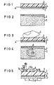
- Figur 1 einen Querschnitt durch eine Ausführungsform eines erfindungsgemäßen Fingerabdruckwandlers;
- Figur 2 eine Draufsicht den in Figur 1 dargestellten Fingerabdruckwandler, wobei eine zufällige Erhebungsverteilung auf der Abtastfläche dargestellt ist;
- Figur 3 den in Figur 1 dargestellten Querschnitt mit einem auf die Abtastfläche gedrückten Finger;
- Figur 4 wieder eine Draufsicht auf den Fingerabdruckwandler nach Figur 1, wobei ein Fingerabdruck auf der Abtastfläche dargestellt ist;
- Figur 5 in vergrößerter Darstellung einen Querschnitt des Fingerabdruckwandlers gemäß Figur 4 mit weggebrochenen Teilen, wobei geriffelte Elemente und an den Stellen, wo der Fingerabdruck gemacht wurde, flache Elemente auf der Abtastfläche gezeigt sind;
Figur 6 eine Anordnung zur Gewinnung oder zum Lessen des Fingerabdrucks;- Figur 7 eine Vorrichtung zum Auslöschen des Fingerabdrucks und zur Wiedergewinnung des räumlich zufälligen Reliefs;
Figur 8 einen Querschnitt durch einen Fingerabdruckwandler; der für eine nächste Überprüfung bereit ist;Figur 9 einen erfindungsgemäßen Fingerabdruckwandler, der mittels einer IR-Lichtquelle erwärmbar ist;- Figur 10 eine Draufsicht auf eine Elektrode, welche in einem erfindungsgemäßen Wandler benutzt werden kann;
- Figur 11 eine perspektivische Darstellung einer Ausführungsform der Erfindung, welche eine gitterförmige Beladungselektrode aufweist; und
- Figur 12 eine perspektivische Darstellung einer anderen Ausführungsform der Erfindung, welche einen einzelnen Draht als Beladungselektrode aufweist.
- 1 shows a cross section through an embodiment of a fingerprint converter according to the invention;
- FIG. 2 shows a plan view of the fingerprint converter shown in FIG. 1, a random elevation distribution being shown on the scanning surface;
- 3 shows the cross section shown in Figure 1 with a finger pressed on the scanning surface;
- FIG. 4 shows a top view of the fingerprint converter according to FIG. 1, a fingerprint being shown on the scanning surface;
- FIG. 5 shows an enlarged illustration of a cross section of the fingerprint transducer according to FIG. 4 with parts broken away, with corrugated elements and flat elements on the scanning surface being shown at the places where the fingerprint was made;
- FIG. 6 shows an arrangement for obtaining or reading the fingerprint;
- FIG. 7 shows a device for erasing the fingerprint and for recovering the spatially random relief;
- FIG. 8 shows a cross section through a fingerprint converter; who is ready for a next review;
- FIG. 9 shows a fingerprint converter according to the invention, which can be heated by means of an IR light source;
- FIG. 10 shows a plan view of an electrode which can be used in a transducer according to the invention;
- FIG. 11 shows a perspective illustration of an embodiment of the invention which has a grid-shaped loading electrode; and
- Figure 12 is a perspective view of another embodiment of the invention, which has a single wire as a loading electrode.
Gemäß der Figur 1 ist als Abtastelement 2 eine rechtwinkelige flache Platte vorgesehen. Das Abtastelement 2 weist eine erste Fläche, genannt Abtastfläche 3,und eine zweite Fläche, genannt untere Fläche 4, auf. Das Abtastelement 2-ist aus Material gefertigt, welches wiederbenutzbar ist, vorzugsweise aus einem elastomerischen oder thermoplastischen Material, beispielsweise plastifiziertes Polystyrol. Das Material des Abtastelements 2 ist elektrisch nicht leitend. Es ist so ausgewählt, daß seine Übergangs- oder Erweichungstemperatur .höher als die das Element zwei umgebende Umgebungstemperatur und in der Nähe der Temperatur des menschlichen Körpers liegt. Insbesondere.sollte die Erweichungstemperatur so gewählt sein, daß sie größer als etwa 40°C ist. Sie kann so gewählt sein, daß sie nur einige wenige Celsiusgrade über der Umgebungstemperatur liegt. Die Abtastfläche 3 ist so ausgebildet, daß sie für eine kurze Zeitdauer den Druck eines in Figur 3 dargestellten, zu untersuchenden Fingers 5 aufnimmt. Allgemein gesprochen ist die Erweichungstemperatur so ausgewählt, daß eine dünne Schicht des Materials der Abtastfläche 3 zu schmelzen beginnt, wenn der Finger 5 draufgedrückt wird. Abweichend von der Darstellung nach Figur 1 braucht die Abtastfläche 3 des Abtastelements 2 nicht flach zu sein. Sie kann auch derartig gekrümmt sein, daß sie dem Umriß des Fingers 5 angepaßt ist.According to FIG. 1, a rectangular flat plate is provided as the scanning element 2. The scanning element 2 has a first surface, called the scanning surface 3, and a second surface, called the lower surface 4. The scanning element 2 is made of material which is reusable, preferably of an elastomeric or thermoplastic material, for example plasticized polystyrene. The material of the scanning element 2 is not electrically conductive. It is selected so that its transition or softening temperature is higher than the ambient temperature surrounding the element and close to the temperature of the human body. In particular, the softening temperature should be selected so that it is greater than about 40 ° C. It can be chosen so that it is only a few degrees Celsius above the ambient temperature. The scanning surface 3 is designed such that it receives the pressure of a finger 5 to be examined shown in FIG. 3 for a short period of time. Generally speaking, the softening temperature is selected so that a thin layer of the material of the scanning surface 3 begins to melt when the finger 5 is pressed onto it. 1, the scanning surface 3 of the scanning element 2 need not be flat. It can also be curved in such a way that it is adapted to the outline of the finger 5.
An der zweiten Fläche 4 ist eine Elektrode 6 angebracht. Die Elektrode 6 ist bevorzugterweise aus einem Material gefertigt, welches im Hinblick auf das Licht eines abfragenden Strahls, der-in den Figuren 5 und 6 angedeutet ist, transparent-ist. Sie kann aus Indiumoxid (In0) gefertigt sein. Die Elektrode 6 ist in der Form einer dünnen rechtwinkeligen Platte oder eines entsprechenden Drahtsystems ausgebildet, oder kann als dünner Filmüberzug ausgebildet sein. Die Elektrode 6 kann geerdet sein. Sie ist von einer lichtdurchlässigen Trägerplatte 7 getragen, beispielsweise von einem Glassubstrat.An
Gemäß den Figuren 1 und 2 weist die Abtastfläche 3 ein Oberflächenrelief zufälliger Konfiguration auf. In anderen Worten ausgedrückt, die Oberfläche 3 enthält viele kleine Erhebungen und/oder Vertiefungen in einer Zufallsverteilung. Diese Variationen in den Erhebungen in oder auf der Fläche, die kein spezielles Muster aufweisen, können vorzugsweise auf eine weiter unten näher beschriebene Art und Weise erzeugt werden. Bei Belichtung der Fläche 3 würden alle Segmente das Licht in einer zufälligen Weise streuen, so daß keine bevorzugte Streurichtung vorläge. Die Erzeugung eines dünnen Oberflächenreliefs zufälliger Konfiguration bildet einen ersten Verfahrensschritt.According to FIGS. 1 and 2, the scanning surface 3 has a surface relief of a random configuration. In other words, the surface 3 contains many small elevations and / or depressions in a random distribution. These variations in the elevations in or on the surface, which have no special pattern, can preferably be generated in a manner described in more detail below. Upon exposure of area 3, all segments would scatter the light in a random manner so that there was no preferred direction of scattering. The creation of a thin surface relief of random configuration forms a first process step.
In einem zweiten Verfahrensschritt wird der Finger 5 gegen die flache Abtastflähe 3 des Abtastelements 2 gedrückt. Dies kann der Figur 3 entnommen werden.In a second method step, the finger 5 is pressed against the flat scanning surface 3 of the scanning element 2. This can be seen in FIG. 3.
Der nächste Verfahrensschritt liegt in der Wegnahme des Fingers 5 von der Abtastfläche 3. Wie in der Figur 4 dargestellt, ist ein Fingerabdruck 8 auf der Fläche 3 zurückgelassen worden. Aufgrund des bzw. der auf die Oberfläche 3 durch die Erhebungen des Fingers ausgeübten Druckes bzw. Temperatur schmilzt das zufällige Oberflächenrelief lokal. In den geschmolzenen Abschnitten existieren keine Erhebungen und keine Vertiefungen mehr. Diese Abschnitte sind "ausgebügelt"; sie bilden jetzt flache Bereiche.The next step in the method is to remove the finger 5 from the scanning surface 3. As shown in FIG. 4, a
Dies ist in der Figur 5 dargestellt. Bereiche oder Abschnitte, in welchen noch eine statistische Verteilung vorhanden ist, sind mit 8a und Bereiche oder Abschnitte, in denen die statistische Verteilung der kleinen Vertiefungen und/oder Erhebungen durch die Erhebungen des Fingers "ausgebügelt"worden sind, sind mit 8b bezeichnet.This is shown in FIG. 5. Areas or sections in which a statistical distribution is still present are designated by 8a and areas or sections in which the statistical distribution of the small depressions and / or elevations have been “ironed out” by the elevations of the finger are designated by 8b.
In den Figuren 5 und 6 ist der nächste Verfahrensschritt dargestellt. In diesem Schritt wird die indem "eingefrorenen" Fingerabdruck enthaltene Information optisch ausgelesen und analysiert. Dies kann mittels des Lichts eines abfragenden oder lesenden Strahls 9 entweder in Transmission oder'in Reflexion ausgeführt werden. Die Ausführungsform nach den Figuren 5 und 6 zeigt ein Auslesen mittels transmittierenden Lichts. Der Strahl 9 wird senkrecht auf die untere Fläche 4 des Abtastelements 2 gerichtet. Zu diesem'Zweck wird der Strahl 9 durch das transparente Element 7 und die transparente Elektrode 6 in das Abtastelement 2 transmittiert. Schließlich erreicht es die obere Fläche 3. Nachdem es den Fingerabdruck 8 passiert hat, trägt es die Fingerabdruckinformation. Das Licht wird entsprechend den Vertiefungen und Erhöhungen der Fläche 3 räumlich moduliert, d.h. es trägt die Information über die geometrische Struktur des Fingerabdrucks 8. Die Analysierung der in dem modulierten Licht enthaltenen Information kann prinzipiell auf irgend eine bekannte Art und Weise ausgeführt werden. In den Figuren 5 und 6 ist jedoch eine sehr einfache Methode veranschaulicht.The next process step is shown in FIGS. 5 and 6. In this step, the information contained in the "frozen" fingerprint is optically read out and analyzed. This can be carried out by means of the light of an interrogating or
In den Abschnitten 8b wird das Licht nur in engen Kegeln 10a gestreut, welche die optische Achse des illuminierenden Strahls umgeben (Vorwärtsstreuung). In den Abschnitten.8a jedoch, in denen die zufällige Verteilung des ursprünglichen Oberflächenreliefs durch die Erhöhungen des berührenden Fingers nicht geändert worden ist, wird der illuminierende Strahl in weit geöffneten Kegeln 10a gestreut. Das bedeutet, daß die geschmolzenen Teile des Elements 2 nicht mehr länger Licht in der gleichen Weise streuen als in der unzerstörten Umgebung. Gemäß Figur 6.kann das Fingerabdruckmuster in Form von dunklen Linien auf einem erleuchteten Hintergrund gesehen werden, wenn die Fläche 3 unter einem spitzen Winkel α relativ zur Normalen gesehen wird. Das Bild der Abtastfläche 3 und das Bild 8' des Fingerabdrucks 8 kann über ein optisches System 11 auf eine lichtempfindliche Vorrichtung 12 gerichtet werden. Diese Vorrichtung 12 kann aus einem Feld aus Fotoelektroden zum Umformen des Bildes in elektrische Signale bestehen. Wie aus der Figur 7 hervorgeht, wird im nächsten Schritt des Verfahrens der Fingerabdrucksensor in seinen ursprünglichen Zustand zurückgesetzt. Dieser Schritt umfaßt eine elektrostatische Aufladung und gleichzeitige Erwärmung. Zu diesem Zweck sind eine Einrichtung zum elektrostatischen Aufladen und eine Heizeinrichtung vorgesehen. Die Einrichtung zum Aufladen umfaßt eine Spannungsquelle 14 mit einer Hochspannung V, die mittels eines Schalters 16 zwischen Masse und einer Elektrode 15 geschaltet werden kann. Die Elektrode 15 ist in einem Abstand von der Abtastfläche 3 angeordnet. Sie wird von einem Trägerelement 17 getragen, beispielsweise von einem Glassubstrat. Die Elektrode 15 kann aus einem einzigen Draht bestehen, der parallel zur Fläche 3 angeordnet ist. In der vorliegenden Ausführungsform besteht sie aus einer planen Elektrode, die.mit der unteren Fläche des Trägerelements 1'7 verbunden ist.In
Sobald der Schalter 16 geschlossen worden ist, bewirkt die Hochspannung V zwischen den Elektroden 6 und 15 eine Ionisierung der in der Nähe der Elektrode 15 befindlichen Luft. Aufgrund der Ionisierung der Luft werden elektrische Ladungen zu der Abtastfläche 3 gelenkt. Diese Ladungen werden auf der Fläche 3 gehalten. Sie können von der Fläche 3 nicht abfließen, weil das Abtastelement 2 einen elektrischen Isolator bildet. Wie ebenfalls in der Figur 7 dargestellt, ist der positive Anschluß der Hochspannungsquelle 14 mit der Elektrode 15 verbunden, während der negative Anschluß mit der Elektrode 6 verbunden ist. Deshalb wird die Fläche 3 mit positiven Teilchen aufgeladen. Eine Aufladung mit negativen Teilchen ist jedoch ebenfalls, möglich. Um eine negative elektrostatische Aufladung zu erhalten, ist es lediglich erforderlich, die Polarität der Hochspannungsquelle 14 in Bezug auf die Elektroden 6 und 15 umzukehren. Wie es in der Figur 7 angedeutet ist, würden sich die positiven Partikel ohne Erwärmung in gewissen Flächenelementen im Bereich des Fingerabdrucks 8 sammeln. Aufgrund der lokal variierenden Ladungsdichte wären unterschiedliche elektrische Feldstärken vorhanden und unterschiedliche elektrische Kräfte würden auf verschiedene Flächenelemente ausgeübt.As soon as the
In der Figur 7 ist auch eine Heizeinrichtung dargestellt, welche in der vorliegenden Ausführungsform elektrischer Natur ist, insbesondere aus einer Widerstands-Heizeinrichtung besteht. Die Heizeinrichtung besteht aus einer Heizstromquelle 18 und einem Schalter 19. Die Heizstromquelle 18 und der Schalter 19 sind zwischen einem Ende der Elektrode 6 und Masse in Serie geschaltet. Das andere Ende der Elektrode 6 ist ebenfalls mit Masse verbunden. Wenn der Schalter 19 geschlossen wird, liefert die Heizstromquelle 18 einen Heizstrom (Gleichstrom oder pulsierenden Strom), der durch die Elektrode 6 fließt. Demgemäß ist die Elektrode 6 nicht nur eine Hochspannungselektrode, die zur -elektrostatischen Aufladung benutzt wird, sie ist zugleich ein Heizwiderstand, beispielsweise ein Widerstandsgitter. Der Heizstrom heizt das Abtastelement 2 auf. Die Größe des Heizstroms ist so gewählt, daß auf der Abtastfläche 3 eine Temperatur erreicht wird, die wenigstens näherungsweise der Erweichungstemperatur des elastomerischen oder thermoplastischen Materials entspricht. Im Laufe des Erwärmungsvorgangs wird die Fläche 3 des Abtastelements 2 weich und beginnt zu schmelzen. Jetzt kann die Fläche 3 flach werden oder sich glätten und der Fingerabdruck 8 wird ausgelöscht. Die elektrostatische Ladung verteilt sich zufällig auf der Fläche, wodurch elektrostatische Kräfte auf die Fläche 3 ausgeübt werden, die eine Zufallsverteilung von Vertiefungen und/ oder Erhebungen zur Folge haben. Die Folge davon ist, daß wieder ein Wandler erhalten wird, der statistische Oberflächeneigenschaften aufweist. Dieser Effekt ist in der Literatur als Frost-Effekt thermoplastischer Medien bekannt.FIG. 7 also shows a heating device which, in the present embodiment, is electrical in nature, in particular consists of a resistance heating device. The heating device consists of a heating
Gemäß Figur 8 liegt der letzte Verfahrensschritt im Abkühlen des Abtastelements 2. Dies kann einfach durch Ausschalten des Schalters 19 erreicht werden, vorausgesetzt, daß die Umgebungstemperatur niedrig genug ist. Zusätzlich kann eine nicht dargestellte Kühleinrichtung an das Abtastelement 2 angeschlossen sein, beispielsweise thermoelektrische Peltier-Elemente. Das Abkühlen des Abtastelements 2 hat ein "Einfrieren" des Zufallmusterreliefs der Fläche 3 zur Folge. Es sei darauf hingewiesen, daß während des Abkühlvorganges die Elektrode 15 von der Hochspannungsquelle 14 abgeschaltet ist. Nach'dem Abkühlen ist das Abtastelement 2 für den nächsten Fingerabdruckvorgang und Lesezyklus. bereit.According to FIG. 8, the last process step is to cool the scanning element 2. This can be achieved simply by switching off the
Aus Figur 9 geht hervor, daß das Erwärmen des Abtastelements 2 (siehe Figur 7) auch mittels einer strahlenden Heizeinrichtung erreicht werden kann. In diesem Fall wird eine IR-Strahlungsquelle 20 benutzt, welche IR-Strahlung 21 in Richtung der unteren Seite der Elektrode 6 sendet. Die IR-Quelle 20 kann eine einzige IR-Quelle oder ein Feld aus einzelnen IR-Quellen sein. Als IR-Quelle 20 kann eine IR-Strahlung imitierende LED oder eine IR-Lampe benutzt werden.It is apparent from FIG. 9 that the heating of the scanning element 2 (see FIG. 7) can also be achieved by means of a radiant heating device. In this case, an
Aus der Figur 10 geht eine Ausführungsform der Elektrode 6 hervor. Die Elektrode 6 kann aus einem Feld paralleler Widerstandsdrähte bestehen. Diese Drähte können sowohl als Elektrode beim elektrostatischen Aufladungsvorgäng als auch als Heizkörper beim Erwärmungsvorgang dienen. In der Figur 11 ist eine perspektivische Darstellung einer anderen Ausführungsform der Erfindung dargestellt. Bei dieser Ausführungsform besteht die Elektrode 15 zum Aufladen der oberen Fläche des Elements aus einem Feld paralleler Dränte, die auf einer Seite an ein Verbindungselement 23 angeschlossen sind, welches seinerseits über den Schalter 1'6 mit der Hochspannungsquelle 14 verbunden ist. Das Feld paralleler Drähte kann durch geeignete Einrichtungen, welche nicht dargestellt sind, gehalten sein.An embodiment of the
In der Figur 12 ist eine perspektivische Darstellung einer noch anderen Ausführungsform der Erfindung gezeigt. Bei dieser Ausführungsform besteht die Elektrode 15 aus einem einzigen Draht, der parallel zur Fläche des Elements 2 gehalten ist'. Die Elektrode 15 ist auf der von der Fläche 3 abgewandten Seite durch einen Schirm 25 abgeschirmt. Deshalb werden geladene Teilchen im wesentlichen zwischen dem Schirm 25 und der oberen Fläche 3 des Abtastelements 2 erzeugt.FIG. 12 shows a perspective illustration of yet another embodiment of the invention. In this embodiment, the
Claims (12)
Applications Claiming Priority (2)
| Application Number | Priority Date | Filing Date | Title |
|---|---|---|---|
| US06/152,513 US4358677A (en) | 1980-05-22 | 1980-05-22 | Transducer for fingerprints and apparatus for analyzing fingerprints |
| US152513 | 1980-05-22 |
Publications (1)
| Publication Number | Publication Date |
|---|---|
| EP0040838A1 true EP0040838A1 (en) | 1981-12-02 |
Family
ID=22543241
Family Applications (1)
| Application Number | Title | Priority Date | Filing Date |
|---|---|---|---|
| EP81103955A Withdrawn EP0040838A1 (en) | 1980-05-22 | 1981-05-22 | Detector and analysing system for fingerprints |
Country Status (2)
| Country | Link |
|---|---|
| US (1) | US4358677A (en) |
| EP (1) | EP0040838A1 (en) |
Cited By (5)
| Publication number | Priority date | Publication date | Assignee | Title |
|---|---|---|---|---|
| WO1996011632A1 (en) * | 1994-10-13 | 1996-04-25 | Central Research Laboratories Limited | Apparatus and method for imaging skin ridges |
| US5828773A (en) * | 1996-01-26 | 1998-10-27 | Harris Corporation | Fingerprint sensing method with finger position indication |
| US5841888A (en) * | 1996-01-23 | 1998-11-24 | Harris Corporation | Method for fingerprint indexing and searching |
| US5862248A (en) * | 1996-01-26 | 1999-01-19 | Harris Corporation | Integrated circuit device having an opening exposing the integrated circuit die and related methods |
| US5963679A (en) * | 1996-01-26 | 1999-10-05 | Harris Corporation | Electric field fingerprint sensor apparatus and related methods |
Families Citing this family (43)
| Publication number | Priority date | Publication date | Assignee | Title |
|---|---|---|---|---|
| US4394773A (en) * | 1980-07-21 | 1983-07-19 | Siemens Corporation | Fingerprint sensor |
| US5222153A (en) * | 1988-09-02 | 1993-06-22 | Thumbscan, Inc. | Apparatus for matching a fingerprint using a tacky finger platen |
| JPH0762865B2 (en) * | 1993-05-13 | 1995-07-05 | 日本電気株式会社 | Fingerprint image input device |
| US7248719B2 (en) | 1994-11-28 | 2007-07-24 | Indivos Corporation | Tokenless electronic transaction system |
| US20040128249A1 (en) | 1994-11-28 | 2004-07-01 | Indivos Corporation, A Delaware Corporation | System and method for tokenless biometric electronic scrip |
| US6950810B2 (en) | 1994-11-28 | 2005-09-27 | Indivos Corporation | Tokenless biometric electronic financial transactions via a third party identicator |
| US7882032B1 (en) | 1994-11-28 | 2011-02-01 | Open Invention Network, Llc | System and method for tokenless biometric authorization of electronic communications |
| US7613659B1 (en) | 1994-11-28 | 2009-11-03 | Yt Acquisition Corporation | System and method for processing tokenless biometric electronic transmissions using an electronic rule module clearinghouse |
| US7631193B1 (en) | 1994-11-28 | 2009-12-08 | Yt Acquisition Corporation | Tokenless identification system for authorization of electronic transactions and electronic transmissions |
| NO951427D0 (en) * | 1995-04-11 | 1995-04-11 | Ngoc Minh Dinh | Method and apparatus for measuring patterns in a partially heat conducting surface |
| US5708497A (en) * | 1995-08-15 | 1998-01-13 | Nec Corporation | Fingerprint image input apparatus and method of producing the same |
| WO1997041527A1 (en) * | 1996-05-01 | 1997-11-06 | Xros, Inc. | Compact, simple, 2d raster, image-building fingerprint scanner |
| FR2755526B1 (en) * | 1996-11-05 | 1999-01-22 | Thomson Csf | FINGERPRINT READING SYSTEM WITH INTEGRATED HEATING RESISTORS |
| JP2962274B2 (en) * | 1997-04-18 | 1999-10-12 | 日本電気株式会社 | Biological identification method and device |
| US6856383B1 (en) | 1997-09-05 | 2005-02-15 | Security First Corp. | Relief object image generator |
| US6501846B1 (en) | 1997-11-25 | 2002-12-31 | Ethentica, Inc. | Method and system for computer access and cursor control using a relief object image generator |
| US6466686B2 (en) * | 1998-01-07 | 2002-10-15 | International Business Machines Corporation | System and method for transforming fingerprints to improve recognition |
| US6131464A (en) * | 1998-06-16 | 2000-10-17 | Smarttouch, Inc. | Pressure sensitive biometric input apparatus |
| US6870946B1 (en) * | 1998-08-06 | 2005-03-22 | Secugen Corporation | Compact optical fingerprint capturing and recognition system |
| US6381347B1 (en) | 1998-11-12 | 2002-04-30 | Secugen | High contrast, low distortion optical acquistion system for image capturing |
| WO2000079214A1 (en) | 1999-06-23 | 2000-12-28 | Johnson Neldon P | Fingerprint sensing device and method |
| US6191410B1 (en) | 1999-06-23 | 2001-02-20 | International Automated Systems, Inc | Fingerprint sensing apparatus and method |
| US6632512B1 (en) * | 1999-11-10 | 2003-10-14 | Ibiden Co., Ltd. | Ceramic substrate |
| US9165323B1 (en) | 2000-05-31 | 2015-10-20 | Open Innovation Network, LLC | Biometric transaction system and method |
| AU2001266628A1 (en) | 2000-05-31 | 2001-12-11 | Indivos Corporation | Biometric financial transaction system and method |
| US7960670B2 (en) * | 2005-05-03 | 2011-06-14 | Kla-Tencor Corporation | Methods of and apparatuses for measuring electrical parameters of a plasma process |
| KR100432490B1 (en) | 2001-09-17 | 2004-05-22 | (주)니트 젠 | Optical fingerprint acquisition apparatus |
| US6809303B2 (en) * | 2001-11-13 | 2004-10-26 | Cross Match Technologies, Inc. | Platen heaters for biometric image capturing devices |
| US6872916B2 (en) * | 2001-11-13 | 2005-03-29 | Cross Match Technologies, Inc. | System and method for biometric image capturing |
| US20030104693A1 (en) * | 2001-11-30 | 2003-06-05 | Siegel Harry M. | Use of fluoropolymer coating for planarizing and passivating integrated circuit devices |
| US6707093B2 (en) * | 2001-11-30 | 2004-03-16 | Stmicroelectronics, Inc. | Selective ionic implantation of fluoropolymer film to modify the sensitivity of underlying sensing capacitors |
| US20050184052A1 (en) * | 2002-01-17 | 2005-08-25 | Cross Match Technologies, Inc. | System and method for biometric image capturing |
| ATE406626T1 (en) | 2002-01-17 | 2008-09-15 | Cross Match Technologies Inc | FINGERPRINT WORKSTATION AND METHOD |
| DE10222616A1 (en) * | 2002-05-17 | 2003-12-04 | Univ Albert Ludwigs Freiburg | Fingerprint verification module |
| US20040125990A1 (en) * | 2002-12-26 | 2004-07-01 | Motorola, Inc. | Method and apparatus for asperity detection |
| US7406185B2 (en) * | 2003-04-16 | 2008-07-29 | Ligh Tuning Technology Inc. | Thermoelectric sensor for fingerprint thermal imaging |
| KR100964559B1 (en) * | 2003-04-25 | 2010-06-21 | 삼성전자주식회사 | Fingerprinting device |
| KR20040105107A (en) * | 2003-06-05 | 2004-12-14 | 현대자동차주식회사 | An apparatus for controlling temperature of a fingerprint sensor for a vehicle |
| US7277562B2 (en) | 2003-08-01 | 2007-10-02 | Cross Match Technologies, Inc. | Biometric imaging capture system and method |
| GB0522461D0 (en) * | 2005-11-03 | 2005-12-14 | Immunoclin Ltd | Dactyl detector |
| TWI456510B (en) * | 2011-08-24 | 2014-10-11 | Gingy Technology Inc | Fingerprint touch panel |
| CA2888468A1 (en) * | 2012-10-17 | 2014-04-24 | Gelsight, Inc. | Three-dimensional digital impression and visualization of objects |
| EP3665616A4 (en) | 2017-08-09 | 2021-06-02 | The Board of Trustees of the Leland Stanford Junior University | Interactive biometric touch scanner |
Citations (5)
| Publication number | Priority date | Publication date | Assignee | Title |
|---|---|---|---|---|
| DE27304C (en) * | C. A. E. FAGERBERG in Stockholm, Schweden | Spring-loaded swivel joint for doors | ||
| GB900068A (en) * | 1960-05-06 | 1962-07-04 | Gen Electric | Method of and apparatus for enhancing the development of deformable storage media |
| US3532426A (en) * | 1967-11-08 | 1970-10-06 | Gen Electric | Holographic fingerprint identification |
| US3533823A (en) * | 1968-02-15 | 1970-10-13 | Ling Temco Vought Inc | Method of making a facsimile of a skin friction-ridge pattern |
| FR2448338A1 (en) * | 1979-02-12 | 1980-09-05 | Energy Conversion Devices Inc | METHOD AND APPARATUS FOR RECORDING THE TOPOLOGY OF A TISSUE SURFACE OF LIVING SKIN |
Family Cites Families (9)
| Publication number | Priority date | Publication date | Assignee | Title |
|---|---|---|---|---|
| BE631983A (en) * | 1962-05-08 | |||
| US3542545A (en) * | 1966-01-13 | 1970-11-24 | Xerox Corp | Frost or relief wrinkling of an imaging article comprising an electrically photosensitive layer and a deformable layer |
| US3660818A (en) * | 1970-05-04 | 1972-05-02 | Rca Corp | Electro-optical memory |
| US3716359A (en) * | 1970-12-28 | 1973-02-13 | Xerox Corp | Cyclic recording system by the use of an elastomer in an electric field |
| US3795514A (en) * | 1972-09-15 | 1974-03-05 | Xerox Corp | Deformation imaging method |
| US3865488A (en) * | 1973-11-30 | 1975-02-11 | Rca Corp | Fingerprint display system utilizing a stored fingerprint |
| US4023969A (en) * | 1975-01-03 | 1977-05-17 | Xerox Corporation | Deformable elastomer imaging member employing an internal opaque deformable metallic layer |
| US4120585A (en) * | 1976-11-19 | 1978-10-17 | Calspan Corporation | Fingerprint identification system using a pliable optical prism |
| US4223062A (en) * | 1978-11-15 | 1980-09-16 | Bell & Howell Company | Curl resistant photoplastic film |
-
1980
- 1980-05-22 US US06/152,513 patent/US4358677A/en not_active Expired - Lifetime
-
1981
- 1981-05-22 EP EP81103955A patent/EP0040838A1/en not_active Withdrawn
Patent Citations (5)
| Publication number | Priority date | Publication date | Assignee | Title |
|---|---|---|---|---|
| DE27304C (en) * | C. A. E. FAGERBERG in Stockholm, Schweden | Spring-loaded swivel joint for doors | ||
| GB900068A (en) * | 1960-05-06 | 1962-07-04 | Gen Electric | Method of and apparatus for enhancing the development of deformable storage media |
| US3532426A (en) * | 1967-11-08 | 1970-10-06 | Gen Electric | Holographic fingerprint identification |
| US3533823A (en) * | 1968-02-15 | 1970-10-13 | Ling Temco Vought Inc | Method of making a facsimile of a skin friction-ridge pattern |
| FR2448338A1 (en) * | 1979-02-12 | 1980-09-05 | Energy Conversion Devices Inc | METHOD AND APPARATUS FOR RECORDING THE TOPOLOGY OF A TISSUE SURFACE OF LIVING SKIN |
Cited By (8)
| Publication number | Priority date | Publication date | Assignee | Title |
|---|---|---|---|---|
| WO1996011632A1 (en) * | 1994-10-13 | 1996-04-25 | Central Research Laboratories Limited | Apparatus and method for imaging skin ridges |
| US5841888A (en) * | 1996-01-23 | 1998-11-24 | Harris Corporation | Method for fingerprint indexing and searching |
| US6181807B1 (en) | 1996-01-23 | 2001-01-30 | Authentec, Inc. | Methods and related apparatus for fingerprint indexing and searching |
| US5828773A (en) * | 1996-01-26 | 1998-10-27 | Harris Corporation | Fingerprint sensing method with finger position indication |
| US5852670A (en) * | 1996-01-26 | 1998-12-22 | Harris Corporation | Fingerprint sensing apparatus with finger position indication |
| US5862248A (en) * | 1996-01-26 | 1999-01-19 | Harris Corporation | Integrated circuit device having an opening exposing the integrated circuit die and related methods |
| US5956415A (en) * | 1996-01-26 | 1999-09-21 | Harris Corporation | Enhanced security fingerprint sensor package and related methods |
| US5963679A (en) * | 1996-01-26 | 1999-10-05 | Harris Corporation | Electric field fingerprint sensor apparatus and related methods |
Also Published As
| Publication number | Publication date |
|---|---|
| US4358677A (en) | 1982-11-09 |
Similar Documents
| Publication | Publication Date | Title |
|---|---|---|
| EP0040838A1 (en) | Detector and analysing system for fingerprints | |
| EP0040836A1 (en) | Detector for fingerprints and method of enhancing them | |
| EP0044489B1 (en) | Finger-print sensor | |
| DE69915648T2 (en) | Beam deflector and scanner | |
| EP0048489B1 (en) | Examination apparatus for a finger-relief | |
| DE102012219187B4 (en) | System for binary classification of elements of interest in a reproducible process | |
| DE3047544C2 (en) | ||
| DE2827074A1 (en) | RECORDING DEVICE | |
| DE2931708C2 (en) | Device for controlling the development of a recording medium | |
| DE3009161C2 (en) | Device for the detection and visualization of infrared rays | |
| DE112017005263T5 (en) | REAL-TIME ACTIVITY MONITORING USING THERMO-TAGS | |
| EP0045916A1 (en) | Fingerprint sensor delivering an output signal corresponding to the fingerprint | |
| DE2212968C3 (en) | Method for recording a deformation image | |
| DE2551792A1 (en) | MEMORY ARRANGEMENT WITH NON-CRYSTALLINE SWITCHING DEVICES | |
| DE2312516A1 (en) | PROCESS FOR INCREASING THE DIFFUSION OF A DEFORMATIVE IMAGE | |
| DE2106274A1 (en) | Method and device for evaluating image information stored on a recording medium in the form of surface deformations | |
| EP0045917B1 (en) | Fingerprint sensor delivering an electric signal | |
| DE3111929C2 (en) | ||
| EP0121904A1 (en) | Pressure imaging system | |
| DE69931575T2 (en) | Test arrangement for electronic memory cards | |
| DE2335230C3 (en) | Electrophotographic recording material for the production of deformation images | |
| DE1549144A1 (en) | Information storage device and method for storing information using the same | |
| DE2061417B2 (en) | Device for generating and deleting deformation images | |
| DE1813073A1 (en) | Light modulating device | |
| DE2007728B2 (en) | METHOD AND DEVICE FOR EVALUATING THE DISTRIBUTION OF THE ELECTRIC CHARGE ON AN ELECTROSTATICALLY CHARGED LAYER |
Legal Events
| Date | Code | Title | Description |
|---|---|---|---|
| PUAI | Public reference made under article 153(3) epc to a published international application that has entered the european phase |
Free format text: ORIGINAL CODE: 0009012 |
|
| AK | Designated contracting states |
Designated state(s): AT BE CH DE FR GB IT NL SE |
|
| 17P | Request for examination filed |
Effective date: 19811028 |
|
| STAA | Information on the status of an ep patent application or granted ep patent |
Free format text: STATUS: THE APPLICATION IS DEEMED TO BE WITHDRAWN |
|
| 18D | Application deemed to be withdrawn |
Effective date: 19841112 |
|
| RIN1 | Information on inventor provided before grant (corrected) |
Inventor name: RUELL, HARTWIG, DR. Inventor name: FEIX, WOLFGANG |