CN100534806C - Optically variable element comprising a sequence of thin-film layers - Google Patents
Optically variable element comprising a sequence of thin-film layers Download PDFInfo
- Publication number
- CN100534806C CN100534806C CNB038107724A CN03810772A CN100534806C CN 100534806 C CN100534806 C CN 100534806C CN B038107724 A CNB038107724 A CN B038107724A CN 03810772 A CN03810772 A CN 03810772A CN 100534806 C CN100534806 C CN 100534806C
- Authority
- CN
- China
- Prior art keywords
- layer
- thin
- variable element
- film component
- light variable
- Prior art date
- Legal status (The legal status is an assumption and is not a legal conclusion. Google has not performed a legal analysis and makes no representation as to the accuracy of the status listed.)
- Expired - Fee Related
Links
- 239000010409 thin film Substances 0.000 title claims abstract description 70
- 229910052751 metal Inorganic materials 0.000 claims description 35
- 239000002184 metal Substances 0.000 claims description 35
- 239000010408 film Substances 0.000 claims description 18
- 230000005540 biological transmission Effects 0.000 claims description 16
- 239000002519 antifouling agent Substances 0.000 claims description 15
- 230000000694 effects Effects 0.000 claims description 15
- 230000008859 change Effects 0.000 claims description 8
- 230000000007 visual effect Effects 0.000 claims description 8
- 230000002452 interceptive effect Effects 0.000 claims description 7
- 238000003475 lamination Methods 0.000 claims description 5
- 238000004049 embossing Methods 0.000 claims description 4
- 210000004276 hyalin Anatomy 0.000 claims 2
- 239000011888 foil Substances 0.000 abstract description 7
- 239000010410 layer Substances 0.000 description 353
- 239000000463 material Substances 0.000 description 23
- 238000000034 method Methods 0.000 description 21
- 239000002253 acid Substances 0.000 description 20
- 238000005530 etching Methods 0.000 description 17
- 230000003287 optical effect Effects 0.000 description 12
- 239000011248 coating agent Substances 0.000 description 11
- 238000000576 coating method Methods 0.000 description 11
- 238000001704 evaporation Methods 0.000 description 11
- 230000008020 evaporation Effects 0.000 description 11
- 230000008901 benefit Effects 0.000 description 10
- 230000008569 process Effects 0.000 description 10
- 238000002679 ablation Methods 0.000 description 9
- 238000004519 manufacturing process Methods 0.000 description 7
- 239000011247 coating layer Substances 0.000 description 6
- 238000007639 printing Methods 0.000 description 6
- PXHVJJICTQNCMI-UHFFFAOYSA-N Nickel Chemical compound [Ni] PXHVJJICTQNCMI-UHFFFAOYSA-N 0.000 description 5
- 239000004922 lacquer Substances 0.000 description 5
- 238000001465 metallisation Methods 0.000 description 5
- 230000001681 protective effect Effects 0.000 description 5
- XEEYBQQBJWHFJM-UHFFFAOYSA-N Iron Chemical compound [Fe] XEEYBQQBJWHFJM-UHFFFAOYSA-N 0.000 description 4
- 238000005516 engineering process Methods 0.000 description 4
- 239000000758 substrate Substances 0.000 description 4
- PNEYBMLMFCGWSK-UHFFFAOYSA-N Alumina Chemical compound [O-2].[O-2].[O-2].[Al+3].[Al+3] PNEYBMLMFCGWSK-UHFFFAOYSA-N 0.000 description 3
- 229910052804 chromium Inorganic materials 0.000 description 3
- 239000011651 chromium Substances 0.000 description 3
- 239000012528 membrane Substances 0.000 description 3
- 229910052759 nickel Inorganic materials 0.000 description 3
- 239000004033 plastic Substances 0.000 description 3
- 229920003023 plastic Polymers 0.000 description 3
- VYZAMTAEIAYCRO-UHFFFAOYSA-N Chromium Chemical compound [Cr] VYZAMTAEIAYCRO-UHFFFAOYSA-N 0.000 description 2
- UQSXHKLRYXJYBZ-UHFFFAOYSA-N Iron oxide Chemical compound [Fe]=O UQSXHKLRYXJYBZ-UHFFFAOYSA-N 0.000 description 2
- KDLHZDBZIXYQEI-UHFFFAOYSA-N Palladium Chemical compound [Pd] KDLHZDBZIXYQEI-UHFFFAOYSA-N 0.000 description 2
- VYPSYNLAJGMNEJ-UHFFFAOYSA-N Silicium dioxide Chemical compound O=[Si]=O VYPSYNLAJGMNEJ-UHFFFAOYSA-N 0.000 description 2
- 229910052782 aluminium Inorganic materials 0.000 description 2
- 229910052802 copper Inorganic materials 0.000 description 2
- 239000010949 copper Substances 0.000 description 2
- 238000009760 electrical discharge machining Methods 0.000 description 2
- 229910052737 gold Inorganic materials 0.000 description 2
- 239000010931 gold Substances 0.000 description 2
- 238000010849 ion bombardment Methods 0.000 description 2
- 229910052742 iron Inorganic materials 0.000 description 2
- 238000000608 laser ablation Methods 0.000 description 2
- PQXKHYXIUOZZFA-UHFFFAOYSA-M lithium fluoride Chemical compound [Li+].[F-] PQXKHYXIUOZZFA-UHFFFAOYSA-M 0.000 description 2
- 238000000465 moulding Methods 0.000 description 2
- 239000003973 paint Substances 0.000 description 2
- WXZMFSXDPGVJKK-UHFFFAOYSA-N pentaerythritol Chemical compound OCC(CO)(CO)CO WXZMFSXDPGVJKK-UHFFFAOYSA-N 0.000 description 2
- 239000000049 pigment Substances 0.000 description 2
- 238000007493 shaping process Methods 0.000 description 2
- 229910052709 silver Inorganic materials 0.000 description 2
- IRPGOXJVTQTAAN-UHFFFAOYSA-N 2,2,3,3,3-pentafluoropropanal Chemical compound FC(F)(F)C(F)(F)C=O IRPGOXJVTQTAAN-UHFFFAOYSA-N 0.000 description 1
- KLZUFWVZNOTSEM-UHFFFAOYSA-K Aluminum fluoride Inorganic materials F[Al](F)F KLZUFWVZNOTSEM-UHFFFAOYSA-K 0.000 description 1
- OKTJSMMVPCPJKN-UHFFFAOYSA-N Carbon Chemical compound [C] OKTJSMMVPCPJKN-UHFFFAOYSA-N 0.000 description 1
- RYGMFSIKBFXOCR-UHFFFAOYSA-N Copper Chemical compound [Cu] RYGMFSIKBFXOCR-UHFFFAOYSA-N 0.000 description 1
- ZOKXTWBITQBERF-UHFFFAOYSA-N Molybdenum Chemical compound [Mo] ZOKXTWBITQBERF-UHFFFAOYSA-N 0.000 description 1
- BQCADISMDOOEFD-UHFFFAOYSA-N Silver Chemical compound [Ag] BQCADISMDOOEFD-UHFFFAOYSA-N 0.000 description 1
- UCKMPCXJQFINFW-UHFFFAOYSA-N Sulphide Chemical compound [S-2] UCKMPCXJQFINFW-UHFFFAOYSA-N 0.000 description 1
- RTAQQCXQSZGOHL-UHFFFAOYSA-N Titanium Chemical compound [Ti] RTAQQCXQSZGOHL-UHFFFAOYSA-N 0.000 description 1
- 230000009471 action Effects 0.000 description 1
- 230000003044 adaptive effect Effects 0.000 description 1
- 239000012790 adhesive layer Substances 0.000 description 1
- 239000000956 alloy Substances 0.000 description 1
- 229910045601 alloy Inorganic materials 0.000 description 1
- AZDRQVAHHNSJOQ-UHFFFAOYSA-N alumane Chemical group [AlH3] AZDRQVAHHNSJOQ-UHFFFAOYSA-N 0.000 description 1
- 239000004411 aluminium Substances 0.000 description 1
- XAGFODPZIPBFFR-UHFFFAOYSA-N aluminium Chemical compound [Al] XAGFODPZIPBFFR-UHFFFAOYSA-N 0.000 description 1
- 201000009310 astigmatism Diseases 0.000 description 1
- OYLGJCQECKOTOL-UHFFFAOYSA-L barium fluoride Chemical compound [F-].[F-].[Ba+2] OYLGJCQECKOTOL-UHFFFAOYSA-L 0.000 description 1
- 229910001632 barium fluoride Inorganic materials 0.000 description 1
- 229910052799 carbon Inorganic materials 0.000 description 1
- 150000004770 chalcogenides Chemical class 0.000 description 1
- 239000003795 chemical substances by application Substances 0.000 description 1
- 229910017052 cobalt Inorganic materials 0.000 description 1
- 239000010941 cobalt Substances 0.000 description 1
- GUTLYIVDDKVIGB-UHFFFAOYSA-N cobalt atom Chemical compound [Co] GUTLYIVDDKVIGB-UHFFFAOYSA-N 0.000 description 1
- 239000000470 constituent Substances 0.000 description 1
- 238000010276 construction Methods 0.000 description 1
- 238000000151 deposition Methods 0.000 description 1
- 239000003292 glue Substances 0.000 description 1
- PCHJSUWPFVWCPO-UHFFFAOYSA-N gold Chemical compound [Au] PCHJSUWPFVWCPO-UHFFFAOYSA-N 0.000 description 1
- 238000005286 illumination Methods 0.000 description 1
- 230000006872 improvement Effects 0.000 description 1
- ORUIBWPALBXDOA-UHFFFAOYSA-L magnesium fluoride Chemical compound [F-].[F-].[Mg+2] ORUIBWPALBXDOA-UHFFFAOYSA-L 0.000 description 1
- 229910001635 magnesium fluoride Inorganic materials 0.000 description 1
- 239000011159 matrix material Substances 0.000 description 1
- 150000002739 metals Chemical class 0.000 description 1
- 229910052750 molybdenum Inorganic materials 0.000 description 1
- 239000011733 molybdenum Substances 0.000 description 1
- 230000003647 oxidation Effects 0.000 description 1
- 238000007254 oxidation reaction Methods 0.000 description 1
- 238000012856 packing Methods 0.000 description 1
- 229910052763 palladium Inorganic materials 0.000 description 1
- 238000007747 plating Methods 0.000 description 1
- 238000003672 processing method Methods 0.000 description 1
- 238000002310 reflectometry Methods 0.000 description 1
- 230000010076 replication Effects 0.000 description 1
- 230000000630 rising effect Effects 0.000 description 1
- 238000000926 separation method Methods 0.000 description 1
- 239000000377 silicon dioxide Substances 0.000 description 1
- 239000004332 silver Substances 0.000 description 1
- 239000010944 silver (metal) Substances 0.000 description 1
- 238000010572 single replacement reaction Methods 0.000 description 1
- 238000002910 structure generation Methods 0.000 description 1
- 239000000126 substance Substances 0.000 description 1
- 239000010936 titanium Substances 0.000 description 1
- 229910052719 titanium Inorganic materials 0.000 description 1
- WFKWXMTUELFFGS-UHFFFAOYSA-N tungsten Chemical compound [W] WFKWXMTUELFFGS-UHFFFAOYSA-N 0.000 description 1
- 229910052721 tungsten Inorganic materials 0.000 description 1
- 239000010937 tungsten Substances 0.000 description 1
- 238000005406 washing Methods 0.000 description 1
Images


Classifications
-
- B—PERFORMING OPERATIONS; TRANSPORTING
- B42—BOOKBINDING; ALBUMS; FILES; SPECIAL PRINTED MATTER
- B42D—BOOKS; BOOK COVERS; LOOSE LEAVES; PRINTED MATTER CHARACTERISED BY IDENTIFICATION OR SECURITY FEATURES; PRINTED MATTER OF SPECIAL FORMAT OR STYLE NOT OTHERWISE PROVIDED FOR; DEVICES FOR USE THEREWITH AND NOT OTHERWISE PROVIDED FOR; MOVABLE-STRIP WRITING OR READING APPARATUS
- B42D25/00—Information-bearing cards or sheet-like structures characterised by identification or security features; Manufacture thereof
- B42D25/30—Identification or security features, e.g. for preventing forgery
- B42D25/328—Diffraction gratings; Holograms
-
- B—PERFORMING OPERATIONS; TRANSPORTING
- B42—BOOKBINDING; ALBUMS; FILES; SPECIAL PRINTED MATTER
- B42D—BOOKS; BOOK COVERS; LOOSE LEAVES; PRINTED MATTER CHARACTERISED BY IDENTIFICATION OR SECURITY FEATURES; PRINTED MATTER OF SPECIAL FORMAT OR STYLE NOT OTHERWISE PROVIDED FOR; DEVICES FOR USE THEREWITH AND NOT OTHERWISE PROVIDED FOR; MOVABLE-STRIP WRITING OR READING APPARATUS
- B42D25/00—Information-bearing cards or sheet-like structures characterised by identification or security features; Manufacture thereof
- B42D25/20—Information-bearing cards or sheet-like structures characterised by identification or security features; Manufacture thereof characterised by a particular use or purpose
- B42D25/21—Information-bearing cards or sheet-like structures characterised by identification or security features; Manufacture thereof characterised by a particular use or purpose for multiple purposes
-
- B—PERFORMING OPERATIONS; TRANSPORTING
- B41—PRINTING; LINING MACHINES; TYPEWRITERS; STAMPS
- B41M—PRINTING, DUPLICATING, MARKING, OR COPYING PROCESSES; COLOUR PRINTING
- B41M3/00—Printing processes to produce particular kinds of printed work, e.g. patterns
- B41M3/14—Security printing
-
- B—PERFORMING OPERATIONS; TRANSPORTING
- B42—BOOKBINDING; ALBUMS; FILES; SPECIAL PRINTED MATTER
- B42D—BOOKS; BOOK COVERS; LOOSE LEAVES; PRINTED MATTER CHARACTERISED BY IDENTIFICATION OR SECURITY FEATURES; PRINTED MATTER OF SPECIAL FORMAT OR STYLE NOT OTHERWISE PROVIDED FOR; DEVICES FOR USE THEREWITH AND NOT OTHERWISE PROVIDED FOR; MOVABLE-STRIP WRITING OR READING APPARATUS
- B42D25/00—Information-bearing cards or sheet-like structures characterised by identification or security features; Manufacture thereof
- B42D25/20—Information-bearing cards or sheet-like structures characterised by identification or security features; Manufacture thereof characterised by a particular use or purpose
- B42D25/29—Securities; Bank notes
-
- G—PHYSICS
- G07—CHECKING-DEVICES
- G07D—HANDLING OF COINS OR VALUABLE PAPERS, e.g. TESTING, SORTING BY DENOMINATIONS, COUNTING, DISPENSING, CHANGING OR DEPOSITING
- G07D7/00—Testing specially adapted to determine the identity or genuineness of valuable papers or for segregating those which are unacceptable, e.g. banknotes that are alien to a currency
- G07D7/06—Testing specially adapted to determine the identity or genuineness of valuable papers or for segregating those which are unacceptable, e.g. banknotes that are alien to a currency using wave or particle radiation
- G07D7/12—Visible light, infrared or ultraviolet radiation
-
- B42D2035/24—
Abstract
The invention relates to an optically variable element, in particular an optically variable security element for safeguarding banknotes, credit cards or similar, in addition to a security product and a foil, in particular a stamped foil or a laminated foil comprising an optically variable element of this type. The optically variable element has a thin-film layer (54, 55, 58) for creating colour shifts by means of interference and an additional layer (51, 52, 53, 59). The thin-film is configured as a partial thin-film element, which covers only certain regions of the surface area of the additional layer, forming a pattern.
Description
The present invention relates to a kind of smooth variable element, in particular for the variable protective element of light of protection bank note, credit card and analog, it has one to be used for by the film of interfering the generation colour switching.The invention further relates to a kind of Protection Product and a kind of paper tinsel, especially an embossing film or the lamination paper tinsel with this smooth variable element.
The light variable element usually is used to make file or product to be difficult to duplicate and misapply, and if possible, prevents that also this class incident from taking place.The light variable element usually is used for protected file, bank note, credit card, cash card and analog.
In order to make it to be difficult to duplicate the light variable element, know that make the light variable element have thin layer series, the latter produces the colour switching relevant with the visual angle by interfering.
Described a kind of Protection Product in WO 01/03945A1, it has a transparent substrate, scribbles film on the one side, and this film produces a noticeable colour switching relevant with the visual angle.Film comprises an absorbed layer and a dielectric layer, and the former is coated on the transparent substrate, and the latter is coated on the absorbed layer.Absorbed layer comprises by the combination of a kind of or these materials in the following material to be made: chromium, nickel, palladium, titanium, cobalt, iron, tungsten, molybdenum, iron oxide or carbon.Dielectric layer is made by the combination of a kind of or following material in the following material: silica, aluminium oxide, magnesium fluoride, aluminum fluoride, barium fluoride, calcirm-fluoride or lithium fluoride.
In order further to improve anti-levels of replication, at the side pressure seal diffraction pattern opposite of transparent substrate with thin layer series.This diffraction pattern plays a part diffraction grating, so these two-dimensional patterns allow the observer produce a kind of illusion of 3-D view.
Further suggestion, the side pressure seal diffraction pattern at transparent substrate also is coated with thin layer thereon.
These two forms of implementation by the light variable element can accomplish, in each place of light variable element, optical effect that produces by thin layer and the optical effect that produces by diffraction pattern are overlapping, produce one thus jointly and are difficult to the optical effect of imitating and duplicating.
The present invention is now from the light variable element described in the WO 02/00445A1 that coexists.
Herein, the light variable element is formed by a plurality of layers, and they are placed up and down usually overlappingly.The light variable element has a film on the one hand, and the latter has produced the optical effect of the color change relevant with the visual angle of explanation in the above.In addition, this light variable element has a duplicating layer (Replizierschicht), and wherein impression has embossment structure.This embossment structure produces another optical effect, and the diffraction effect of having said above just by this diffraction effect, can illustrate hologram and analog., will at first on duplicating layer, be coated with on the manufacturing technology herein, impress with embossment structure then with thin layer.
To this, another kind of scheme is separated from each other by the optical effect of membrane structure generation and the optical effect that produces by embossment structure for to describe in WO 02/00445A1.To this, advise two kinds of processing methods.
Suggestion on the one hand is coated with opaque layer between the film of embossment structure that produces holographic picture by diffraction and generation color change.By this opaque layer, embossment structure is shielded by membrane structure.Second possibility is to arrange two or more layers of making of the material of substantially transparent between embossment structure that produces holographic picture by diffraction and thin layer.These layers can comprise one or more high refracting layers and a glue-line.By these layers, can in the embossment structure that produces holographic picture, improve reflectivity, thereby improve luminous intensity.
Herein, can this smooth variable element of following manufacturing: imprinted pattern on a holographic foil at first.A metal level is set to the subregion after this paper tinsel.After this, each thin layer of vapour plating successively.At last, be coated with metal level with full surface.
Another kind of possibility is to be provided with one and to have the prefabricated thin layer series of printable lacquer, and paint the impression embossment structure at this then.Also suggestion in addition, this thin layer of making in advance can glue with prefabricated microstructure.
WO 02/00445A1 describes like this, or the protective element that adopts the optical effect that wherein produces to combine, or adopt wherein optical effect that produces by diffraction structure and the protective element that separates by the optical effect of thin layer generation with the optical effect that produces by membrane structure by diffraction structure.
Now, the present invention promptly, makes the imitation of light variable element and duplicates the difficulty that becomes, and improve the false proof reliability of Protection Product thus based on such task.
This task will be by a smooth variable element; the variable protective element of light in particular for protection bank note, credit card and analog solves; it has thin layer series and other layer that produces the colour switching relevant with the visual angle by interfering; wherein; thin layer series constitutes subregion ground only covers the surface region of other layer by pattern form part thin-film component; described thin layer series has an absorbed layer and transparent λ/4 or λ/2 spacing layers, and perhaps described thin layer series has a plurality of layers with different refractivity.This task also further solves by a Protection Product and a paper tinsel, especially solves by an embossing film or the lamination paper tinsel with a this smooth variable element.
Can obtain such benefit by the present invention, promptly more be difficult to duplicate than the light variable element of knowing by prior art according to smooth variable element of the present invention.Thus, improve the false proof reliability have according to the Protection Product of the light variable element of configuration of the present invention widely., particularly compare with the surface element of building by sandwich-type, false proof reliability improves widely herein.
Like this, the light variable element of for example describing in WO 02/00445A1 (as described in conduct manufacturing possibility in WO02/00445A1) can be imitated thus, promptly process a prefabricated thin film foil, on thin film foil, impress out a diffraction structure with this making ide with a making ide.This in according to the light variable element of configuration of the present invention no longer may: partly be coated with by the thin layer series that interfere to produce colour switching and require to have high technical fee.Compare with prefabricated thin film foil, so the thin-film component of the part that produces is the element of a personalization, so that no longer may imitate the light variable element from the thin layer series of making in advance.
Other advantage of independent expression up to now or surface element stacked on top of each other is preferably optically to be made of one with the tuneable preferably selection (burn into intermediate layer adhesion etc.) of the physical and chemical performance of the autotelic geometrical arrangements of the whole element that will protect, functional window (machine readable, personal data etc.) and the discrete component partly arranged.
Aforementioned other layer be a common protective paint layer, a common reflecting layer or a common glue-line preferably.But, do not need to make the whole surface region of other layer covering light variable element.Remove beyond other layer, additional other layer also can be set, its surface region is subregion ground and covered by thin-film component partly by the shape of pattern only.Also for example can make the light variable element that one common protective paint layer, a common reflecting layer and a common glue-line are arranged.
Reasonably be that the thin-film component of part is made of an absorbed layer and a spacing layer.The thin-film component of part is made of the layer that has different refractivity in a large number each other.
Can further improve false proof reliability thus, promptly Bu Fen thin-film component has a reflecting layer to be preferably a metal level.The identifiability of thin-film component that thus can improvement part.
Another kind of scheme is, also has such possibility, and promptly Bu Fen thin-film component is provided with transmission layer.In the case, particularly advantageously be, this transmission layer is painted, thereby an additional warning sign is provided.
Further may on the thin-film component of part, diffraction structure be set, with as the protective element that adds.Diffraction effect can be for example reached by this diffraction structure, the colour effect of hologram for example or regulation can be produced by this effect.
The imitation of light variable element can further become difficulty thus, and the reflecting layer metal level especially of part promptly is set on the thin-film component of part, and this reflecting layer is the surface region of the thin-film component of cover part partly only.Except related false proof reliability improves therewith, also allow to obtain in this way the decorative effect of being interested in.Can enlarge thus for the employed shape of the structure of light variable element and select.
This advantage can also so reach, and the diffraction structure of part promptly is set in the thin-film component of part, and the latter is the surface region of the thin-film component of part cover part only.
These two measures, just the diffraction structure of Bu Fen reflecting layer and part also can be carried out abreast.
Advantage on a kind of and the manufacturing technology is related, structure by the possibility of the surface region of the light variable element of the thin-film component gauge of part is, is coated with in this surface with an absorbed layer, but does not have the spacing layer.These advantages can also further so obtain, and promptly wherein are coated with the spacing layer in the surface region of light variable element by the thin-film component gauge of part, but do not have absorbed layer.
Such possibility is further arranged, promptly in the surface region by thin-film component gauge partly of light variable element, be coated with one or more replacement layers the film of latter's thin-film component of instead of part in these surface regions.Preferably, these surface regions by the thin-film component gauge of part are surrounded or surround this thin-film component by the thin-film component of part.These measures propose extra high requirement to manufacture process.Correspondingly, make it to be difficult to imitate the light variable element of configuration like this, and improve false proof reliability thus.
The advantage of following layer structure can so obtain, and total bed thickness of promptly one or more replacement layers almost is equivalent to the bed thickness of the thin-film component of part.
It is difficult that the imitation of light variable element can further so become, and one in promptly one or more replacement layers is provided with a diffraction structure.This advantage will further so reach, promptly be coated with a reflecting layer and a supporting course, with instead the layer.Another kind of scheme is, can also be coated with single replacement layer, and the latter can for example relate to a reflecting layer.As what will further illustrate below, this action can be relevant with the advantage on the manufacturing technology.
As illustrated about the thin-film component of part, for the one or more replacement layers of structure also advantageously, the layer of a partial reflection is set, this layer only partly covers one or more surface regions that replace layer.Except the raising of relevant therewith false proof reliability, can also obtain in this way the incorporate interesting decorative effect of Protection Product.The shape that relates to the configuration of light variable element is selected and can be strengthened at this point.These advantages are further to reach thus, some diffraction structure of promptly one or more replacement layers, and the latter partly covers one or more surface regions that replace layer.
Also configuration element " thin-film component of part with layer of partial reflection ", " thin-film component of part with diffraction structure of part ", " the replacement layer with reflecting layer of part " and " the replacement layer with diffraction structure of part " at random can be made up each other.Thus, a kind of can have the combination of many valuable protection characteristics according to smooth variable element of the present invention, and many noticeable structure characteristics are provided.
Below with reference to a plurality of embodiment and by accompanying drawing the present invention is described as an example.
Fig. 1 illustrates the cutaway view by a smooth variable element.
Fig. 2 a illustrates the according to the invention smooth variable element according to the first embodiment of the present invention.
Fig. 2 b illustrates the according to the invention smooth variable element according to the second embodiment of the present invention.
Fig. 2 c illustrates the according to the invention smooth variable element according to the third embodiment of the present invention.
Fig. 3 illustrates the cutaway view by the smooth variable element according to the invention that is used for another embodiment of the present invention.
Fig. 4 illustrates the cutaway view by the smooth variable element according to the invention that is used for another embodiment of the present invention.
Fig. 5 a illustrates the cutaway view by the smooth variable element according to the invention that is used for another embodiment of the present invention.
Fig. 5 b illustrates the cutaway view by the smooth variable element according to the invention that is used for another embodiment of the present invention.
Fig. 5 c illustrates the cutaway view by the smooth variable element according to the invention that is used for another embodiment of the present invention.
Fig. 6 a illustrates the cutaway view by the smooth variable element according to the invention that is used for another embodiment of the present invention.
Fig. 6 b illustrates the cutaway view by the smooth variable element according to the invention that is used for another embodiment of the present invention.
Fig. 7 illustrates the cutaway view by the smooth variable element according to the invention that is used for another embodiment of the present invention.
Fig. 8 illustrates the cutaway view by the smooth variable element according to the invention that is used for another embodiment of the present invention.
Fig. 1 illustrates the principle structure of a smooth variable element O.
Light variable element O decision is used in Protection Product for example on bank note, credit card, cash card or the file.Such possibility is further arranged, i.e. light variable element decision is attached to an object for example on CD or the packing as protection mark or genuine piece mark.
Light variable element O can take many different shapes.Light variable element O can for example be a guard wire.On the object of its intention top loading regulation.
Fig. 1 illustrates a carrier 1 and five layers 2 to 6.Light variable element O is formed by layer 2 to 6.Layer 2 is a protective paint layer and/or separating layer, and layer 3 is an absorbed layer, and layer 4 is a spacing layer.Layer 5 is a metal level or a HRI (high index of refraction) layer.Layer 6 is a glue-line.
Be that layer 2 has an adhesive layer under the situation of a part of lamination paper tinsel at light variable element O.
On principle, the unique distinction of film is to produce the interference layer structure of the colour switching relevant with the visual angle.It can be used as reflecting element and builds, and has the metal level of for example high reflection, or builds as transmissive element, has transparent light separating layer with respect to adjacent layer and (bigger refractive index (HRI) or less refractive index (LRI) is arranged.The matrix of film be configured with an absorbed layer (30% to 65% transmission is preferably arranged), as the transparent spacing layer (for example 1/4th λ layers or 1/2nd λ layers) of the layer that produces color change and as the metal level in reflecting layer or as the light separating layer of transmission layer.
Layer 5 by a reflecting layer for example aluminium form, thereby the bed thickness of spacing layer 4 will so select, and promptly satisfies the condition of λ/4.If layer 5 is made up of a transmission layer, then spacing layer 4 will satisfy the condition of λ/2.
The thin-film component of part is made of a series of high refracting layer and forming low-refractive-index layer.For example, Bu Fen thin-film component constitutes by 3~9 such layers (quantity of thin layer is odd number) or by 2~10 such layers (quantity of thin layer is even number).The number of plies is many more, and the wavelength regulation that then is used for the color change effect is sensitive more.
The example of the bed thickness of each layer of the thin-film component of part and the examples of material that can be used for the thin-film component of part in principle all disclose at the 5th page of WO 01/03945 the 30th the 5th row that walks to the 8th page.
Layer 5 can constitute metal level or HRI layer gross area or the conduct part.Can consider for example combination of Al, Ag, Cr, Ni, Cu, Au or reflective metals as the material that is used for layer 5.
Further can also make layer 5 that a structurized surface is arranged.It can be a diffraction structure, a refraction structure (lens) or macrostructure (greater than 30 μ m).It can also further have a non-structured surface reflective or astigmatism.
Can also remove in principle shown in Fig. 1 the layer in one or more.In addition, light variable element O can also have other one or more layers.
Fig. 2 a to Fig. 2 c illustrates three light variable elements 10,20 and 30.Light variable element 10 has three surface regions 11 to 13, and light variable element 20 has three surface regions 21 to 23, and light variable element 30 then has three surface regions 31 to 33.
Light variable element 10,20 and 30 surface region 12,23 and 31 are covered by the thin-film component of a part separately.As finding out from Fig. 2 a to 2c, thin-film component is subregion ground and constitute as pattern form separately.
The thin-film component of separately part might be made transmission or reflection herein.By the part in surface region separately, pattern shape, be transmission and configuration reflection simultaneously, can reach further interesting effect.In addition, surface region 12,23 and 31 also can be provided with diffraction structure.
Metallisings of light variable element 10,20 and 30 surface region 11,22 and 33 each personal part cover.These surface regions also can be provided with diffraction structure.
In the surface region 13,21 and 32 of light variable element 10,20 and 30, can see a transparent window separately.This transparent window each has the transparent element of part.They have performance transparent or transmission (transparent paint part, organic and inorganic constituents oxidation, partially metallised, the scattering transmission).These surface regions also can be provided with diffraction structure.
Be stressed that, all alignment ground enforcement mutually of the arrangements of elements that schematically illustrates among Fig. 2 a to 2c, and do not limit its generality, can comprise pictorial picture element, alphanumeric symbol and geometrical symbol, bar code and random pattern and their combination simultaneously.
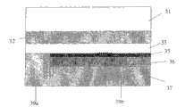
Fig. 3 illustrates a kind of possible mode of construction one smooth variable element, and this element is provided with the thin-film component of a part.
Fig. 3 illustrates a carrier 31, five layers 32 to 37 and two surface region 39a and 39b.
In order to make these layers structure, on carrier 31, be coated with protective paint layer and separating layer 32, duplicating layer 33 and metal level 35 gross area.By coining tool layer 35 partly is provided with diffraction structure then.Then use resistance to acid attack thing stamp on metal level 35, so that metal level only partly forms the layer 36 that is shaped.
Next remove the surface that is not covered by acid etching by the resistance to acid attack thing.
Another kind of scheme is, metal level 35 can also remove or non-metallic by ablation method such as laser ablation, spark erosion, plasma bombardment or ion bombardment.By this ablation method, can also shift image, text and code that digitlization stores.
In the intermediate space that between the layer 35 and 36 of part, constitutes, only introduce the thin-film component of part.Each layer of the thin-film component of part herein can be in the zone of intermediate space evaporation mask by relative configurations carry out evaporation or use by the printing of layer.
Further can also be as shown in Figure 3, the subregion of intermediate space is not covered by the thin-film component of part, thereby produces a transparent window.When being coated with glue-line, then as shown in Figure 3, glue-line correspondingly is shaped thicklyer herein.
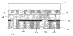
Fig. 4 illustrates a smooth variable element, and wherein, the surface region by thin-film component gauge partly of light variable element has a spacing layer, but does not have absorbed layer.
Fig. 4 illustrates a carrier 41, five layers 42 to 47 and a plurality of surface region 49a and 49b.
In order to make these layers structure, on carrier 41, be coated with protective paint layer and separating layer 42 and absorbed layer 43 gross area.Absorbed layer 43 can be coated with up with vapour deposition method or by printing process herein.
Then in surface region 49b, partly remove absorbed layer.
Removing by positive acid etching or negative acid etching of the part of absorbed layer undertaken.Like this, when direct acid etching, can for example be coated with etching agent as diaphragm by print process by roller or by serigraphy.In addition, also can be coated with the acid etching diaphragm, this diaphragm removes by washing process after the acid etching process.
Further can also be by ablation method such as laser ablation, spark erosion, plasma bombardment or ion bombardment removing absorbed layer.By this ablation method, can also shift image, text and code that digitlization stores.
Also can only partly on layer 42, be coated with absorbed layer, to be coated with absorbed layer with replacing gross area.This can be on layer 42 by realizing by printing by the evaporation of the evaporation mask of pattern form structure or the corresponding pattern form by absorbed layer 43.
Just can on the absorbed layer 43 that partly is shaped, be coated with spacing layer 44 now gross area.The coating of spacing layer can for example be passed through evaporation or pass through the printing realization of the gross area of absorbed layer.
After this process, with the film of surface region 49a covering to form by absorbed layer 43 and spacing layer 44.This film produces (being coated with after another layer that separation is worked as light) change color relevant with the visual angle by interfering when having a corresponding illumination to penetrate.In surface region 49b, do not have absorbed layer 43, so can not produce change color there.
Further also may, absorbed layer 43 but also also have spacing layer 44 not only all only partly is coated on the absorbed layer 43 or partly removes.
Also have such possibility on the one hand, promptly on the absorbed layer 43 of partly shaping, be coated with spacing layer 44 gross area, then remove the spacing layer alignedly then by a kind of absorbed layer in the said method (positive acid etching, negative acid etching, ablation) with partly shaping.
Such possibility is further arranged, promptly be coated with gross area, remove two layers jointly by a kind of in the said method (positive acid etching, negative acid etching, ablation) then with absorbed layer 43 and spacing layer 44.
Such possibility is further arranged, promptly by a printing process and the absorbed layer that partly is shaped print gap layer alignedly.
Another kind of possibility is that the surface region by thin-film component gauge partly of light variable element has an absorbed layer, but does not have the spacing layer.
This can accomplish so that promptly absorbed layer is for example by evaporation or the ground coating of printing gross area.Then only partly be coated with the spacing layer by print process.Also have such possibility herein, i.e. gross area ground coating spacing layer removes it by a kind of in the said method (positive acid etching, bear acid etching, ablation) then.
Such possibility is further arranged, and promptly spacing layer or absorbed layer so change its thickness by additional evaporation or overprinting, so that they no longer carry out its function as interfering layer, and " are wiped " thus.
Present just coating layer 46 on the layer 43 and 44 of coating like this and configuration.
If layer 46 is a reflecting layer, then it preferably is made up of metal.This metal can also be colored.As material, but basic consideration chromium, aluminium, copper, iron, nickel, silver, gold or the alloy made of these materials.
In the case, further may be coated with metallic pigments highly shinny or reflection, the latter forms the reflecting layer later on.
Further also possible, layer 46 is made as the metal level of part.Also have such possibility herein, promptly layer 46 removes by said method (positive acid etching, negative acid etching, ablation) then at first for example by the evaporation coating.If adopt metallic pigments as the reflecting layer, then this layer can partly print, so can produce the reflecting layer of a part thus.
If layer 46 forms as transmission layer, then can consider to use the material conduct as oxide, sulfide or chalcogenide to be used for this layer material especially.Rising conclusive for the selection of material is with respect to material used in spacing layer 44, aspect refractive index difference to be arranged.This difference should be not less than 0.2.Like this, the material according to used to spacing layer 44 can adopt a high-index material or low-index material for layer 46.Transmission layer also can be formed by a glue-line herein, and the latter satisfies this condition with regard to refractive index.
By partly being coated with transmission layer, can further reach above-mentioned " erasure effect ".If connect a layer (a for example glue-line) that does not satisfy above-mentioned condition with respect to refractive index on the spacing layer, then the optical thickness of spacing layer strengthens, and no longer produces visible interference effect.
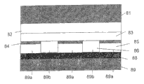
With reference to figure 5a to 5c, such possibility is described now, promptly the light variable element by the surface region of the thin-film component gauge of a part in the one or more replacement layer that is provided with a diffraction structure of coating.
Fig. 5 a illustrates 51, eight layers of a carrier 52 to 59 and a plurality of surface region 59a and 59b.Layer 52 is a protective paint layer and/or separating layer.Layer 53 is a duplicating layer.Layer 54 is an absorbed layer.Layer 56 and 57 is for replacing layer.Layer 58 is a metal level or a high refractive index layer.Layer 59 is a glue-line.
Layer is 52,53,54,55,58 and 59 as Fig. 3 and 4 described embodiment configurations, and as being coated on the carrier 51 as described in this place.
Also can on the surface of layer 53, be coated with diffraction structure, to replace impression by laser.
Follow coating layer 57 in surface region 59b, the latter is preferably a metal level.
Herein, this metallization can obtain by evaporation before or after the thin-film component at constructing part under the situation that adopt diaphragm.
Such possibility is further arranged, promptly on layer 53, obtain the metallization of gross area, and promptly remove metallization in the district at the thin-film component of part at surface region 59a by a kind of in the said method (positive acid etching, negative acid etching, ablation).This thin-film component that is in constructing part of this step carries out before.
Moulding process also can at first carry out after coating layer 57.
Fig. 5 b illustrates a carrier 61, eight layers 62 to 69 and a plurality of surface region 69a and 69b.Layer 62 is a protective paint layer and/or separating layer.Layer 63 is a duplicating layer.Layer 64 is an absorbed layer.Layer 66 and 67 is for replacing layer.Layer 58 is metal level or high refractive index layer.Layer 59 is a glue-line.
Layer is 62,63,64,65,68 and 69 as Fig. 3 and 4 described embodiment configurations, and as being coated on the carrier 61 as described in this place.
With opposite at the embodiment shown in Fig. 5 a, layer 68 only partly constitutes.This can be by reaching as the top said coating of carrying out the part of layer 68.Such possibility is further arranged, promptly when the evaporation of layer 68, carry out the evaporation of layer 67 abreast, and follow partly coating layer 66.But this layer 66 also can be the part (also can referring to the explanation to Fig. 3) of glue-line 69.
Fig. 5 c illustrates a carrier 71, eight layers 72 to 79 and a plurality of surface region 79a and 79b.Layer 72 is a protective paint layer and/or separating layer.Layer 73 is a duplicating layer.Layer 74 is an absorbed layer.Layer 76 and 77 is for replacing layer.Layer 78 is a metal level or high refractive index layer.Layer 79 is a glue-line.
Layer is 72,73,74,75,78 and 79 as Fig. 3 and 4 described embodiment configurations, and as being coated on the carrier 71 as described in this place.
Layer 73 duplicates lacquer by one or is made up of the plastics of a thermoformable.Layer 73 is as at the diffraction structure that is provided with described in the explanation of Fig. 5 a, and is provided with layer 77 in surface region 79a.
With opposite at the embodiment shown in Fig. 5 a and the 5b, layer 77 and 76 both are metal levels.Therefore, metal level 77 will be for example as being coated with by Fig. 5 a is described, and be provided with diffraction structure.By suitable selection to the material that is used for spacing layer 75, can accomplish, make the spacing layer in surface region 79b, metallicity be arranged.Follow gross area ground coating metal layer 79.
Naturally also may be as illustrated in the description that Fig. 5 a is done, coating just has the bigger bed thickness shown in Fig. 5 c as the layer 77 and 76 of single metal level.
Referring to Fig. 6 a and 6b, such possibility is described now, promptly in the surface region by the thin-film component gauge of a part of light variable element, one or more transparent replacement layers is set.
Fig. 6 a illustrates a carrier 81, seven layers 82 to 89 and a plurality of surface region 89a and 89b.Layer 82 is a protective paint layer and/or separating layer.Layer 83 is a duplicating layer.Also can abandon duplicating layer herein.Layer 84 is an absorbed layer.Layer 86 is a replacement layer.Layer 88 is a metal level.Layer 89 is a glue-line.
Layer is 82,83,84,85,88 and 89 as Fig. 3 and 4 described embodiment configurations, and as described in this place, is coated on the carrier 81.
Replace layer 86 to form by a transmission material.This material also can be the material identical materials used with spacing layer 85.Thus, can abandon the part coating of layer 85 and 86 as described in the explanation of Fig. 5 a.
Fig. 6 b illustrates a carrier 91, seven layers 92,93,94,95,96,98 and 99, diffraction structure 97 and a plurality of surface region 99a to 99d.Layer 92 is a protective paint layer and/or separating layer.Layer 93 is a duplicating layer.Layer 94 is an absorbed layer.Layer 96 is a replacement layer.Layer 98 is a metal level.Layer 99 is a glue-line.
Layer is 92,93,94,95,98 and 99 as Fig. 3 and 4 described embodiment configurations, and as described in this place, is coated on the carrier 91.The configuration that replaces layer 96 to be implemented as Fig. 6 a.
Before coating layer 94 and/or layer 96, on the surface of layer 93, be coated with diffraction structure 97 by one of a coining tool or aforesaid other method.As what find out from Fig. 6 b, diffraction structure 97 can be coated with in the surface region that is covered by the thin-film component of part herein, also can be coated with in this surface region that is not covered by the thin-film component of part.
In some possibility shown in Fig. 7 and 8, promptly Bu Fen thin-film component makes up with the diffraction structure of part and the metallization of part.
Fig. 7 illustrates a carrier 101, nine layers 102 to 109 and a plurality of surface region 109a to 109d.Layer 102 is a protective paint layer and/or separating layer.Layer 103 is a duplicating layer.Layer 104 is an absorbed layer.Layer 106,107 and 107a are for replacing layer.Layer 108 is a metal level.Layer 109 is a glue-line.
Layer is 102,103,104,105,108 and 109 as Fig. 3 and 4 described embodiment configurations, and as described in this place, is coated on the carrier 101.
Replacing layer 107 is a metal level, and it is as the configuration described in the embodiment shown in Fig. 5 a and the 5b, and as described in this place, is coated on the carrier 101.
Replacing layer 107 is a metal level, and it can be as building described in the embodiment shown in Fig. 5 a and the 5b.Replace layer 106 and 107a to form by a transmission material.They can be as building described in the embodiment shown in Fig. 6 a and the 6b.
As what can in Fig. 7, see, in surface region 109b, 109d and 109e, on layer 103, further be coated with diffraction structure.
Fig. 8 illustrates 111, eight layers of a carrier 112 to 119 and a plurality of surface region 119a and 119b.Layer 112 is a protective paint layer and/or separating layer.Layer 113 is a duplicating layer.Layer 114 is an absorbed layer.Layer 117 is a spacing layer.Layer 116 and 115 is for replacing layer.Layer 118 is a metal level.Layer 119 is a glue-line.
Layer is 112,113,114,117,118 and 119 as Fig. 3 and 4 described embodiment configurations, and as described in this place, is coated on the carrier 111.
Replacing layer 115 is metal level, and it can be as building described in the embodiment shown in Fig. 5 a and the 5b.Replace layer 116 to form (also can referring to description) to the embodiment of Fig. 3 by a resistance to acid attack thing.
As what can in Fig. 8, see, in surface region 119c and 119d, on layer 113, further be coated with diffraction structure 115a and 115c.
Can be by above-mentioned possible method with the positional precision that reaches 0.2mm by the adaptive independent element of any locational combination results, as the thin-film component of part, the structuring (for example diffraction structure) of part, the metallization of part and the transparent window of part, with as being connected to each other or continuous picture pattern.
Claims (27)
1. light variable element, wherein, this light variable element has one by interfering thin layer series and other layer that produces the change color relevant with the visual angle, wherein, this thin layer series constitutes the thin-film component of part, this thin-film component is subregion ground and press the surface region that pattern form ground covers described other layer only, and described thin layer series has an absorbed layer and transparent λ/4 or λ/2 spacing layers, and perhaps described thin layer series has a plurality of layers with different refractivity.
2. smooth variable element as claimed in claim 1 is characterized by, and described absorbed layer has 30% to 65% transmission.
3. as the light variable element of claim 1 or 2, it is characterized by, described thin layer series has described absorbed layer, described transparent λ/4 spacing layers and reflecting layer, and perhaps described thin layer series has described absorbed layer, described transparent λ/2 spacing layers and transmission layer.
4. smooth variable element as claimed in claim 1 is characterized by, and the thin-film component of part has a reflecting layer.
5. smooth variable element as claimed in claim 1 is characterized by, and the thin-film component of part has a diffraction structure that is used to produce diffraction effect.
6. as the light variable element of claim 1 or 5, it is characterized by, some the reflecting layer of thin-film component of part, this reflecting layer only partly cover the surface region of the thin-film component of described part.
7. smooth variable element as claimed in claim 6 is characterized by, and some the diffraction structure that is used to produce diffraction effect of thin-film component of part, this diffraction structure only partly cover the surface region of the thin-film component of described part.
8. smooth variable element as claimed in claim 1 is characterized by, and the surface region by the thin-film component gauge of part has described absorbed layer, but does not have described spacing layer.
9. smooth variable element as claimed in claim 1 is characterized by, and the surface region by the thin-film component gauge of part has described spacing layer, but does not have described absorbed layer.
10. smooth variable element as claimed in claim 1 is characterized by, and the surface region by the thin-film component gauge of part has one or more replacement layers, and this replaces layer to replace the thin layer series of the thin-film component of described part in this surface region.
11. the light variable element as claim 10 is characterized by, and is surrounded or surround the thin-film component of part by the thin-film component of described part by the surface region of the thin-film component gauge of described part.
12. the light variable element as claim 10 is characterized by, described one or more replacement layer has a total bed thickness of bed thickness that roughly is equivalent to the thin-film component of described part.
13. the light variable element as claim 10 is characterized by, described one or more replacement layer has a diffraction structure that is used to produce diffraction effect.
14. the light variable element as claim 10 or 13 is characterized by, described one or more replacement layer is made of a reflecting layer and a supporting course.
15. the light variable element as claim 10 or 13 is characterized by, described one or more replacement layer is made of a single reflecting layer.
16. the light variable element as claim 10 or 13 is characterized by, described one or more replacement layer is made of one or more transparent layers.
17. the light variable element as claim 10 or 13 is characterized by, described one or more replacement layer has the reflecting layer of a part, and this reflecting layer only partly covers the surface region of described one or more replacement layer.
18. the light variable element as claim 10 is characterized by, described one or more replacement layer has the diffraction structure that is used to produce diffraction effect of a part, and this diffraction structure only partly covers the surface region of described one or more replacement layer.
19. smooth variable element as claimed in claim 1 is characterized by, described other layer is the hyaline layer of a gross area.
20. the light variable element as claim 19 is characterized by, described hyaline layer is a protective paint layer.
21. smooth variable element as claimed in claim 1 is characterized by, described other layer is the reflecting layer of a gross area.
22. the light variable element as claim 21 is characterized by, the reflecting layer of described gross area is a metal level.
23. smooth variable element as claimed in claim 1 is characterized by, described other layer is the glue-line of a gross area.
24. have the Protection Product of the light variable element of one of claim as described above.
25. the Protection Product as claim 24 is characterized by, described Protection Product is bank note or credit card.
26. have paper tinsel as the light variable element of one of claim 1 to 23.
27. the paper tinsel as claim 26 is characterized by, described paper tinsel is embossing film or lamination paper tinsel.
Applications Claiming Priority (2)
| Application Number | Priority Date | Filing Date | Title |
|---|---|---|---|
| EP02010745 | 2002-05-14 | ||
| EP02010745.4 | 2002-05-14 |
Publications (2)
| Publication Number | Publication Date |
|---|---|
| CN1652946A CN1652946A (en) | 2005-08-10 |
| CN100534806C true CN100534806C (en) | 2009-09-02 |
Family
ID=29414683
Family Applications (1)
| Application Number | Title | Priority Date | Filing Date |
|---|---|---|---|
| CNB038107724A Expired - Fee Related CN100534806C (en) | 2002-05-14 | 2003-04-17 | Optically variable element comprising a sequence of thin-film layers |
Country Status (12)
| Country | Link |
|---|---|
| US (1) | US6982832B2 (en) |
| EP (1) | EP1503907B1 (en) |
| JP (1) | JP4660187B2 (en) |
| KR (1) | KR100587984B1 (en) |
| CN (1) | CN100534806C (en) |
| AT (1) | ATE352430T1 (en) |
| AU (1) | AU2003222822A1 (en) |
| DE (1) | DE50306381D1 (en) |
| ES (1) | ES2279944T3 (en) |
| PL (1) | PL208667B1 (en) |
| RU (1) | RU2309050C2 (en) |
| WO (1) | WO2003095228A1 (en) |
Families Citing this family (37)
| Publication number | Priority date | Publication date | Assignee | Title |
|---|---|---|---|---|
| KR101110767B1 (en) | 2003-07-14 | 2012-02-24 | 플렉스 프로덕츠, 인코포레이티드 | Security products with overt and/or covert patterned layers and the method for producing the same |
| DE102004003984A1 (en) † | 2004-01-26 | 2005-08-11 | Giesecke & Devrient Gmbh | Lattice image with one or more grid fields |
| AT501989B1 (en) | 2004-03-26 | 2010-04-15 | Hueck Folien Gmbh | SAFETY FEATURES WITH CHARACTERISTICS VISIBLE UNDER A SPECIFIC OVERVIEW |
| DE102004016596B4 (en) * | 2004-04-03 | 2006-07-27 | Ovd Kinegram Ag | Security element in the form of a multilayer film body and method for producing a security element |
| EP1602508A1 (en) * | 2004-06-04 | 2005-12-07 | Axalto SA | Process and apparatus for manufacturing a "hologram-like" device fixed on an object |
| DE102004042136B4 (en) * | 2004-08-30 | 2006-11-09 | Ovd Kinegram Ag | Metallized security element |
| EP1652688A1 (en) * | 2004-10-29 | 2006-05-03 | Arjowiggins Security | Security device |
| DE102005006074B4 (en) * | 2005-02-10 | 2009-12-10 | Leonhard Kurz Gmbh & Co. Kg | Decorated injection molded article and method of making the decorated injection molded article |
| DE102005049891A1 (en) * | 2005-10-17 | 2007-04-19 | Leonhard Kurz Gmbh & Co. Kg | Metallized multilayer body |
| DE102006037431A1 (en) * | 2006-08-09 | 2008-04-17 | Ovd Kinegram Ag | Production of multi-layer bodies useful in element for security- and value document such as banknotes and credit cards, by forming a relief structure in an area of replication layer and applying a layer on carrier and/or replication layer |
| TWI447033B (en) * | 2006-08-09 | 2014-08-01 | Ovd Kinegram Ag | Verfahren zur herstellung eines mehrschichtkoerpers sowie mehrschichtkoerper |
| JP2008134586A (en) * | 2006-10-23 | 2008-06-12 | Toppan Printing Co Ltd | Display element and display body |
| JP2008275740A (en) * | 2007-04-26 | 2008-11-13 | Toppan Printing Co Ltd | Display body and laminate |
| DE102007034716A1 (en) † | 2007-07-23 | 2009-01-29 | Giesecke & Devrient Gmbh | security element |
| FR2921584A1 (en) | 2007-09-28 | 2009-04-03 | Oberthur Card Syst Sa | SECURE DOCUMENTS, METHODS AND DEVICES FOR AUTHENTICATING SUCH DOCUMENTS AND METHOD FOR MANUFACTURING THE SAME. |
| DE102007061828A1 (en) | 2007-12-20 | 2009-06-25 | Giesecke & Devrient Gmbh | Security element and method for its production |
| DE102007061827A1 (en) * | 2007-12-20 | 2009-06-25 | Giesecke & Devrient Gmbh | Security element and method for its production |
| DE102008009296A1 (en) * | 2008-02-15 | 2009-08-20 | Giesecke & Devrient Gmbh | Security element and method for its production |
| DE102008013073B4 (en) | 2008-03-06 | 2011-02-03 | Leonhard Kurz Stiftung & Co. Kg | Process for producing a film element and film element |
| DE102008013167A1 (en) | 2008-03-07 | 2009-09-10 | Giesecke & Devrient Gmbh | Security element and method for its production |
| DE102008017652A1 (en) | 2008-04-04 | 2009-10-08 | Leonhard Kurz Stiftung & Co. Kg | Security element and method for producing a security element |
| DE102008024147B4 (en) * | 2008-05-19 | 2020-12-03 | Ovd Kinegram Ag | Optical security element |
| DE102008028187A1 (en) * | 2008-06-12 | 2009-12-17 | Giesecke & Devrient Gmbh | Security element with optically variable element. |
| DE102008027952A1 (en) | 2008-06-12 | 2009-12-17 | Giesecke & Devrient Gmbh | Security element with screened layer of raster elements |
| DE102008030409A1 (en) † | 2008-06-27 | 2009-12-31 | Giesecke & Devrient Gmbh | Safety element with recess and method for producing the same |
| DE102008036670B3 (en) * | 2008-08-06 | 2009-11-26 | Leonhard Kurz Stiftung & Co. Kg | Film, process for its preparation, and use |
| DE102009008853A1 (en) | 2009-02-13 | 2010-08-19 | Giesecke & Devrient Gmbh | Through security element |
| BR112013003855A2 (en) * | 2010-08-23 | 2016-07-12 | Securency Int Pty Ltd | optically variable multichannel device |
| FR2993204B1 (en) * | 2012-07-16 | 2018-02-02 | Oberthur Fiduciaire Sas | SAFETY STRUCTURE. |
| GB201400910D0 (en) * | 2014-01-20 | 2014-03-05 | Rue De Int Ltd | Security elements and methods of their manufacture |
| US9857544B2 (en) * | 2015-10-09 | 2018-01-02 | Te Connectivity Nederland B.V. | Carrier having ablation-susceptible and ablation-insusceptible materials |
| EP3594016A4 (en) | 2017-03-06 | 2020-03-18 | LG Chem, Ltd. | Decorative member and method for manufacturing decorative member |
| KR101966851B1 (en) * | 2017-03-06 | 2019-04-08 | 주식회사 엘지화학 | Decoration element and preparing method thereof |
| DE102018003030A1 (en) * | 2018-04-13 | 2019-10-17 | Giesecke+Devrient Currency Technology Gmbh | Security element, method for producing the same and equipped with the security element disk |
| EP3650240A1 (en) * | 2018-11-09 | 2020-05-13 | Gemalto AG | Multiple color image |
| EP3726506B1 (en) | 2019-04-19 | 2022-10-26 | Securikett Ulrich & Horn GmbH | Sealing film |
| CN111098617A (en) * | 2020-01-09 | 2020-05-05 | 武汉红金龙印务股份有限公司 | Latent image embossing anti-counterfeiting structure and preparation process thereof |
Citations (3)
| Publication number | Priority date | Publication date | Assignee | Title |
|---|---|---|---|---|
| DE2545799A1 (en) * | 1975-10-13 | 1977-04-21 | Unitec Gmbh & Co Kg | Credit card with data invisible to naked eye - uses multilayered card with holographic data only visible when placed in optical reader |
| US4184700A (en) * | 1975-11-17 | 1980-01-22 | Lgz Landis & Gyr Zug Ag | Documents embossed with optical markings representing genuineness information |
| US5801857A (en) * | 1989-09-28 | 1998-09-01 | Gao Gesellschaft Fur Automation Und Organisation Mbh | Data carrier having an optically variable element and methods for producing it |
Family Cites Families (4)
| Publication number | Priority date | Publication date | Assignee | Title |
|---|---|---|---|---|
| JPH08118857A (en) * | 1994-10-28 | 1996-05-14 | Dainippon Printing Co Ltd | Preventing method for forgery and alteration of information recording medium, information recording medium designed so as to prevent forgery and alteration, and transfer sheet |
| JPH09254520A (en) * | 1996-03-26 | 1997-09-30 | Dainippon Printing Co Ltd | Color changing card |
| US6761959B1 (en) * | 1999-07-08 | 2004-07-13 | Flex Products, Inc. | Diffractive surfaces with color shifting backgrounds |
| GB0015873D0 (en) * | 2000-06-28 | 2000-08-23 | Rue De Int Ltd | Optically variable security device |
-
2003
- 2003-04-17 US US10/513,521 patent/US6982832B2/en not_active Expired - Lifetime
- 2003-04-17 PL PL373142A patent/PL208667B1/en unknown
- 2003-04-17 RU RU2004136320/12A patent/RU2309050C2/en not_active IP Right Cessation
- 2003-04-17 EP EP03718769A patent/EP1503907B1/en not_active Expired - Lifetime
- 2003-04-17 AU AU2003222822A patent/AU2003222822A1/en not_active Abandoned
- 2003-04-17 KR KR1020047018251A patent/KR100587984B1/en not_active IP Right Cessation
- 2003-04-17 WO PCT/EP2003/004023 patent/WO2003095228A1/en active IP Right Grant
- 2003-04-17 JP JP2004503282A patent/JP4660187B2/en not_active Expired - Fee Related
- 2003-04-17 ES ES03718769T patent/ES2279944T3/en not_active Expired - Lifetime
- 2003-04-17 CN CNB038107724A patent/CN100534806C/en not_active Expired - Fee Related
- 2003-04-17 AT AT03718769T patent/ATE352430T1/en active
- 2003-04-17 DE DE50306381T patent/DE50306381D1/en not_active Expired - Lifetime
Patent Citations (3)
| Publication number | Priority date | Publication date | Assignee | Title |
|---|---|---|---|---|
| DE2545799A1 (en) * | 1975-10-13 | 1977-04-21 | Unitec Gmbh & Co Kg | Credit card with data invisible to naked eye - uses multilayered card with holographic data only visible when placed in optical reader |
| US4184700A (en) * | 1975-11-17 | 1980-01-22 | Lgz Landis & Gyr Zug Ag | Documents embossed with optical markings representing genuineness information |
| US5801857A (en) * | 1989-09-28 | 1998-09-01 | Gao Gesellschaft Fur Automation Und Organisation Mbh | Data carrier having an optically variable element and methods for producing it |
Also Published As
| Publication number | Publication date |
|---|---|
| CN1652946A (en) | 2005-08-10 |
| JP4660187B2 (en) | 2011-03-30 |
| WO2003095228A1 (en) | 2003-11-20 |
| KR100587984B1 (en) | 2006-06-08 |
| JP2006504545A (en) | 2006-02-09 |
| AU2003222822A1 (en) | 2003-11-11 |
| ATE352430T1 (en) | 2007-02-15 |
| RU2309050C2 (en) | 2007-10-27 |
| EP1503907A1 (en) | 2005-02-09 |
| DE50306381D1 (en) | 2007-03-15 |
| US6982832B2 (en) | 2006-01-03 |
| PL373142A1 (en) | 2005-08-22 |
| KR20050007537A (en) | 2005-01-19 |
| EP1503907B1 (en) | 2007-01-24 |
| ES2279944T3 (en) | 2007-09-01 |
| US20050141094A1 (en) | 2005-06-30 |
| PL208667B1 (en) | 2011-05-31 |
| RU2004136320A (en) | 2005-05-27 |
Similar Documents
| Publication | Publication Date | Title |
|---|---|---|
| CN100534806C (en) | Optically variable element comprising a sequence of thin-film layers | |
| CN100429083C (en) | Optically variable element comprising a partially transparent element | |
| JP4308020B2 (en) | Security documents and security elements for security documents | |
| JP4509571B2 (en) | Security elements and security documents with security elements | |
| JP4256343B2 (en) | Optical variable element having spacer layers having various layer thicknesses | |
| CN101790464B (en) | Safety element | |
| EP2951029B1 (en) | Security devices and methods of manufacture thereof | |
| RU2313456C2 (en) | Protective element with color kipp effect and magnetic properties, object with such a protective element, and method for manufacturing such protective element and such object | |
| CN1589205A (en) | Security element for security papers and valuable documents | |
| EP3445592B1 (en) | Security devices and methods of manufacture thereof | |
| CN1854944B (en) | Patterned structures with optically variable effects | |
| CA2703616C (en) | Security document and method for the production thereof |
Legal Events
| Date | Code | Title | Description |
|---|---|---|---|
| C06 | Publication | ||
| PB01 | Publication | ||
| C10 | Entry into substantive examination | ||
| SE01 | Entry into force of request for substantive examination | ||
| C14 | Grant of patent or utility model | ||
| GR01 | Patent grant | ||
| CF01 | Termination of patent right due to non-payment of annual fee | ||
| CF01 | Termination of patent right due to non-payment of annual fee |
Granted publication date: 20090902 Termination date: 20190417 |